Blind & Buried Via PCB: Complete Manufacturing, Design, Materials & Cost Guide
Blind and buried via PCBs enable high-density interconnections without using through-holes across the entire board thickness. They are commonly used in multilayer and HDI designs where routing space, component density, and layer connectivity are critical. Shenzhen Hongda Circuit Technology Co., Ltd. provides PCB fabrication and PCBA assembly for custom multilayer designs. Our engineering team reviews stackups, via structures, and manufacturing files before production. Send your PCB files to sales@pcbkr.com for a manufacturing review and quotation.
1. What Is a Blind & Buried Via PCB?
A blind and buried via PCB is a multilayer printed circuit board that uses non-through-hole vias to connect selected layers within the board.
Unlike a conventional through-hole via, which passes through the full PCB thickness, a blind via connects an outer layer to one or more inner layers, while a buried via connects internal layers without reaching either external surface.
These via structures are used when a PCB requires more routing space, higher component density, or more flexible layer-to-layer connections.
What Is a Blind Via?
A blind via connects an external copper layer to one or more internal copper layers but does not extend through the entire board.
For example, a blind via may connect Layer 1 to Layer 2 or Layer 1 to Layer 3, depending on the board’s stackup and manufacturing process.
Blind vias can help free routing space on inner layers and support dense component layouts, particularly around fine-pitch BGA packages.
What Is a Buried Via?
A buried via connects two or more internal copper layers and remains enclosed within the finished PCB.
Because it does not reach the outer surfaces, a buried via can provide internal layer connectivity without occupying an external routing location.
Buried vias are generally formed within an inner-layer subassembly before additional layers are laminated around it. The exact manufacturing sequence depends on the required layer connection and stackup.
Why Are Blind and Buried Vias Used?
Designers may consider blind and buried vias when:
- Through-hole vias consume too much routing space.
- Dense BGA packages require additional fan-out options.
- The board needs connections between selected layers.
- Component placement limits the available routing area.
- A multilayer HDI design requires more flexible interconnection structures.
However, blind and buried vias are not automatically the best solution for every multilayer PCB. Their use introduces additional manufacturing steps, design constraints, and cost considerations. The complete stackup should be reviewed before the via structure is finalized.
2. Blind Via vs. Buried Via vs. Through-Hole Via
The main difference between these via types is which copper layers they connect and whether they extend to the external surfaces.
| Via Type | Layer Connection | Extends Through Full Board? | Typical Design Purpose |
|---|---|---|---|
| Through-hole via | Connects layers along the full board thickness | Yes | General multilayer interconnection |
| Blind via | Connects an outer layer to selected inner layers | No | Outer-layer routing density and component fan-out |
| Buried via | Connects selected internal layers | No | Internal layer interconnection |
| Microvia | Typically connects adjacent or closely spaced layers in an HDI build-up structure | No | Fine-pitch component fan-out and high-density routing |
Blind Via vs. Buried Via
A blind via starts at an external surface and terminates at an internal layer. A buried via is contained entirely within the internal layers.
The choice depends on where the electrical connection is required, how the stackup is constructed, and which routing layers need to remain available.
Blind Via vs. Through-Hole Via
A through-hole via is usually simpler to incorporate into a conventional multilayer design, but it occupies space through the full board thickness.
A blind via can preserve routing space on layers beyond its termination point. This can be useful in dense designs, although the additional manufacturing complexity may increase cost.
Buried Via vs. Through-Hole Via
A buried via provides internal connectivity without using an external surface location. It may be useful when internal routing density is high and external routing resources are limited.
The trade-off is that buried vias require a manufacturing sequence capable of forming and enclosing the internal connection.
For a more detailed comparison of connectivity, design trade-offs, and manufacturing considerations, see our guide to blind via vs. buried via PCB comparison.
3. Common Blind & Buried Via PCB Structures
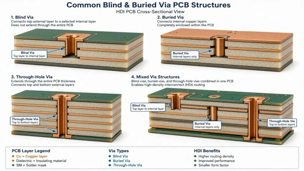
Common blind and buried via PCB structures showing blind vias, buried vias and through-hole vias
Blind and buried via structures are defined by their starting and ending layers, not simply by the total number of PCB layers.
A design should specify each via’s layer span clearly so that the PCB manufacturer can evaluate the required drilling, plating, and lamination sequence.
Blind Via Layer Spans
Common examples include:
- L1–L2: connects the top surface to the first internal layer.
- L1–L3: connects the top surface to a deeper internal layer.
- L10–L12: connects selected internal layers to the bottom surface in a corresponding stackup.
These are illustrative layer-span descriptions. Whether a particular structure is manufacturable depends on the board construction, dielectric thickness, drilling method, and process capability.
Buried Via Layer Spans
Buried vias connect internal layers, such as:
- L2–L3.
- L2–L4.
- L3–L6.
The actual connection must be compatible with the inner-layer core structure and lamination sequence.
Mixed Via Structures in HDI PCBs
Some HDI designs combine through-hole vias, blind vias, buried vias, and microvias.
For example, a board may use through-hole vias for general layer connections, blind vias for BGA fan-out, and buried vias for selected internal routing transitions.
This approach can provide greater routing flexibility, but the combined via structure must be checked for:
- Layer connectivity.
- Drill access.
- Lamination sequence.
- Copper plating requirements.
- Via-to-via and via-to-pad clearances.
- Manufacturability and inspection requirements.
The final structure should be based on the electrical and mechanical requirements of the product rather than selecting the highest possible via complexity.
4. Blind & Buried Via PCB Manufacturing Process
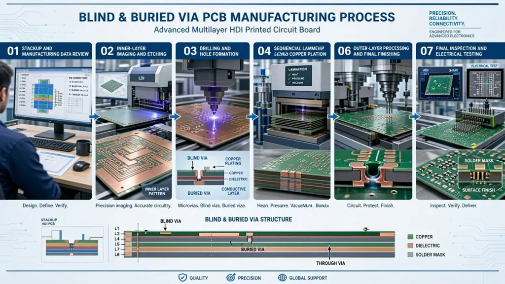
Blind and buried via PCB manufacturing process showing laser drilling, copper plating and sequential lamination
Blind and buried via PCB manufacturing requires careful coordination between inner-layer fabrication, drilling, plating, lamination, and final inspection.
The exact process sequence depends on the selected layer spans and board construction. Not every blind or buried via design uses the same drilling or lamination method.
Step 1: Stackup and Manufacturing Data Review
Before production, the manufacturer reviews:
- Total layer count.
- Core and build-up structure.
- Blind and buried via layer spans.
- Dielectric thicknesses.
- Copper weights.
- Drill data.
- Via filling and capping requirements.
- Registration and clearance requirements.
The objective is to confirm that the proposed structure can be translated into a practical manufacturing sequence.
Step 2: Inner-Layer Imaging and Etching
Copper-clad cores are processed according to the approved inner-layer data.
Imaging transfers the circuit pattern onto the copper surface, followed by the relevant etching and inspection operations.
PCBKR uses SCREEN Ledia LDI equipment with an 8 µm target imaging capability and a stated ±10 µm imaging tolerance. This figure describes the LDI imaging capability; it should not be interpreted as a finished-board layer-registration guarantee.
Step 3: Drilling and Hole Formation
The drilling method depends on the via structure, required geometry, material, and layer span.
Mechanical drilling may be used for applicable buried or through-hole structures. Laser drilling is commonly used for suitable HDI blind microvia structures.
PCBKR has confirmed Mitsubishi UV/CO₂ laser capability of 75 µm ±5 µm and picosecond laser capability of 50 µm. These are process capability references, not universal finished-via acceptance limits. The applicable structure and achievable result must be confirmed during engineering review.
Step 4: Desmear and Copper Plating
After drilling, the hole walls and exposed internal copper interfaces must be prepared for reliable electrical connection.
Depending on the material and process route, desmear and hole-wall preparation are followed by copper deposition and plating.
Process controls must account for:
- Hole-wall cleanliness.
- Copper coverage.
- Connection to the target copper layer.
- Plating uniformity.
- Potential voids or other defects.
The required copper thickness and acceptance criteria should be defined by the customer specification and the applicable PCB construction requirements.
Step 5: Sequential Lamination
Sequential lamination is used when the board requires multiple stages of inner-layer and build-up construction.
An internal subassembly may be fabricated first, followed by additional dielectric and copper layers. Further drilling, plating, and lamination operations may then be required to complete the design.
The number of lamination cycles depends on the selected structure. A board with blind and buried vias does not automatically require a fixed number of press cycles.
PCBKR uses LAUFFER lamination equipment with confirmed pressure settings of 80, 150, and 200 psi and vacuum below 50 mbar. These are equipment process parameters; the actual production recipe depends on the material system, stackup, and engineering process window.
Step 6: Outer-Layer Processing and Final Finishing
After the required build-up and lamination operations, the remaining outer-layer imaging, etching, solder mask, surface finish, and other specified operations are completed.
The selected surface finish and any special via filling, plugging, or copper capping requirements should be included in the manufacturing documentation.
Step 7: Final Inspection and Electrical Testing
The completed board is inspected according to its drawing, customer requirements, and applicable acceptance criteria.
Available PCBKR inspection and test equipment includes:
- 3D AOI.
- X-ray inspection.
- Four-wire Kelvin flying probe testing.
The inspection plan should be selected according to the via construction and risk. A particular test method should not be assumed to be mandatory or included in every order unless it is specified and agreed.
5. Material Selection for Blind & Buried Via PCBs
Material selection affects lamination compatibility, dimensional stability, electrical performance, and the reliability of multilayer interconnections.
The best material is not necessarily the material with the highest Tg or lowest dielectric constant. It must be suitable for the board’s electrical requirements and the selected manufacturing sequence.
Glass-Reinforced Epoxy Materials
FR-4-based materials are used in many multilayer PCB designs. Different grades have different thermal, mechanical, and electrical properties.
For blind and buried via applications, the material should be evaluated for:
- Glass transition temperature (Tg).
- Decomposition temperature (Td).
- Z-axis coefficient of thermal expansion.
- Resin content and glass construction.
- Lamination compatibility.
- Dielectric constant and dissipation factor, where signal performance requires them.
High-Tg and Low-CTE Materials
High-Tg or lower-CTE material systems may be considered when the board has demanding thermal exposure, multiple lamination stages, or reliability requirements.
Material selection should consider the complete stackup rather than treating one material property as a standalone guarantee of reliability.
High-Speed and High-Frequency Materials
For high-speed or high-frequency designs, dielectric constant, dissipation factor, copper profile, and signal-path geometry may influence material selection.
The chosen material must also be compatible with the required multilayer construction and lamination process.
Material Compatibility with Sequential Lamination
In a sequentially laminated board, the material system must be evaluated for compatibility across the relevant press cycles.
Important considerations include:
- Resin flow and dielectric thickness control.
- Curing behavior.
- Dimensional stability.
- Copper adhesion.
- Thermal expansion.
- Compatibility between core and build-up materials.
For a more detailed discussion of material properties and selection criteria, refer to our guide to PCB materials for blind via HDI designs.
6. Stackup Design and Layer Transition Planning
A blind and buried via design should begin with a complete stackup, not with an isolated drill-size decision.
The stackup determines which layers can be connected, where the via starts and terminates, and how the board can be manufactured.
Define the Required Layer Connections
The design team should identify:
- Which signal layers require direct connections.
- Which power and ground layers require transitions.
- Where blind vias are needed for external-layer access.
- Where buried vias are needed for internal connections.
- Whether conventional through-hole vias can satisfy some connections.
This prevents unnecessary use of complex via structures.
Plan the Core and Build-Up Structure
A multilayer HDI board may contain one or more core sections and additional build-up layers.
The manufacturer needs to understand how the proposed blind and buried via spans relate to these sections.
A via that appears straightforward in a schematic or routing layout may require a different manufacturing sequence once the complete stackup is considered.
Coordinate Layer Transitions with Routing
Via locations and layer transitions affect routing availability.
Designers should review:
- Capture pad dimensions.
- Clearance to adjacent copper.
- Trace escape around BGA pads.
- Via-to-via spacing.
- Power and ground connections.
- Remaining routing channels.
Review the Lamination Sequence
The stackup must be compatible with the intended lamination sequence.
The design team and manufacturer should agree on the core construction, build-up stages, drilling sequence, and required layer connections before the design is released for production.
For more detailed design considerations, see our guide to buried via HDI PCB stackup design.
7. DFM Requirements for Blind & Buried Via PCBs
Design for Manufacturability (DFM) is particularly important for blind and buried via boards because a small change in layer span or via geometry can affect the manufacturing sequence.
The following items should be reviewed before the design is finalized.
Via Diameter and Aspect Ratio
Via diameter and aspect ratio influence drilling, desmear, plating, and the overall manufacturability of the structure.
There is no single aspect-ratio limit that applies to every blind or buried via. The acceptable range depends on the via type, drilling method, dielectric thickness, plating process, and supplier capability.
Designers should provide the actual via geometry and layer span rather than relying on generic design-rule values.
Capture Pads and Annular Rings
The target pad must provide sufficient copper area for the intended connection.
The design review should consider:
- Target pad dimensions.
- Drill diameter.
- Registration allowance.
- Annular ring requirements.
- Adjacent copper clearance.
- The effect of the via on surrounding routing.
The required annular ring should be established using the design specification and the selected manufacturer’s verified process capability.
Via Filling and Copper Capping
Some designs require resin-filled, conductive-filled, or copper-filled vias. Others require a capped surface for component mounting or routing.
These are different manufacturing requirements and should not be treated as interchangeable.
The fabrication drawing should clearly identify:
- Which vias require filling.
- The required filling material.
- Whether copper capping is required.
- Whether the via is located in a component pad.
- The applicable surface and planarity requirements.
The manufacturer should confirm the process route and acceptance criteria before quotation.
Layer Registration and Clearance
Blind and buried via structures require accurate alignment between drilled holes and target copper features.
The design should provide appropriate registration allowances and clearances based on the selected manufacturing process.
Do not confuse LDI imaging tolerance with finished-board layer-to-layer registration. These are different process characteristics and must be evaluated separately.
Avoid Unnecessary Via Complexity
Not every electrical connection needs a blind or buried via.
Where routing and electrical requirements permit, a through-hole via or a simpler layer transition may reduce manufacturing complexity.
A good DFM review should identify where the design can be simplified without compromising the required electrical and mechanical performance.
8. What Files Are Required for a Blind & Buried Via PCB Quote?
A complete RFQ package helps the manufacturer evaluate the design, identify missing information, and provide a more reliable quotation.
For blind and buried via PCBs, the layer connection information is particularly important.
1. Gerber or Other Approved Fabrication Data
Provide the fabrication data for each copper layer, along with solder mask, silkscreen, and other required manufacturing layers.
The data format should be agreed with the manufacturer.
2. NC Drill Files
Provide drill data that identifies the required hole structures.
Where the design uses different blind, buried, and through-hole connections, the drill information must make the relevant structures and layer spans clear.
Do not assume that one undifferentiated drill file is sufficient for every HDI construction.
3. PCB Stackup and Layer Map
The stackup should identify:
- Total layer count.
- Copper thickness by layer.
- Core and dielectric materials.
- Dielectric thicknesses.
- Finished board thickness.
- Blind and buried via layer spans.
- Build-up structure, where applicable.
4. Fabrication Drawing
The drawing should specify relevant manufacturing requirements, such as:
- Board dimensions and tolerances.
- Finished hole requirements.
- Surface finish.
- Solder mask and legend.
- Controlled impedance, if applicable.
- Via filling and capping.
- Special inspection or acceptance requirements.
5. Material and Performance Requirements
Specify the required material grade or electrical and thermal properties.
For high-speed designs, include the relevant impedance requirements and stackup information.
For products with special reliability requirements, identify the applicable qualification and acceptance criteria.
6. Quantity and Delivery Requirements
Include prototype quantity, production quantity, target delivery date, and any required packaging or shipping conditions.
If PCBA assembly is also required, provide the BOM, assembly data, and any applicable assembly specifications separately.
A complete package allows the engineering team to evaluate the design before production. If the stackup, layer span, or via requirements are unclear, clarification should be completed before the quotation is treated as final.
9. Quality Control and Reliability Verification
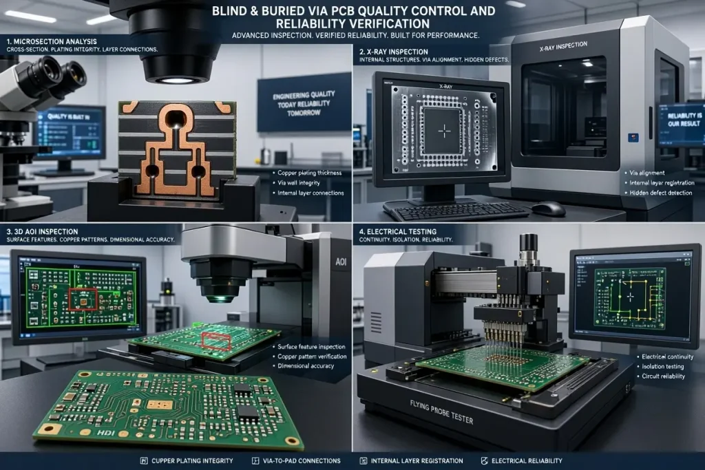
Blind and buried via PCB inspection using microsection analysis, X-ray, 3D AOI, and electrical testing to verify internal connections and manufacturing quality.
Blind and buried via quality depends on the integrity of the drilled connection, copper plating, target-pad connection, and multilayer structure.
Inspection and testing should be selected according to the construction, application, customer specification, and applicable acceptance criteria.
Visual and Automated Optical Inspection
AOI can be used to inspect accessible copper patterns and identify relevant surface defects.
For multilayer boards, the inspection plan must account for which features are visible at each manufacturing stage.
AOI should not be described as a direct substitute for internal via inspection.
X-Ray Inspection
X-ray inspection can help examine selected internal structures and identify certain defects that are not visible from the board surface.
Its suitability depends on the structure, material contrast, equipment capability, and inspection objective.
Microsection Analysis
Microsectioning can provide cross-sectional evidence of internal construction, including:
- Hole-wall copper condition.
- Copper-to-target-pad connection.
- Plating thickness.
- Resin and dielectric structure.
- Certain voids, cracks, or separation defects.
The sample location, frequency, and acceptance criteria should be defined by the applicable quality plan.
Electrical Testing
Electrical testing can verify specified continuity and isolation requirements.
PCBKR has four-wire Kelvin flying probe capability for applicable electrical measurements. The test method and coverage should be agreed based on the board design and test requirements.
Reliability Testing
Depending on the application, customers may specify additional reliability evaluations, such as thermal cycling, thermal stress, or other qualification tests.
These tests should not automatically be assumed to be included in every production order. The required test conditions, sample size, acceptance limits, and reporting format should be agreed before production.
10. Blind & Buried Via PCB Cost and Lead Time Factors
Blind and buried via PCBs generally require more manufacturing planning than conventional multilayer boards. Their actual cost and lead time depend on the design and production requirements.
Layer Count and Stackup Complexity
More layers can increase material usage, process time, and manufacturing complexity.
However, total layer count alone does not determine cost. The layer arrangement and via connection structure are also important.
Sequential Lamination Requirements
Additional lamination stages may increase process time and require more engineering coordination.
The number of required stages depends on the construction and layer spans, not simply on whether the board contains blind or buried vias.
Drilling and Via Geometry
The drilling method, hole geometry, dielectric thickness, and required via treatment affect the manufacturing route.
Specialized via filling or copper capping may also add process steps.
Material Selection
Material cost and processing requirements vary with the selected laminate system.
High-performance materials may require different handling and lamination controls compared with conventional FR-4-based constructions.
Inspection and Testing Requirements
Additional inspection, microsection analysis, electrical testing, or qualification requirements may affect the quotation and delivery schedule.
The RFQ should identify which tests are mandatory and which are optional.
Prototype vs. Production Quantity
Prototype and production orders may have different setup, engineering, and unit-cost structures.
A prototype quotation should not automatically be treated as the final production price. Material availability, process validation, quantity, and agreed specifications can change the commercial terms.
What Should Buyers Provide for an Accurate Quote?
At minimum, provide the PCB fabrication data, complete stackup, via layer spans, board dimensions, material requirements, copper weights, surface finish, quantity, and target delivery date.
For a more detailed breakdown, see our guide to blind via PCB cost factors.
11. How to Optimize Blind & Buried Via PCB Design and Cost
The goal of design optimization is not to remove all blind and buried vias. It is to use them only where they provide a necessary routing or electrical benefit.
Consider Through-Hole Vias Where Appropriate
If a connection can be routed through the full board without creating unacceptable routing or electrical constraints, a through-hole via may be a simpler alternative.
This should be evaluated against component placement, routing density, and signal requirements.
Evaluate Blind Via and Microvia Options
Blind vias and microvias can serve different purposes depending on their geometry, layer span, and construction.
A design that requires fine-pitch BGA fan-out may benefit from a suitable microvia structure, while other layer connections may require a different blind via arrangement.
The terms should not be treated as interchangeable without checking the actual construction.
Consider Back Drilling for Applicable Signal Paths
Back drilling can remove unused portions of through-hole via barrels in certain high-speed designs.
It is not a universal replacement for blind or buried vias. The choice depends on the signal path, stub requirements, layer connectivity, and manufacturing constraints.
Review the Stackup Before Increasing Via Complexity
A revised layer arrangement may sometimes simplify the required via structure.
Before adding another blind or buried via span, review whether the required connections can be achieved through a different stackup or routing allocation.
Request DFM Feedback Before Design Release
Early manufacturer involvement can help identify:
- Unnecessary via transitions.
- Incomplete drill data.
- Conflicting layer-span definitions.
- Insufficient target-pad clearances.
- Incompatible filling and capping requirements.
- Stackup and lamination issues.
This review is particularly valuable before a design is frozen for prototype production.
12. Choosing a Blind & Buried Via PCB Manufacturer
Selecting a manufacturer involves more than checking whether a supplier advertises blind and buried via capability.
The buyer should confirm whether the supplier can evaluate the actual design, define a feasible process route, and manufacture the required construction under agreed acceptance criteria.
Verify Equipment and Process Capabilities
Ask the manufacturer to explain which drilling, imaging, lamination, plating, and inspection processes are available.
PCBKR’s confirmed equipment and process references include:
- SCREEN Ledia LDI: 8 µm target imaging capability with stated ±10 µm imaging tolerance.
- Mitsubishi UV/CO₂ laser: confirmed 75 µm ±5 µm laser process capability.
- Picosecond laser: confirmed 50 µm capability.
- LAUFFER lamination equipment: 80, 150, and 200 psi pressure settings, with vacuum below 50 mbar.
- 3D AOI and X-ray inspection.
- Four-wire Kelvin flying probe testing.
These figures describe confirmed equipment or process references. They should not be interpreted as universal finished-board guarantees. The applicable via structure, material, stackup, and acceptance criteria must be reviewed for each project.
Evaluate Engineering and DFM Support
A qualified supplier should be able to review the stackup, drill files, via spans, and manufacturing notes.
Before placing an order, ask whether the supplier can identify missing data, conflicting requirements, and structures that may need redesign.
Confirm Inspection and Documentation Requirements
Discuss which inspections and tests are available for the specific board construction.
Where required, agree on inspection coverage, microsection locations, electrical test requirements, reports, and acceptance criteria.
Do not rely on broad claims such as 100% internal inspection unless the exact inspection method and scope have been confirmed.
Confirm Prototype and Production Support
Ask whether the manufacturer can support the required prototype quantity and the planned production volume.
The quotation should clarify engineering review, material procurement, tooling or setup requirements, production lead time, and any conditions that may affect delivery.
Clarify PCB Fabrication and PCBA Assembly Scope
Some projects require bare PCB fabrication only, while others require component sourcing and PCBA assembly.
Confirm the delivery scope separately:
- Bare PCB fabrication.
- PCB fabrication with customer-supplied components.
- PCB fabrication with component sourcing.
- SMT and THT assembly.
- Additional testing or programming, if specifically agreed.
These services should be included in the quotation only when they are part of the customer’s project requirements.
Work with Hongda Circuit
Shenzhen Hongda Circuit Technology Co., Ltd. provides custom PCB fabrication and PCBA assembly for prototype, small-batch, and production requirements.
For blind and buried via projects, our engineering review focuses on the proposed stackup, layer connections, drilling requirements, material selection, and manufacturing documentation.
To request a quotation, send the following information to sales@pcbkr.com:
- Gerber or approved fabrication files.
- NC Drill files.
- PCB stackup and layer map.
- Board dimensions and thickness.
- Material and copper requirements.
- Blind and buried via layer spans.
- Quantity and target delivery date.
Our team can review the submitted information and clarify manufacturing requirements before quotation.
13. Frequently Asked Questions
What is the difference between a blind via and a buried via in a PCB?
A blind via connects an external PCB layer to one or more internal layers but does not pass through the entire board. A buried via connects internal layers and remains enclosed within the finished PCB. The main difference is whether the via reaches an external surface.
When should a PCB design use blind vias or buried vias instead of through-hole vias?
Blind and buried vias are useful when through-hole vias occupy too much routing space or when the design requires connections between selected layers. They are commonly considered for dense multilayer and HDI designs, including fine-pitch component fan-out. The final choice should account for routing, electrical requirements, manufacturing complexity, and cost.
How are blind and buried vias manufactured in a multilayer PCB?
The process may include inner-layer imaging, drilling, desmear, copper plating, sequential lamination, additional drilling, and final inspection. The exact sequence depends on the via layer spans, stackup, material system, and required construction.
What files and specifications are needed to quote a blind and buried via PCB?
A typical RFQ package includes Gerber or approved fabrication data, NC Drill files, a complete stackup, layer map, board dimensions, material and copper requirements, via layer spans, fabrication notes, surface finish, quantity, and delivery requirements. Via filling, copper capping, and special testing requirements should also be specified when applicable.
What factors affect the cost and lead time of blind and buried via PCBs?
Important factors include layer count, stackup complexity, sequential lamination stages, via geometry, drilling and plating requirements, material selection, inspection requirements, and order quantity. A complete design review before quotation helps identify manufacturing issues that could affect cost or delivery.
Request a Blind & Buried Via PCB Manufacturing Review
Send your fabrication files, stackup, via layer spans, quantity, and target delivery date to sales@pcbkr.com.
Shenzhen Hongda Circuit Technology Co., Ltd.
Website: https://www.pcbkr.com/
About Author
David Chen LinkedIn Profile
David Chen is a Senior RF/PCB Process Engineer at Shenzhen Hongda Circuit Technology Co., Ltd., with over 12 years of experience in high-frequency PCB fabrication, impedance-controlled stack-up design, and Rogers/PTFE laminate processing. He also boasts an extensive professional background in PCBA manufacturing, PCBA testing, and PCBA optimization, with specialized expertise in high-precision PCBA fault analysis and rigorous PCBA reliability testing. The author has worked with high-layer-count server PCB fabrication, ultra-low-loss backplane stackups, and thermo-mechanical reliability optimization for AI infrastructure projects involving 112G and 224G PAM4 architectures. Skilled in complex circuit design and cutting-edge advanced PCB manufacturing processes, he delivers solutions that elevate product durability and performance across industrial applications. His technical articles focusing on PCBA manufacturing workflows and testing methodologies are widely cited by industry peers and technical platforms, and have gained attention and recognition from industry colleagues.