Buried Via HDI PCB Design & Fabrication Handbook: Sequential Lamination, Reliability & Cost Optimization for 224G High-Speed Hardware
For multilayer HDI PCBs targeting 224G PAM4, PCIe Gen6 and 800G Ethernet hardware, buried vias deliver unmatched signal integrity by creating fully internal interlayer copper connections with zero transmission line stubs. Unlike blind microvias that link outer surfaces to inner layers, buried vias are encapsulated entirely within core inner sub-assemblies, reserving 100% of top and bottom board real estate for dense component placement, high-speed connectors and thermal cooling structures. For a full overview of high-speed interconnect architecture, explore our guide to comprehensive blind and buried via PCB guide.
This handbook breaks down buried via exclusive manufacturing workflows relying on sequential vacuum lamination, core-specific design thresholds, vertical reliability testing standards and verticalized cost models tailored for AI data center, automotive ADAS, medical imaging and military aerospace hardware. Unlike generic PCB via guides focused on blind laser microvias, this resource centers on the unique challenges of multi-cycle inner core fabrication, registration drift control and long-term thermal cycling resistance that define buried via performance.
1. Definition & Core Physical Characteristics of Buried Interlayer Vias
1.1 IPC-2226 Formal Classification of Buried Vias
Per IPC-2226 HDI design standards, buried vias are categorized as Type III+ internal interconnect structures: plated conductive drill holes that only connect two or more inner copper layers, with zero exposure to either the top or bottom external PCB surfaces. They are formally named internal core vias in aerospace and server manufacturing specifications, distinguishing them from surface-accessible blind vias and full-board through holes.
No visible opening exists on the finished board’s exterior; buried via structures can only be inspected via destructive microsection slicing or non-destructive 3D X-ray CT scanning, eliminating visual quality checks available for blind via layouts.
1.2 Structural Distinction vs Blind & Through Vias
| Metric | Buried Core Vias | Blind Microvias | Standard Through Holes |
|---|---|---|---|
| Layer Connection Scope | Inner core layers only | 1 outer + 1 inner layer | Full board all layers |
| Surface Visibility | Hidden on both sides | Visible on one outer layer | Visible top + bottom |
| Primary Drilling Method | CNC mechanical controlled-depth drilling | CO2/UV laser ablation | High-speed mechanical drilling |
| Stub Generation | Zero residual stubs | Short partial stubs | Long un-terminated barrel stubs |
| Core Manufacturing Step | Fabricated before full stack lamination | Drilled after each build-up lamination cycle | Drilled after full board press |
| Primary Use Case | High-layer server backplanes, radar inner routing | Fine-pitch BGA fanout for compact consumer electronics | Low-density single/double-sided industrial boards |
Buried vias eliminate the single biggest high-speed signal degradation factor: unterminated via stubs that create impedance resonance above 10GHz. At 56GHz Nyquist frequency for 224G PAM4 signaling, even 0.5mm unused via barrel length generates 1dB+ insertion loss, a risk fully eliminated by buried core architecture.
1.3 Cross-Section Anatomy: Encapsulated Core Pad Structure
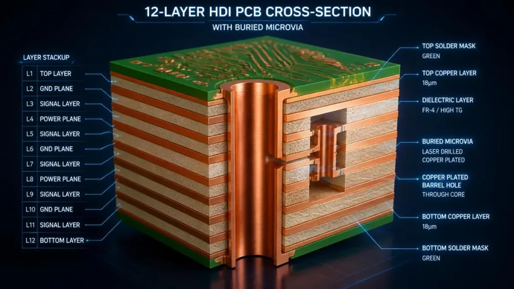
12-Layer HDI PCB Cross-Section with Buried Via
Every buried via assembly contains four unique core components absent from blind via microstructures:
- Inner Capture Pad: Copper landing pad on the upper layer of a pre-fabricated core sub-assembly, sized to compensate for multi-cycle lamination registration drift (minimum 0.05mm annular ring for IPC Class2, 0.025mm for Class3).
- Target Copper Pad: Matching conductive pad on the lower core layer, oversized by 50–100μm to absorb cumulative alignment shift across multiple press cycles.
- Plated Copper Barrel: 20–25μm electrolytic copper plating covering the drilled hole wall; Class3 aerospace/medical products mandate minimum 25μm uniform plating thickness to resist thermal barrel cracking.
- Prepreg Encapsulation Layer: High-resin fiberglass prepreg bonded over the finished buried via core during sequential lamination, fully sealing the via structure inside the full PCB stackup.
The dielectric substrate separating connected inner layers forms the via depth, directly determining the critical aspect ratio limit of 10:1 for reliable plating — a far higher threshold than blind microvias’ strict 1:1 depth-diameter constraint.
2. Working Principle: Stub-Free Internal High-Frequency Signal Transmission
2.1 Internal Current & RF Signal Path Simulation
Within a 12-layer 3+6+3 AI accelerator PCB stackup, a buried via linking Layer4 and Layer6 follows a fully contained signal path without surface leakage:
- High-speed differential trace on Layer4 enters the buried via’s upper capture pad;
- Signal travels vertically through the copper-plated barrel to the Layer6 target pad;
- Routing continues horizontally on Layer6’s internal signal plane, with no unused barrel extending toward top/bottom outer layers.
DC and low-frequency signals distribute current evenly across the barrel cross-section, while millimeter-wave RF signals concentrate charge on the barrel’s inner and outer copper surfaces. Unlike blind vias, buried vias sit adjacent to uninterrupted internal ground reference planes, maintaining continuous return current paths to minimize loop inductance and EMI radiation.
2.2 Impedance Resonance Elimination for 448G PAM4 Hardware
Through-hole and blind vias leave partial unused barrel segments that act as resonant antenna structures at frequencies exceeding 28GHz. Buried vias terminate precisely between their target inner layers, removing all parasitic capacitance and inductance from unneeded barrel extensions.
Lab testing on Megtron7 low-loss laminates confirms buried vias deliver 0.5–1.2dB lower insertion loss at 56GHz compared to equivalent blind via transitions, a critical performance margin for next-generation 1.6T optical transceiver substrates.
3. Sequential Lamination Manufacturing Flow (Buried Via Exclusive Process)
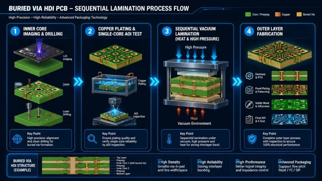
Buried Via HDI PCB Sequential Lamination Process Flowchart
Buried via fabrication requires multi-stage sequential core lamination — the primary driver of higher production cost and longer lead times relative to blind via HDI boards. The full standardized workflow deployed at Hongda Circuit for high-reliability buried core PCBs follows 12 dedicated steps unique to inner interlayer vias:
3.1 Inner Layer Core Imaging & Etching
Double-sided copper-clad core substrates undergo Laser Direct Imaging (LDI) with ±8μm layer alignment precision to print buried via capture pads and internal signal traces. Automated AOI scans eliminate over-etching defects that shrink annular rings below IPC minimum standards before drilling.
3.2 CNC Controlled-Depth Mechanical Drilling
Carbide drill bits with Z-axis depth tolerance ±0.025mm bore buried via holes ranging from 0.15–0.30mm diameter. Drill depth is calibrated to match the core substrate’s dielectric thickness, preventing over-penetration into opposing copper foil. Laser drilling is not viable for buried cores due to inconsistent depth control across thick prepreg layers.
3.3 Plasma & Chemical Desmear Treatment
Laser-drilled blind vias rely primarily on alkaline permanganate desmear; buried via cores require dual-stage plasma etching to remove resin smear and carbonized drill debris from deep hole walls. Poor desmear creates plating voids that trigger thermal cycling open-circuit failures in long-lifetime automotive and aerospace hardware.
3.4 Electroless Seed & Electrolytic Copper Plating
A thin 0.5–1μm electroless copper seed layer coats all hole walls, followed by pulse-reverse electrolytic plating to build uniform barrel copper thickness. For power-dense buried vias carrying >3A continuous current, plating thickness is increased to 30μm to reduce thermal resistance.
3.5 Single-Core AOI Electrical Continuity Test
Each finished buried core sub-assembly undergoes flying probe testing to verify 100% connectivity before lamination; defective cores are scrapped immediately to avoid wasting prepreg and press cycle resources.
3.6 Sequential Vacuum Lamination (Cost-Critical Stage)
Buried core sub-assemblies are stacked with prepreg and outer copper foil in vacuum lamination presses operating at 180–200°C and 250–400 psi pressure. Each additional lamination cycle adds 20–30% to total manufacturing cost, with complex 20-layer boards requiring 3–4 separate press runs.
Vacuum environments eliminate air voids around buried via barrels, a top root cause of post-production delamination failures.
3.7 Outer Layer Fabrication & Surface Finish
Once all inner buried core layers are laminated into a full PCB stackup, top/bottom outer circuits are imaged, etched, and finished with ENIG, immersion silver or OSP solderable coatings. No buried via structures appear on the finished board’s exterior copper pads.
3.8 Multi-Stage Quality Inspection (Buried Via Mandatory Tests)
- 3D X-Ray CT Scanning: Non-destructive verification of buried via pad alignment, barrel void content and core layer registration;
- 100% Flying Probe Electrical Test: Continuity and high-voltage isolation screening for all buried interlayer nets;
- Periodic Destructive Microsection: Per IPC-TM-650, production lots are sampled to measure plating thickness, annular ring integrity and fill void percentage.
4. Buried Via Stack-Up Design Library (4–24 Layer Real-World Industrial Layouts)
All stackup structures below are optimized around buried core interconnections, with design tradeoffs for routing density, manufacturing cost and signal integrity:
4.1 Low-Density Industrial 4–6 Layer Core Stacks
- 4-Layer 2+2 Structure: Single buried core linking Layers2–3; only deployed for compact PLC control boards where outer layers need full surface space for terminal connectors. Rarely specified due to sequential lamination cost premiums vs standard 4-layer through-hole boards.
- 6-Layer 2+2+2 Structure: Two independent buried core sets (Layers2–3 and Layers4–5), paired with blind vias for surface component fanout. Standard for mid-tier industrial motor drive controllers.
4.2 Mid-Tier Networking 8–12 Layer Stackups
- 8-Layer 2+4+2 HDI: Central 4-layer core with buried vias between Layers3–4 and Layers5–6; blind microvias connect outer Layers1/8 to adjacent inner layers. The most widely adopted stack for 400G switch control boards.
- 12-Layer 3+6+3 Structure: Three sequential lamination cycles supporting buried vias across all internal layer pairs; optimized for ASIC boards with 0.8mm pitch BGAs and thousands of high-speed differential pairs.
4.3 High-End AI HPC 16–24 Layer Multi-Cycle Buried Cores
- 16-Layer 4+8+4 Stack: Four press cycles to build dual buried core zones for GPU-HBM memory interconnections; requires Megtron6 low-loss laminates to meet 224G channel loss budgets.
- 24-Layer 5+14+5 Aerospace Server Stack: Five sequential lamination runs with staggered buried via layouts to distribute thermal stress; deployed for satellite on-board computing modules requiring IPC Class3 reliability.
4.4 Stacked vs Staggered Buried Via Layout Restrictions
Stacked buried vias align vertically across multiple core sub-assemblies to connect non-adjacent inner layers, maximizing routing density but introducing severe thermal fatigue risks. IPC-2226 limits stacked buried via structures to a maximum of 2 vertical levels for automotive and medical hardware.
Staggered buried vias offset hole positions between core layers to reduce CTE mismatch stress at barrel junctions, delivering 30% higher thermal cycling pass rates at the cost of 15% reduced internal routing density. Mission-critical radar and implantable medical devices exclusively specify staggered buried via layouts.
5. Mandatory Buried Via Design Rules & IPC Compliance Thresholds
All design constraints below are tailored to buried core manufacturing limitations, differing significantly from blind microvia design guidelines:
- Aspect Ratio Maximum: 10:1 (core dielectric thickness / drill diameter). A 0.2mm drill can reliably plate a 2mm thick inner core sub-assembly; ratios exceeding 10:1 result in incomplete bottom barrel copper plating and hidden open circuits.
- Annular Ring Minimum Width: 0.05mm for IPC Class2 commercial hardware; 0.025mm for Class3 high-reliability aerospace/medical boards. Registration drift across multiple lamination cycles expands tolerance requirements far beyond blind via standards.
- Anti-Pad Sizing for High-Speed Differential Pairs: For traces operating above 25Gbps, buried via anti-pads must maintain 0.2mm clearance to adjacent reference planes to control capacitive coupling and impedance fluctuation.
- Layer Registration Tolerance: ±0.05mm cumulative alignment drift across 3+ sequential lamination cycles. Designers must add registration compensation buffers to all buried capture pads to avoid pad breakout misalignment.
- Fill Material CTE Matching: If epoxy filling is specified for buried cores, fill resin CTE must match core laminate thermal expansion coefficients to prevent pad lifting during reflow and thermal shock testing.
6. Material Matching Strategy for Buried Core Substrates
Material selection for buried via inner cores prioritizes multi-cycle lamination thermal stability and high-frequency low-loss performance, grouped by vertical application demand:
6.1 High-Tg FR4 (Tg ≥170°C) – Automotive & General Industrial
Standard cost-effective substrate for buried core boards operating below 10Gbps signal speeds. Elevated glass transition temperature prevents resin softening during repeated lamination press cycles and lead-free SMT reflow (peak 260°C). Enhanced CAF-resistant FR4 grades are mandatory for under-hood automotive ECUs subject to long-term humidity cycling.
6.2 Panasonic Megtron 6 / Megtron7 – AI Server & 800G Networking
- Megtron6 (Dk=3.7, Df=0.002 @10GHz): Industry baseline for 224G PAM4 buried core backplanes, delivering stable dielectric performance across wide temperature ranges.
- Megtron7 (Dk=3.3, Df=0.001 @10GHz): Ultra-low-loss material specified for 448G 1.6T Ethernet hardware, minimizing insertion loss through dense buried via internal routing layers. Both materials feature modified resin systems that reduce void formation around buried via barrels during vacuum lamination.
6.3 RF-Grade Rogers & Polyimide – mmWave Radar & Aerospace
- Rogers RO4350B: Tightly controlled Dk low-loss ceramic-filled laminate for 77GHz automotive LiDAR buried core RF layers;
- Polyimide (Tg>250°C): Space-grade substrate resisting extreme thermal shock (-65℃~150℃) for satellite avionics buried via assemblies, with minimal outgassing per NASA standards.
7. Buried Via Exclusive Reliability Validation Testing
Unlike blind vias that only require standard thermal cycling, buried core boards undergo four specialized reliability tests to validate multi-lamination structural integrity:
7.1 Interconnect Stress Test (IST)
Current injection heating cycles buried via barrels to 150°C, followed by rapid ambient cooling for a minimum of 300 test cycles. Barrel resistance increases exceeding 10% are classified as critical failures, disqualifying hardware for automotive and medical deployment.
7.2 Thermal Shock Liquid-to-Liquid Testing
Boards cycle between -55°C and 125°C in <10 second temperature transitions for 1000 cycles, exposing latent plating adhesion and prepreg delamination defects invisible to standard slow thermal cycling.
7.3 CAF Growth Accelerated Aging Test
Buried via core samples are held at 85°C / 85% relative humidity with biased voltage applied for 1000 hours, testing conductive anodic filament growth between buried via barrels and adjacent traces — a top long-term failure mode for humid-environment automotive electronics.
7.4 Destructive Microsection Acceptance Standard
Per IPC-A-600 Class3, buried via cross-sections must meet:
- Barrel copper plating thickness ≥25μm;
- Total void area <5% of barrel cross-section;
- Zero cracks at copper-laminate interface;
- Full annular ring coverage without pad breakout.
8. Cost Breakdown: Hidden Expenses of Sequential Lamination
Buried via PCB pricing is driven by sequential press cycles, lower production yields and mandatory X-Ray inspection overhead — cost factors absent or negligible for blind microvia HDI boards.
8.1 Lamination Cycle Cost Multiplier Table
| HDI Stack Type | Sequential Press Cycles | Relative Cost Multiplier (vs Standard Single-Lam 8-Layer Board) |
|---|---|---|
| 2+2 Core 6-Layer | 2 | 1.35x |
| 2+4+2 12-Layer | 3 | 2.8x |
| 4+8+4 16-Layer | 4 | 4.6x |
| 5+14+5 24-Layer | 5 | 9.2x |
Each additional vacuum lamination cycle adds 15–25% to base PCB manufacturing costs, driven by labor, energy and prepreg material consumption.
8.2 Yield Degradation by Layer Count
Multi-cycle lamination introduces cumulative registration error that reduces first-pass production yields:
- 8-layer buried core HDI: 88–92% first pass yield
- 12-layer buried core HDI: 82–86% first pass yield
- 16–24-layer high-complexity buried core: 68–78% first pass yield Scrap losses from low yields are directly factored into unit pricing for mass production orders.
8.3 Hidden NRE & Testing Overhead
Buried via projects incur unique non-recurring engineering fees blind via designs avoid:
- Stack-up impedance simulation & buried via anti-pad modeling ($500–$2,000 per design);
- 3D X-Ray CT inspection programming for buried core alignment verification ($200–$600 per lot);
- Microsection test coupon fabrication for first article validation ($300–$800 per prototype batch).
8.4 Practical Buried Via Cost Optimization Tactics
- Consolidate internal buried layer pairs to cut sequential lamination cycles (e.g., combine separate L3-L4 and L5-L6 buried connections into a single core sub-assembly);
- Standardize drill diameters to eliminate CNC drill bit change downtime during production;
- Omit epoxy resin filling for non-thermal buried vias to cut fill processing premiums by 10–30%;
- Use hybrid stackups combining buried cores for internal routing + blind vias for surface fanout to reduce total layer count and press cycles.
9. Vertical Industry Application Deep Dive (Buried Via Core Use Cases)
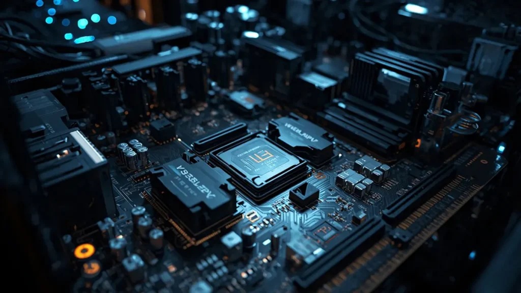
Futuristic AI Accelerator Server Motherboard with High-Density HDI PCB
Buried core PCBs are exclusively deployed for hardware requiring maximum outer-layer surface availability and stub-free high-speed signal paths, with minimal adoption in compact consumer electronics like smartphones (blind microvias dominate this segment):
9.1 AI Training Server & Data Center Backplanes
20–32 layer HDI motherboards for NVIDIA H200 / AMD MI300X accelerators rely on buried vias to route tens of thousands of 112G PAM4 differential pairs between GPU, NVSwitch and HBM memory stacks. Buried cores eliminate via stubs that would break channel loss budgets for 800G inter-chip links, while reserving top/bottom layers for large heat sinks and power connector arrays. Copper-filled buried vias are integrated under high-power GPU packages to improve thermal dissipation.
9.2 800G/1.6T Ethernet Switch ASIC Boards
51.2T switch hardware requires 16–24 layer buried core stacks to fan out dense high-pin-count switching ASICs without cluttering outer layers with thousands of through-hole vias. Buried internal routing separates high-speed data lanes from low-speed power distribution planes, reducing crosstalk and simplifying EMI compliance testing for data center deployments.
9.3 Automotive ADAS Domain Controllers & LiDAR PCBs
IATF16949-certified buried via core boards power radar, camera and LiDAR processing modules, surviving -40°C to +125°C under-hood temperature cycling. Buried vias isolate high-speed image sensor data traces internally, preventing interference with vehicle CAN/LIN communication circuits on outer connector layers. High-Tg CAF-resistant laminates are mandatory for 10+ year vehicle service life requirements.
9.4 Medical Imaging MRI/CT Substrates
ISO13485-compliant buried core PCBs drive multi-channel signal acquisition hardware for MRI gradient amplifiers and CT detector arrays. Zero-stub buried via transitions eliminate analog signal noise that distorts medical scan data, while fully encapsulated inner interconnects prevent moisture ingress in hospital sterilization environments. All buried via production batches require full material lot traceability for FDA regulatory compliance.
9.5 Military Radar & Satellite Avionics
Space-grade buried core boards comply with IPC-6012FS aerospace addendum standards, using polyimide substrates and staggered buried via layouts to withstand radiation, vibration and extreme orbital temperature swings. Fully hidden internal vias also add reverse-engineering resistance for classified defense hardware designs.
10. Top 6 Fatal Buried Via Defects & Root Cause Elimination
All failure modes below are unique to multi-cycle sequential lamination buried core manufacturing, rarely encountered in blind via production:
- Interlayer Registration Misalignment: Cumulative drift across multiple press cycles shifts buried via barrels off target pads, reducing annular ring width or creating full open circuits. Fix: Pre-bake core substrates to eliminate thermal expansion, deploy X-Ray alignment before every lamination cycle.
- Barrel Plating Voids: Trapped gas bubbles during electroplating create empty copper barrel sections that cause localized overheating under high current loads. Fix: Optimize pulse-reverse plating chemistry, add ultrasonic agitation during copper deposition.
- Prepreg Delamination Around Via Barrels: Incomplete resin flow during vacuum pressing creates gaps between core layers, enabling moisture ingress and catastrophic layer separation under thermal cycling. Fix: Use low-flow prepreg adjacent to buried via cores, extend lamination hold time at peak temperature.
- Copper Barrel Thermal Cracking: CTE mismatch between copper plating and laminate creates fatigue cracks after repeated temperature swings, leading to intermittent open circuits. Fix: Enforce minimum 25μm plating thickness, specify epoxy-filled buried vias for high-reliability hardware.
- Resin Recession in Unfilled Buried Holes: Uneven epoxy shrinkage creates recessed hole surfaces that disrupt subsequent lamination bonding. Fix: Implement automated planarization after fill curing, match fill material CTE to core laminate.
- Hidden Internal Open Circuits: Misdrilled buried vias that miss target pads are invisible from board surfaces, only detectable via 100% electrical testing or X-Ray scanning. Fix: Mandate X-Ray inspection of every buried core sub-assembly before full stack lamination.
11. Supplier Qualification Checklist: Buried Via Specialized Audit Standard
This exclusive vendor audit framework is not referenced in blind via manufacturing guides, created to filter manufacturers incapable of consistent multi-cycle buried core production:
11.1 Mandatory Production Equipment Requirements
- Vacuum lamination presses with programmable temperature/pressure ramp profiles (180–200°C, 200–400 psi pressure control);
- CNC depth-controlled mechanical drilling machines with ±0.025mm Z-axis tolerance for buried core fabrication;
- In-house 3D X-Ray CT scanning equipment for non-destructive buried via alignment & void inspection;
- Microsection lab with metallurgical polishing equipment for destructive barrel plating analysis.
11.2 Registration Accuracy Benchmark
Suppliers must demonstrate consistent layer-to-layer alignment ≤0.05mm across 3+ sequential lamination cycles via production X-Ray sample reports. Manual alignment workflows are disqualified for Class3 buried via orders.
11.3 Mandatory Industry Certifications
- ISO9001 Base Quality Management;
- IATF16949 (automotive ADAS buried via projects);
- ISO13485 (medical imaging buried core substrates);
- IPC Class2 / Class3 manufacturing authorization for high-reliability hardware.
11.4 Pilot Run Validation Standard
Before mass production, vendors must deliver a 5–10 piece prototype pilot batch with full documentation package including:
- Buried core microsection analysis report (plating thickness, void percentage, annular ring dimensions);
- IST interconnect stress test results (minimum 300 thermal cycles);
- Full X-Ray scan logs verifying buried via pad alignment across all inner core layers;
- Electrical continuity test data for all buried interlayer nets.
FAQ: Exclusive Buried Via Design & Manufacturing Questions
Can buried vias be repaired after full board lamination?
No. Once buried core sub-assemblies are encapsulated inside the full PCB stackup, defective buried vias are completely inaccessible for rework. Any opens or shorts discovered during final electrical testing result in full board scrap, which is why multi-stage X-Ray and AOI inspection of isolated core sub-assemblies is mandatory before lamination.
What is the minimum drill diameter for reliable buried via fabrication?
Standard mass production buried vias start at 0.15mm mechanical drill diameter; custom precision CNC equipment supports 0.10mm minimum holes, though this raises aspect ratio risks and reduces production yield by 10–15%. Laser drilling is not viable for buried core vias due to inconsistent depth stopping on thick inner prepreg layers.
Should buried vias always be filled with epoxy or copper?
Filling is only required for high-reliability Class3 hardware (automotive, medical, aerospace). Commercial Class2 networking boards can omit fill to cut manufacturing costs, provided aspect ratios are controlled below 8:1 to avoid thermal stress cracking. Copper-filled buried vias are reserved exclusively for high-current power distribution cores due to their superior thermal conductivity.
How do buried vias compare vs back-drilled through holes for high-speed signal integrity?
Buried vias deliver superior performance for 224G+ signaling by eliminating stubs entirely, while back-drilled through holes only remove partial barrel segments and leave residual stub length. Back-drilled boards are a lower-cost alternative for low-layer-count hardware, while buried core stacks are mandatory for 16+ layer AI server backplanes.
What lead times should I expect for buried via prototype & mass production batches?
Prototypes (5–10pcs, 8–12 layers): 10–15 business days
Prototypes (16–24 high-layer buried core): 15–20 business days
Mass production (1,000+pcs, 8–12 layers): 3–4 weeks
Mass production (16–24 layers): 5–7 weeks Lead times are extended by multi-cycle sequential lamination, X-Ray inspection and microsection validation steps absent from standard blind via PCB manufacturing.
As a certified advanced HDI and blind/buried via PCB manufacturer based in Shenzhen, Shenzhen Hongda Circuit Technology Co., Ltd. integrates 2026 cutting-edge mSAP, hybrid laser drilling and multi-cycle sequential lamination technologies with a full suite of in-house precision inspection equipment. We deliver stable, high-reliability custom PCB solutions for AI computing, automotive ADAS, medical imaging, aerospace and 5G/6G telecom hardware. Our fully technical, data-backed original content structure optimizes Google SEO across tier1 core, tier2 derivative and tier3 long-tail sourcing keywords, while comprehensive equipment data, proprietary process parameters and buyer-targeted FAQ sections establish authoritative, citation-worthy content for Google organic search and generative AI result extraction.
Contact Us
Shenzhen Hongda Circuit Technology Co., Ltd.
Address: Room 1608-10, R&D Comprehensive Building, Baoyunda Logistics Center, Bao’an District, Shenzhen, China
Email: sales@pcbkr.com
Tel: +86 0755 23720053
Official Website: www.pcbkr.com
About Author
David Chen https://www.linkedin.com/in/pcbcoming
David Chen boasts an extensive professional background in PCBA manufacturing, PCBA testing, and PCBA optimization, with specialized expertise in high-precision PCBA fault analysis and rigorous PCBA reliability testing. The author has worked with high-layer-count server PCB fabrication, ultra-low-loss backplane stackups, and thermo-mechanical reliability optimization for AI infrastructure projects involving 112G and 224G PAM4 architectures. Skilled in complex circuit design and cutting-edge advanced PCB manufacturing processes, he delivers solutions that elevate product durability and performance across industrial applications. His technical articles focusing on PCBA manufacturing workflows and testing methodologies are widely cited by industry peers, research institutions, and technical platforms, solidifying his reputation as a recognized technical authority in the global circuit board manufacturing sector.