PCB Trace Impedance Control 101: From Theory to Layout Practice
1. Introduction: Why Impedance Control Is a Must for High-Speed PCBs
PCB Impedance Control Service has become a fundamental requirement in modern high-speed electronics manufacturing, where trace design directly dictates signal integrity.
In early low-speed circuits, a PCB trace was viewed simply as a “copper wire,” with engineers focusing almost entirely on current conductivity and power handling capabilities. However, as modern signal edge rates push well into the multi-gigahertz regime, trace behavior changes fundamentally—a simple copper trace transitions into a high-frequency transmission line.
When a high-speed signal propagates along a board, any sudden variation in the trace’s characteristic impedance ($Z_0$) forces a portion of the signal energy to reflect back toward the driver, analogous to light reflecting off an impedance-discontinuity mirror. These unwanted reflections lead to signal ringing, severe overshoot, undershoot, and ultimate data degradation leading to bit errors.
Therefore, a professional PCB Impedance Control Service focuses on maintaining a tight, predictable characteristic impedance along the entire signal path—from transmitter package to substrate to receiver—ensuring clean eye diagrams, robust signal transmission, and long-term hardware reliability.
2. What Is Impedance Control in a PCB Trace? Two Perspectives
Unlike DC resistance (which depends only on copper geometry), characteristic impedance (Z₀) is a dynamic parameter determined by the capacitance, inductance, and dielectric environment surrounding the trace. Impedance control must be understood from two dimensions:
2.1 Physical / Structural Dimension: Getting the Dimensions Right
Impedance control is first and foremost a manufacturing precision problem. It requires holding trace width (W), copper thickness (T), dielectric thickness (H), and dielectric constant (Dk) within tight windows so that the fabricated cross-section produces the target Z₀.
Four Key Parameters:
- W (Trace Width): Wider trace → higher capacitance → lower impedance
- H (Dielectric Thickness): Thicker dielectric → lower capacitance → higher impedance
- T (Copper Thickness): Thicker copper → slightly higher capacitance → slightly lower impedance
- Dk (Dielectric Constant): Higher Dk → higher capacitance → lower impedance
💡 Analogy: Impedance control is like making a uniform water pipe. If one section suddenly becomes wider or narrower, the water flow (signal) will create turbulence (reflection) at that point.
2.2 Electrical / Signal-Integrity Dimension: Continuity Along the Path
Even if a single trace is manufactured to exactly 50 Ω, electrical impedance control still fails if the path contains discontinuities such as via stubs, 90° corners, or reference-plane gaps. Therefore, a fabricator must do more than etch accurate traces—they must validate the finished board with TDR (Time Domain Reflectometry) to prove continuity from the BGA pad to the connector.
3. Microstrip vs. Stripline: Structural and Electrical Comparison
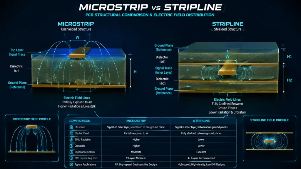
Microstrip vs. Stripline: Structural Comparison and Electric Field Distribution
| Parameter | Microstrip | Stripline |
| Structure | Outer layer trace with one reference plane below | Inner layer trace sandwiched between two reference planes |
| Field Distribution | Partly in PCB substrate, partly in air | Fully contained within the dielectric |
| Propagation Speed | Faster (lower effective Dk) | Slower (higher effective Dk) |
| EMI / Shielding | Radiates outward, susceptible to interference | Fully shielded, low EMI |
| Fabrication Complexity | Simple, lower cost | Requires more layers, slightly higher cost |
| Typical Use | RF signals, antenna traces, probe points | High-speed differential pairs, EMI-sensitive designs |
Selection Guidelines:
- RF signals, antenna traces, debug probe points → Prefer microstrip (outer layer, easy to test)
- USB, PCIe, Ethernet, and other high-speed differential pairs → Prefer stripline (inner layer, better immunity)
4. What Determines Characteristic Impedance?
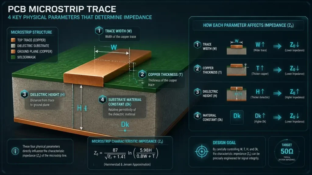
PCB Microstrip Trace: 4 Key Physical Parameters Determining Impedance (Z0)
The following table summarizes how each parameter relates to impedance and where manufacturing sensitivity lies:
| Parameter | Relationship to Impedance | Manufacturing Sensitivity |
| Trace Width (W) | Inverse: wider → lower Z₀ | 0.5 mil etch undercut can shift Z₀ by 3–5% |
| Dielectric Thickness (H) | Direct: thicker → higher Z₀ | Prepreg resin flow variation causes layer-to-layer drift |
| Copper Thickness (T) | Inverse: thicker → slightly lower Z₀ | Copper uniformity affects final trace geometry |
| Dielectric Constant (Dk) | Inverse: higher Dk → lower Z₀ | FR-4 Dk varies with frequency and temperature; high-speed designs need stable substrates |
Common Substrate Choices:
- General digital circuits (< 5 GHz): Standard FR-4 (Dk ≈ 4.2–4.5) is sufficient
- High-speed digital / RF (> 5 GHz): Use low-loss materials (e.g., Rogers RO4350B, Panasonic Megtron 6/8) for stable Dk and lower insertion loss
5. Single-Ended vs. Differential Impedance: Common Interface Standards
5.1 Basic Concepts
- Single-Ended Impedance (Z₀): The impedance of one signal trace relative to its reference plane (usually ground).
- Differential Impedance (Zdiff): The impedance between a tightly coupled pair of traces (P and N). Differential pairs require matched length, matched spacing, and the same routing layer, with an uninterrupted reference plane beneath.
5.2 High-Speed Interface Impedance Quick Reference
| Interface | Impedance Mode | Typical Target | Key Notes |
| RF / General high-speed | Single-ended | 50 Ω | RF industry standard; balances power handling and attenuation |
| USB 2.0 / USB 3.x | Differential | 90 Ω | Requires tight coupling; trace spacing dominates Zdiff |
| PCIe (Gen1–Gen6) | Differential | 85 Ω / 100 Ω | Common design values are 85 Ω or 100 Ω; follow chip datasheet |
| Ethernet (1G–100G) | Differential | 100 Ω | IEEE 802.3 mandates 100 ± 10% Ω; premium shops hold ±5% |
| HDMI / DisplayPort | Differential | 100 Ω | Vias and connector launches are common discontinuity sources |
| DDR4 / DDR5 Address/Command | Single-ended | 40 Ω | Address/command groups typically use 40 Ω single-ended |
| DDR4 / DDR5 Clock / DQS | Differential | 80–100 Ω | Data strobe and clock lines use differential routing |
| SATA / SAS | Differential | 100 Ω | — |
| MIPI DSI/CSI | Differential | 100 Ω | Common in camera and display interfaces |
Note: Differential pairs require not only impedance control but also length matching (phase matching). Typically, the length difference between P and N should be less than 5 mil (0.127 mm); otherwise, common-mode noise will be generated.
6. Layout Pitfall Guide: Reference Planes and Split Crossings
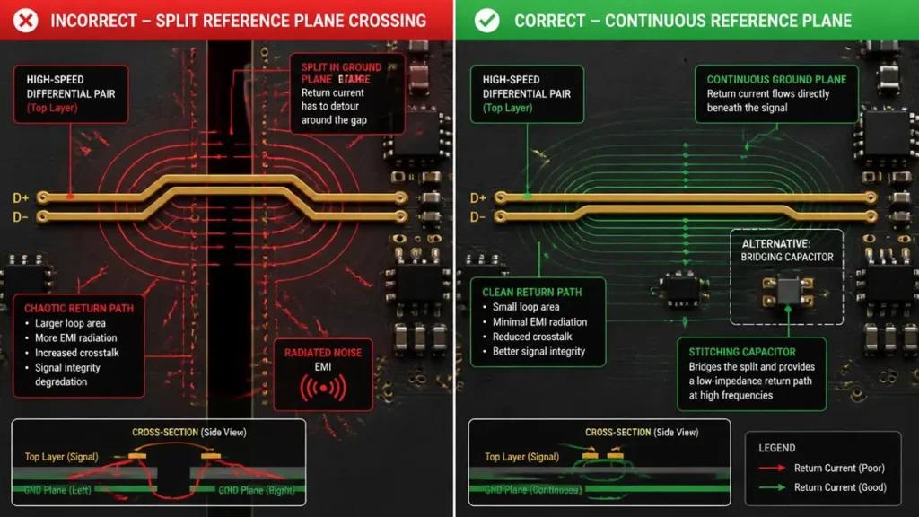
PCB Layout Pitfall: Split Reference Plane Crossing vs. Continuous Ground Return Path
Impedance control starts with the designer, not just the fabricator. Below are the most common layout traps that cause impedance failure and how to avoid them.
6.1 Keep Reference Planes Intact: Never Cross a Split
Problem: If the reference plane (ground or power) beneath a high-speed trace has a split, slot, or void, the return current path is broken. This causes an impedance discontinuity and severe EMI issues.
Solutions:
- Ensure continuous reference planes beneath all high-speed traces, especially differential pairs.
- If crossing a power-plane split is unavoidable, place a stitching capacitor (0.1 µF or 1 µF) at the crossing point to bridge the return current path.
- Avoid routing traces across the edges of plane layers or over long slots in planes.
6.2 Differential Pair Routing Rules
| Rule | Explanation |
| Length Matching | Keep P/N length difference within 5 mil; for high-speed interfaces (e.g., PCIe Gen4+), aim for within 2 mil |
| Constant Spacing | Maintain uniform spacing between the pair; avoid “tight-then-loose” routing |
| Same Layer Routing | Route the pair on the same signal layer to avoid impedance discontinuities from layer changes |
| Symmetrical Layer Change | If layer change is necessary, swap both P and N together and place a ground via adjacent to the transition vias |
6.3 Avoid 90° Corners
Problem: A 90° corner effectively increases trace width at the bend (behaving more like a square than a rectangle), causing a local impedance drop and parasitic capacitance.
Solution: Use 45° mitered corners or arc corners for all high-speed traces.
6.4 Via Stub Control
Problem: When an inner-layer trace changes layers, the unused portion of the via forms a “stub.” At high speeds, this stub acts as a capacitive load, causing an impedance dip.
Solutions:
- For speeds ≥ 5 Gbps, use backdrilling to remove unused via stubs.
- Alternatively, optimize the stackup so signals transition between adjacent or nearby layers (e.g., L1→L2 or L1→L3) to minimize stub length.
6.5 EMI Considerations for Outer-Layer Microstrips
Microstrip traces on outer layers radiate electric fields into the air. For long high-speed traces on the surface:
- Add ground guard traces on both sides, with ground vias stitched at regular intervals.
- Route sensitive high-speed traces on inner stripline layers whenever possible.
7. How to Collaborate with Your PCB Fabricator
Impedance control is a two-way street between design and manufacturing. Here are the key collaboration steps:
7.1 Issuing an Impedance Requirements Table
At the design stage, provide your fabricator with an impedance control requirements table containing at least the following:
| Item | Example |
| Board Thickness / Layer Count | 1.6 mm / 8 layers |
| Interface Types | USB 3.0, PCIe 3.0, DDR4 |
| Impedance Mode | Single-ended / Differential |
| Target Impedance | 90 Ω ±10% (diff), 50 Ω ±10% (SE) |
| Preferred Routing Layer | Inner layer (stripline) or outer layer (microstrip) |
| Substrate Requirement | FR-4 / Low-loss material (e.g., Megtron 6) |
| Copper Weight | Inner 1 oz / Outer 1 oz |
| Surface Finish | ENIG (recommended for high-speed) |
7.2 Stackup Review (Stackup Confirmation)
Impedance is not calculated in isolation—it is defined by the stackup. Before freezing your layout, have the fabricator issue a stackup confirmation table based on their material library, specifying:
- Thickness of each Core / Prepreg layer
- Corresponding Dk values
- Calculated trace width / spacing for each impedance target
Recommendation: Do not rely solely on online impedance calculators. Different fabricators use substrates with slightly different Dk values and lamination processes. Always use the stackup table confirmed by your specific fabricator.
7.3 Acceptance: Always Request Test Reports
When receiving production boards, require the fabricator to provide:
- Stackup drawing (with dielectric thicknesses and material declarations for each layer)
- Impedance test report (TDR curves showing measured vs. target values)
- Impedance coupon location map (proving coupons were placed on every production panel, not just qualification samples)
8. Frequently Asked Questions (FAQ)
Why is 50 Ω the standard impedance in RF and high-speed design? Why not 60 Ω or 40 Ω?
The prevalence of 50 Ω is not arbitrary—it is the result of historical standardization and physical optimization:
Trade-off between power and loss: In coaxial cables, calculations show:
77 Ω yields minimum signal attenuation (best for long-distance transmission)
30 Ω yields maximum power capacity
50 Ω is approximately the geometric mean of these two values, representing a practical engineering compromise between transmission efficiency and power handling.
Mechanical manufacturability: A 50 Ω air-dielectric coaxial cable has a center-conductor-to-shield diameter ratio of roughly 2.3:1, a dimension that is mechanically easy to produce and physically robust.
Industry standardization: After World War II, the U.S. military and telecommunications industry adopted 50 Ω as the standard. It subsequently became the universal impedance for RF test equipment, connectors, and coaxial cables—a convention that persists today.
Therefore, unless there are specific power or sensitivity constraints, RF traces and test equipment universally default to 50 Ω single-ended impedance.
What is PCB trace impedance control, and why is it necessary for high-speed circuits?
Definition: Characteristic impedance (Z0) is a dynamic electrical parameter determined by the capacitance, inductance, and dielectric environment surrounding a trace. Impedance control means keeping the characteristic impedance constant and predictable across the entire signal path.
Necessity: As signal speeds reach the gigahertz range, traces stop acting like simple wires and become transmission lines. Any sudden impedance change along the path causes signal energy to reflect back to the source, creating ringing, overshoot, and undershoot, which can directly cause bit errors.
What are the main physical parameters that determine PCB trace characteristic impedance?
Characteristic impedance is primarily governed by four physical parameters:
Trace Width (W): Inversely related—wider traces increase capacitance, resulting in lower impedance.
Dielectric Thickness (H): Directly related—thicker dielectrics decrease capacitance, resulting in higher impedance.
Copper Thickness (T): Inversely related—thicker copper slightly increases capacitance, slightly lowering impedance.
Dielectric Constant (Dk): Inversely related—higher Dk increases capacitance, resulting in lower impedance.
What are the differences between Microstrip and Stripline, and how do I choose between them?
Structural and Electrical Comparison:
Microstrip: An outer-layer trace with a single reference plane below it. Fields are split between the substrate and air, offering faster propagation speeds but higher radiation/interference susceptibility at a lower manufacturing cost.
Stripline: An inner-layer trace sandwiched between two reference planes. Fields are completely contained within the dielectric, providing strong EMI shielding and noise immunity, though propagation speed is slower and fabrication cost is higher.
Selection Guidelines:
Prefer Microstrip for RF signals, antenna traces, and debug probe points.
Prefer Stripline for USB, PCIe, Ethernet, and other EMI-sensitive high-speed differential pairs.
Impedance control is not an esoteric “black art”—it is a quantifiable, verifiable engineering discipline. Understanding the difference between microstrip and stripline, knowing when to use single-ended vs. differential routing, guarding reference-plane integrity and length-matching rules during layout, and collaborating with your fabricator on stackup confirmation and TDR validation will enable you to reliably achieve target impedance in the vast majority of high-speed designs.
Remember the core principle: Impedance control starts with the stackup, is implemented in the layout, and is verified with test reports.
Company: Shenzhen Hongda Circuit Technology Co., Ltd.
Website:www.pcbkr.com
Email:sales@pcbkr.com
Phone: +86 0755 23720053
Certifications: ISO 9001:2026 | AS9100D | IPC-6012 Class 3/3A | ISO 13485 | IATF 16949
Headquarters: Room 1608-1610, Research Development Comprehensive Building, Baoyunda Logistics Center, Baoan, Shenzhen, China
About Author
David Chen https://www.linkedin.com/in/pcbcoming
David Chen boasts an extensive professional background in PCBA manufacturing, PCBA testing, and PCBA optimization, with specialized expertise in high-precision PCBA fault analysis and rigorous PCBA reliability testing. The author has worked with high-layer-count server PCB fabrication, ultra-low-loss backplane stackups, and thermo-mechanical reliability optimization for AI infrastructure projects involving 112G and 224G PAM4 architectures. Skilled in complex circuit design and cutting-edge advanced PCB manufacturing processes, he delivers solutions that elevate product durability and performance across industrial applications. His technical articles focusing on PCBA manufacturing workflows and testing methodologies are widely cited by industry peers, research institutions, and technical platforms, solidifying his reputation as a recognized technical authority in the global circuit board manufacturing sector.