Understanding Impedance Control in PCB Traces: Microstrip vs. Stripline — A Procurement & Manufacturing Guide
How to achieve controlled impedence in pcb is a critical technical question that cannot be overlooked when sourcing printed circuit boards for high-end scenarios including AI servers, 5G infrastructure, and automotive radar modules. Unlike conventional low-frequency circuit designs, a PCB trace in 2026’s high-speed electronic systems is no longer a simple copper conductor for current conduction. Instead, it functions as a professional transmission line whose electrical performance is completely dominated by electromagnetic wave mechanics.
The core of PCB impedance control lies in regulating the characteristic impedance (Z₀) of traces. Characteristic impedance refers to the dynamic voltage-current ratio generated when high-frequency signals propagate along PCB transmission lines, a key parameter that is fundamentally different from DC resistance and has no correlation with it. This vital electrical index is jointly determined by three core factors: the geometric size of the PCB trace, the dielectric properties of the substrate material, and the distance between the trace and its adjacent reference plane.
Precise impedance control is indispensable for stable operation of high-speed systems. Once the actual impedance of PCB traces deviates from the preset design target values, a series of severe signal integrity problems will occur. Typical issues include signal reflection and ringing during signal transmission, gradual closure of the signal eye diagram, and a sharp rise in the bit-error-rate (BER), which may even lead to catastrophic system failures in severe cases.
For procurement teams responsible for verifying and screening PCB suppliers, the manufacturing capability to stably maintain trace impedance within strict tolerance ranges has become the most intuitive and reliable standard to evaluate a fabricator’s overall process maturity and high-end board production capability.
What Is Impedance Control in a PCB Trace? Two Descriptions Every Buyer Must Understand
When evaluating a controlled impedance PCB manufacturer, you will encounter two distinct but complementary definitions. Both matter during supplier audits.
Physical & Structural Description
Impedance control is the deliberate engineering of trace geometry and laminate stack-up to create a transmission line with a specific target impedance. It involves controlling:
- Trace width (W) and copper thickness (T)
- Dielectric thickness (H) between signal and reference planes
- Dielectric constant (Dk/εr) of the substrate
- Surface finish planarity (critical for fine-pitch BGA pads at >10 GHz)
A fabricator achieves this by selecting precise core and prepreg thicknesses, maintaining etch uniformity, and validating the stack-up before phototooling. At Shenzhen Hongda Circuit Technology, stack-up engineering is performed with Polar Si9000e field solvers and validated against IPC-2141A approximations before the first panel enters production.
Electrical & Signal-Integrity Description
Impedance control ensures that the characteristic impedance remains constant along the entire length of the trace — what engineers call impedance continuity. Any discontinuity (a via stub, a plane split, or an uneven solder mask) creates an impedance bump. When a high-speed wave hits that bump, a portion of its energy reflects back toward the source, just like a pressure wave in a pipe hitting a sudden constriction. The result is standing waves, jitter, and EMI.
For procurement professionals, the takeaway is simple: a supplier that only quotes “50 Ω impedance” without explaining how they maintain continuity across layer transitions, via structures, and panel-wide etch uniformity is a supplier that will cost you redesign cycles.
How Trace Geometry and Material Properties Determine Impedance — Microstrip vs. Stripline in Modern PCB Manufacturing
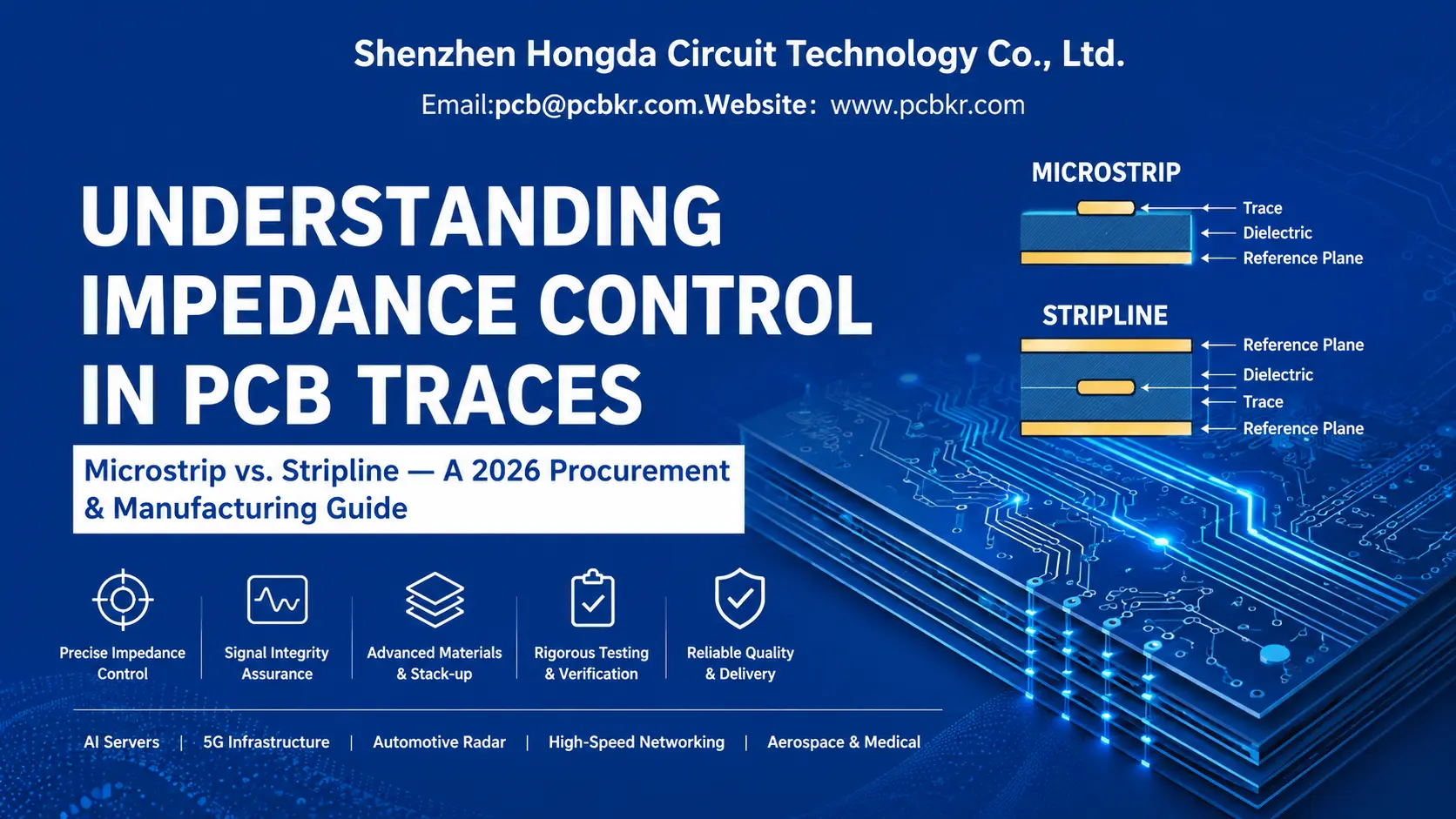
The choice between microstrip impedance control and stripline impedance control is one of the first stack-up decisions that affects both performance and unit cost. Here is how the two structures compare in 2026 high-speed designs.
Microstrip: The Outer-Layer Workhorse
A microstrip is a trace routed on an outer layer with a single reference plane beneath it. The electromagnetic field propagates partly through the PCB substrate and partly through air, yielding an effective dielectric constant lower than the base material alone.
Advantages:
- Faster signal propagation (lower effective Dk)
- Easier to manufacture and modify
- Lower layer-count cost for moderate-speed designs
Disadvantages:
- Higher radiation and EMI susceptibility
- Impedance more sensitive to solder-mask thickness and copper-etch variation
- Less shielding for sensitive RF paths
When to specify it: Short, high-speed breakout traces on AI accelerator cards; RF antenna feed lines below 6 GHz; cost-sensitive networking hardware where EMI can be managed via shielding cans.
Stripline: The Inner-Layer Precision Structure
A stripline embeds the trace between two ground planes, fully surrounded by dielectric. This creates a homogeneous electromagnetic environment.
Advantages:
- Superior EMI shielding and crosstalk suppression
- More consistent impedance because the field is entirely contained within the laminate
- Preferred for >5 GHz signals and PAM4 multilevel signaling
Disadvantages:
- Slower propagation delay (higher effective Dk)
- Narrower trace width required for the same impedance, demanding tighter etch tolerance
- Increased layer count and fabrication complexity
When to specify it: 112G/224G PAM4 backplane channels; 5G mmWave routing; automotive Ethernet and ADAS sensor interconnects where noise immunity is safety-critical.
Material Selection: Why FR-4 Is No Longer the Default
Standard FR-4 (Dk ≈ 4.2–4.5, Df ≈ 0.019–0.025) is adequate for sub-Gigabit designs. In 2026, however, AI server and telecom procurement specs routinely demand ultra-low-loss laminates:
| Material | Dk @10 GHz | Df @10 GHz | Typical Use Case |
|---|---|---|---|
| Panasonic Megtron 6/8 | ~3.4–3.7 | 0.002–0.004 | 112G/224G AI backplanes |
| Isola Tachyon 100G | ~3.0–3.3 | <0.002 | 400G/800G switching |
| Rogers RO4350B | 3.48 | 0.0037 | 5G sub-6 GHz & mmWave |
| PTFE (Teflon) | 2.2–2.6 | 0.0009–0.0025 | Microwave & radar |
Shenzhen Hongda Circuit Technology maintains certified stock of Megtron 6/8, Tachyon 100G, Rogers 4003/4350B, and RT5880, with full material traceability for aerospace and medical-grade programs. Our 2026 manufacturing data shows consistent Cpk values above 1.33 on controlled-impedance layers — exceeding typical industry benchmarks.
Single-Ended vs. Differential Impedance — Target Values & Procurement Traps
Single-Ended Impedance (Z₀)
Most RF and general-purpose digital traces target 50 Ω single-ended impedance. This value is a historical compromise between maximum power transfer (≈30 Ω) and minimum attenuation (≈77 Ω) derived from coaxial cable engineering. It remains the default for PCIe, RF front-ends, and DDR address lines.
Differential Impedance (Zdiff)
High-speed serial buses use differential pairs to reject common-mode noise. The differential impedance is not simply twice the single-ended value; it is a function of odd-mode impedance (Zodd) and coupling spacing (S):
Zdiff = 2 × Zodd
Tight coupling increases mutual inductance and lowers Zdiff, meaning trace spacing must be held as precisely as trace width.
Common Interface Targets for 2026 Designs
| Interface | Target Impedance | Tolerance |
|---|---|---|
| RF / General digital | 50 Ω SE | ±5% – ±10% |
| USB 2.0 / USB 3.x | 90 Ω diff | ±7% |
| HDMI / DisplayPort / Ethernet | 100 Ω diff | ±5% |
| PCIe Gen4/5/6 | 85 Ω diff | ±5% |
| DDR4/DDR5 data & clock | 80–100 Ω diff | ±5% |
| 224G PAM4 backplane | 100 Ω diff | ±5% or tighter |
Procurement Pitfall to Avoid: Do not accept a supplier who only tests coupons and never correlates coupon impedance to actual board traces. At Hongda Circuit, we perform automated Time-Domain Reflectometry (TDR) inline screening on production panels, not just test coupons, ensuring that the trace on your AI server board matches the coupon within ±5%.
Practical Design, Verification & Manufacturing — What High-Volume Buyers Should Audit
Stack-Up Collaboration Before Layout
Controlled impedance begins before the first trace is routed. A competent fabricator should review your preliminary stack-up and return a documented impedance table within 24 hours. Shenzhen Hongda Circuit Technology provides complimentary DFM reviews that include:
- Polar Si9000e field-solver validation
- Material substitution recommendations (e.g., Megtron 8 vs. FR-4 for 224G)
- Backdrill stub-length analysis (target: <2 mil for PAM4 channels)
- Anti-pad geometry optimization for high-speed vias
Termination Strategies & Layout Discipline
Even perfect fabrication cannot fix poor layout. Ensure your design team follows these rules:
- Never route over split planes. A broken reference plane destroys the return path and creates an inductive impedance spike.
- Place ground return vias adjacent to every signal via when changing layers.
- Match differential-pair lengths to within 20% of the signal rise time, placing serpentine corrections at the mismatch source, not the destination.
- Use 45° or arc corners instead of 90° bends to minimize capacitive discontinuities.
Manufacturing Equipment That Defines Capability in 2026
When auditing a PCB manufacturer for impedance-controlled RF and high-speed boards, verify that the facility owns and operates:
- LDI (Laser Direct Imaging): Eliminates phototool degradation that causes pad-size variation. Hongda Circuit uses SCREEN Ledia LDI for soldermask and etch resist.
- Precision Laser Drilling: Mitsubishi UV/CO₂ systems for microvias down to 0.075 mm.
- Controlled-Pressure Lamination: LAUFFER systems that prevent resin smear and maintain dielectric thickness uniformity.
- 3D X-Ray & TDR Verification: Nordson DAGE X-ray for void detection; Tektronix/Polar TDR systems for impedance validation on boards, not just coupons.
- XRF Metrology: Non-destructive gold/nickel thickness verification calibrated to NIST-traceable standards.
Backdrilling & Via Stub Management
At 56 GHz Nyquist frequencies (224G PAM4), an un-backdrilled via stub acts as a resonant antenna. Hongda Circuit’s precision Z-axis backdrilling achieves stub lengths below 2 mil, and our SI team validates anti-pad geometries with 3D full-wave electromagnetic solvers to eliminate localized impedance drops caused by parasitic capacitance.
Why Shenzhen Hongda Circuit Technology for Your Controlled Impedance PCB Programs
Sourcing high-speed PCB manufacturing with tight impedance control is a supply-chain risk decision, not merely a price decision. Here is how Hongda Circuit de-risks your program:
| Procurement Concern | Hongda Circuit Capability |
|---|---|
| Technical ceiling | 104-layer backplanes, Any-Layer HDI, mSAP fine-line, full PTFE RF, IC substrates |
| Signal-integrity validation | In-house TDR, VNA, and 3D EM simulation; Cpk >1.33 on impedance layers |
| Material security | Certified stock of Megtron 6/8, Tachyon 100G, Rogers, Isola, Taconic |
| Quality pedigree | ISO 9001:2026, AS9100D, IATF 16949, IPC-6012 Class 3/3A, ISO 13485 |
| Speed-to-market | 30-minute inquiry response, 1-hour engineering evaluation, 24/7 technical support |
| Traceability | Full-process digital simulation, AI-driven ERP tracking, material lot traceability |
We have supplied precision-controlled impedance boards for AI inference clusters, 800G switch fabrics, automotive ADAS modules, and aerospace avionics. Whether you need a prototype lot of DDR5 memory modules or volume production of 40-layer ultra-low-loss backplanes, our engineering team operates as an extension of your hardware team.
Ready to eliminate impedance risk from your next design? Submit your Gerber files, stack-up, and impedance requirements to sales@pcbkr.com. Our engineering team will return a comprehensive DFM review, material recommendation, and competitive quotation within 24 hours.and competitive quotation within 24 hours.
Procurement FAQ — What Buyers Ask When Sourcing Controlled Impedance PCB Manufacturers
How do I verify that a PCB manufacturer can actually hold ±5% impedance tolerance, not just quote it?
Demand three pieces of evidence: (1) written process-capability studies (Cpk) for impedance layers; (2) sample TDR reports from recent production runs showing actual vs. target values across multiple panels; and (3) a list of in-house metrology equipment (Polar TDR, VNA, XRF). A factory that outsources TDR testing lacks real-time process feedback. At Shenzhen Hongda Circuit Technology, we publish Cpk data and provide TDR reports with every controlled-impedance shipment
Should I specify microstrip or stripline for my high-speed design, and how does it affect cost?
Use microstrip for short breakout traces and cost-sensitive outer-layer routing below 10 GHz. Use stripline for long channels, sensitive clock lines, or any frequency above 5 GHz where EMI and crosstalk are concerns. Stripline adds 1–2 layers to the stack-up and requires tighter etch tolerance, typically increasing unit cost by 10–20%. However, the cost of a field failure due to poor signal integrity almost always exceeds the fabrication premium.
What material should I specify for 112G/224G PAM4 or mmWave 5G designs?
Avoid generic FR-4 above 5 GHz. For 112G/224G AI backplanes, specify Panasonic Megtron 6 or 8 (Dk ~3.4, Df <0.004). For 5G mmWave, Rogers RO4350B or PTFE-based laminates provide stable Dk and ultra-low loss. Always require your fabricator to use manufacturer-certified Dk/Df values at your operating frequency, not generic datasheet numbers.
How do manufacturing tolerances impact impedance, and what should my purchase order specify?
Etch width variation (±0.5–1.0 mil), dielectric thickness fluctuation (±5%), and copper-weight non-uniformity all shift impedance. Your PO should specify: (1) target impedance and tolerance (e.g., 100 Ω diff ±5%); (2) test method (TDR per IPC-TM-650); (3) coupon location on panel; and (4) required documentation (impedance report with waveform screenshots). Hongda Circuit tests on production boards, not just coupons, and guarantees impedance reports with every lot.
What is backdrilling, and when should I require it in my RFQ?
Backdrilling removes the unused portion (stub) of a plated through-hole after lamination. At frequencies above 10 GHz, via stubs create resonant impedance discontinuities and insertion-loss spikes. Require backdrilling for any high-speed digital design above 25 Gbps or RF above 10 GHz. Specify maximum stub length (e.g., <8 mil for 56G, <2 mil for 224G PAM4). Hongda Circuit offers precision backdrilling with stub control below 2 mil and validates results with 3D X-ray inspection.
Company: Shenzhen Hongda Circuit Technology Co., Ltd. Website: www.pcbkr.com Email: sales@pcbkr.com Phone: +86 0755 23720053 Certifications: ISO 9001:2026 | AS9100D | IPC-6012 Class 3/3A | IATF 16949 | ISO 13485
About Author
David Chen https://www.linkedin.com/in/pcbcoming
David Chen boasts an extensive professional background in PCBA manufacturing, PCBA testing, and PCBA optimization, with specialized expertise in high-precision PCBA fault analysis and rigorous PCBA reliability testing. The author has worked with high-layer-count server PCB fabrication, ultra-low-loss backplane stackups, and thermo-mechanical reliability optimization for AI infrastructure projects involving 112G and 224G PAM4 architectures. Skilled in complex circuit design and cutting-edge advanced PCB manufacturing processes, he delivers solutions that elevate product durability and performance across industrial applications. His technical articles focusing on PCBA manufacturing workflows and testing methodologies are widely cited by industry peers, research institutions, and technical platforms, solidifying his reputation as a recognized technical authority in the global circuit board manufacturing sector.