RO4003C vs. RO4350B: Complete Rogers PCB Material Selection Guide for RF Engineers and Procurement Teams
Choosing the right Rogers PCB material directly determines whether your high‑frequency design meets its insertion‑loss budget, passes thermal cycling qualification, and ships on time. In 2026, with 5G mmWave infrastructure expanding, 77 GHz automotive radar volumes surging, and AI‑driven RF systems demanding tighter tolerances, the debate between Rogers RO4003C and RO4350B has moved from a simple Dk/Df comparison to a procurement‑critical supply‑chain decision. This guide unpacks the electrical, mechanical, and commercial variables that separate these two workhorse laminates—and shows how a qualified Rogers PCB manufacturer turns material selection into a competitive advantage.
Understanding Rogers PCB Material Dielectric Constant and Loss Tangent in 2026
Before comparing specific grades, procurement teams and RF engineers need to align on how Rogers Corporation characterizes its laminates. Unlike standard FR‑4, where a single Dk value often suffices for stackup calculation, Rogers high‑frequency materials publish two distinct dielectric constants: Process Dk (measured under tightly controlled laboratory conditions) and Design Dk (intended for field‑solver impedance modeling).
Process Dk vs. Design Dk — Why the Difference Matters for Impedance Modeling
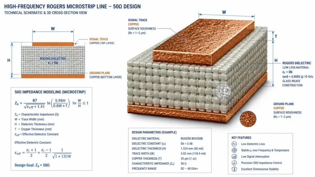
Rogers PCB Microstrip Line 3D Cross-Section & 50Ω Impedance Modeling
Rogers RO4003C carries a Process Dk of 3.38 ± 0.05 at 10 GHz, while its Design Dk sits at 3.55. RO4350B lists a Process Dk of 3.48 ± 0.05 and a Design Dk of 3.66. The gap exists because Design Dk incorporates real‑world fabrication effects—copper roughness, resin content variation, and glass‑weave interaction—that shift the effective permittivity seen by the propagating signal.
For procurement teams reviewing supplier quotes, this distinction is non‑negotiable: if your RF designer modeled traces at 3.38 but the fabricator builds using 3.55 assumptions, the resulting impedance deviation can push a nominally 50 Ω microstrip outside the ±10% tolerance band. Reputable Rogers PCB suppliers like Shenzhen Hongda Circuit Technology validate every stackup against Polar SI9000 or similar field solvers before releasing the job to production, ensuring the Design Dk used in simulation matches the manufacturing reality.
Df @ 10 GHz: How 0.0027 vs. 0.0037 Impacts Your Insertion Loss Budget
The dissipation factor—often called loss tangent or tan δ—quantifies how much signal energy converts to heat within the dielectric. At 10 GHz, RO4003C achieves Df = 0.0027, while RO4350B measures 0.0037. That 27% difference is not marginal for long trace runs or phased‑array antenna feed networks.
In a 77 GHz automotive radar PCB, for example, every 0.001 reduction in Df can translate to measurable detection‑range improvement. For a 5G NR base station operating at 28 GHz or 39 GHz, lower Df preserves SNR across the beamforming network, reducing the power amplifier overhead required to compensate for dielectric loss. When your link budget is measured in tenths of a decibel, RO4003C’s advantage becomes a system‑level performance win.
RO4003C vs. RO4350B: Head‑to‑Head Technical Comparison
Both laminates belong to Rogers’ RO4000 series, sharing a ceramic‑filled hydrocarbon matrix that processes similarly to FR‑4—no plasma activation, no special drilling parameters, no PTFE handling headaches. Yet their additive packages create divergent behavior in thermal, mechanical, and safety domains.
Dielectric Constant Stability Across 8–40 GHz Frequency Range
Rogers publishes Dk‑versus‑frequency curves showing both materials remain stable through the microwave and lower millimeter‑wave bands. RO4003C and RO4350B both exhibit minimal Dk dispersion from 8 GHz to 40 GHz, a property that simplifies wideband impedance matching.
However, the absolute offset between them—roughly 0.10 in Process Dk and 0.11 in Design Dk—means trace geometries must be recalculated when migrating from one material to the other. A 50 Ω microstrip on RO4003C requires a narrower trace than the same target on RO4350B for identical dielectric thickness. Direct substitution without re‑simulation risks mismatch, reflection, and degraded return loss.
UL 94V‑0 Flame Retardant Rating: The Deciding Factor for Safety‑Critical Applications
Here lies the most visible separator: RO4350B is UL 94V‑0 rated; RO4003C is not. RO4003C carries no flame‑retardant additive (NON FR), making it unsuitable for end products that must pass UL, CE, or automotive safety certifications.
For procurement managers sourcing PCBs for consumer electronics, automotive under‑hood modules, or medical devices, this single attribute often overrides the Df advantage of RO4003C. A 94V‑0 rating demands that the material self‑extinguish within 10 seconds after flame removal and produce no flaming drips.
If your BOM must satisfy AEC‑Q200, IEC 60695, or UL 94V‑0 flame retardant standards, RO4350B becomes the default path. RO4003C remains viable only when the system‑level enclosure or housing carries the fire‑safety burden, or when the application is exempt from vertical‑burn testing—such as base‑station antennas, satellite payloads, or laboratory test fixtures.
Z‑Axis CTE and PTH Reliability Under Thermal Cycling
Thermal expansion behavior diverges sharply between the two grades. RO4350B offers a Z‑axis CTE of 32 ppm/°C, while RO4003C measures 46 ppm/°C.
In multilayer boards with high aspect‑ratio plated through‑holes (PTH), repeated thermal cycling (−40 °C to +125 °C in automotive qualification, or −55 °C to +125 °C in aerospace) stresses the copper barrel. A lower Z‑axis CTE reduces the differential expansion between dielectric and copper, mitigating barrel cracks, corner cracks, and eventual via failure. For high‑reliability programs with long service‑life requirements, RO4350B’s thermal stability provides a tangible reliability margin.
2026 Manufacturing Trends: Rogers PCB Fabrication Technology Evolution
The Rogers material landscape in 2026 is shaped by three converging forces: mmWave frequency escalation, hybrid stackup adoption, and supply‑chain volatility. Understanding these trends helps procurement teams specify not just the right material, but the right manufacturing partner.
Hybrid Stackup Design: Combining Rogers RF Layers with FR‑4 for Cost Optimization
Pure Rogers builds deliver optimal RF performance, yet most production teams now favor hybrid stackups—Rogers laminate on outer RF/antenna layers, with standard FR‑4 or high‑Tg FR‑4 forming the inner mechanical core. This architecture cuts material cost by 30–50% while preserving signal integrity on critical traces.
Successful hybrid lamination demands precise control of resin flow, CTE matching, and copper thickness symmetry. Asymmetric builds risk warpage during reflow, while excessive resin flow can create voids at the Rogers‑FR‑4 interface. At Shenzhen Hongda Circuit Technology, hybrid Rogers‑FR‑4 stackups are processed on LAUFFER lamination systems with programmable pressure and temperature profiles, ensuring void‑free bonding and flatness within IPC‑6012 Class 3 tolerances.
Laser Direct Imaging (LDI) and Laser Drilling for mmWave Precision
As operating frequencies push past 40 GHz into 77 GHz radar and 100 GHz+ 6G research, trace‑width tolerance and via stub length become first‑order concerns. Traditional UV exposure struggles to hold ±5% impedance control on 2.5 mil lines, whereas LDI (Laser Direct Imaging) eliminates phototool distortion and achieves sub‑10 μm registration accuracy.
For via formation, UV/CO₂ hybrid laser drilling creates microvias down to 50 μm diameter—essential for Any‑Layer HDI in RF modules where real estate is constrained. Blind vias eliminate via stubs that cause insertion‑loss notches at mmWave frequencies; for 224G PAM4‑equivalent RF channels, residual stub length must stay below 5 mil.
Shenzhen Hongda Circuit Technology deploys Mitsubishi UV/CO₂ laser drilling systems and SCREEN Ledia LDI exposure across its Rogers‑capable production lines, supporting controlled‑impedance traces down to 2.5 mil with TDR verification.
Surface Finish Selection for High‑Frequency Rogers PCBs
Surface finish directly impacts RF performance at mmWave. ENIG (immersion gold) remains the default for most RF applications due to its flatness and solderability, but its nickel layer introduces magnetic loss at frequencies above 10 GHz. For 2026 mmWave 5G antenna arrays and 77 GHz radar boards, immersion silver (ImAg) is gaining traction because its surface roughness is lower than ENIG, preserving signal integrity at the conductor‑air boundary.
HASL is generally avoided above 3 GHz due to thickness variation and surface topography. For Rogers PCBs operating below 12 GHz, ENIG remains perfectly adequate; above 20 GHz, procurement teams should discuss ImAg or ENEPIG options with their fabricator.
Procurement Decision Matrix: When to Specify RO4003C vs. RO4350B
Material selection is not an isolated engineering exercise—it sits at the intersection of electrical specification, regulatory compliance, unit cost, and supply‑chain availability. Use the following framework to align your procurement strategy with design requirements.
Commercial RF Applications: Why RO4003C Delivers Better Signal Integrity per Dollar
Specify RO4003C when:
‑ Insertion loss is the dominant constraint. Cellular base station antennas, satellite communication payloads, low‑noise amplifier chains, and test‑and‑measurement fixtures all benefit from the 0.0027 Df.
‑ UL 94V‑0 is not mandated. If the end product is a base‑station remote radio unit, an outdoor antenna array, or a lab instrument where flame compliance is handled at the system or enclosure level, RO4003C eliminates the cost premium of flame‑retardant chemistry.
‑ Cost optimization matters. RO4003C typically runs 15–25% lower in raw‑material cost than RO4350B at equivalent thickness, a difference that scales meaningfully at production volumes.
‑ Halogen‑free requirements exist. RO4003C is halogen‑free; RO4350B uses brominated flame retardants. For projects targeting RoHS‑plus‑halogen‑free compliance, RO4003C simplifies environmental certification.
Automotive Radar and Aerospace: Why RO4350B Remains the Default Choice
Specify RO4350B when:
‑ UL 94V‑0 is mandatory. Automotive under‑hood electronics, consumer‑premise equipment, industrial controllers, and medical devices almost universally require V‑0‑rated substrates. RO4350B is the Rogers laminate that satisfies this without stepping up to more exotic (and expensive) alternatives like RO4835.
‑ Thermal cycling reliability is critical. The 32 ppm/°C Z‑axis CTE protects PTH integrity through thousands of temperature swings. For ADAS radar modules expected to survive 10+ years of vibration and thermal shock, this reliability margin justifies the slightly higher Df.
‑ Active RF circuits with higher power dissipation. Power amplifiers, transmit chains, and high‑reliability aerospace modules generate heat. RO4350B’s thermal stability and flame resistance align with the safety margins these applications demand.
Lead Time and Supply Chain Considerations for Rogers Material PCB in 2026
Global material availability has tightened. In 2026, Rogers RO4003C and RO4350B procured on a per‑order basis carry 5–8 week lead times at factories without strategic inventory. Factories that maintain Rogers laminate stock can compress fabrication to 5–7 working days once DFM is approved.
Shenzhen Hongda Circuit Technology maintains strategic on‑shelf inventory of Rogers RO4003C and RO4350B in standard thicknesses, bypassing mill lead times and supporting prototype‑to‑production transitions without schedule disruption. For procurement teams facing tight NPI timelines, this inventory position translates directly to faster time‑to‑market.
Shenzhen Hongda Circuit Technology: Advanced Rogers PCB Manufacturing Capabilities
Selecting the correct Rogers laminate is only half the battle. Realizing its theoretical performance requires a fabricator with dedicated high‑frequency process lines, precision metrology, and material‑handling discipline. Shenzhen Hongda Circuit Technology Co., Ltd. (PCBKR) operates a fully integrated manufacturing ecosystem designed specifically for demanding Rogers RF and microwave PCB production.
In‑House Equipment for Rogers High‑Frequency PCB Production

High-Precision Laser Direct Imaging (LDI) and Laser Drilling for Rogers High-Frequency PCBs
Hongda’s facility combines equipment selected for high‑frequency fidelity:
‑ SCREEN Ledia LDI Exposure Machine — Achieves 10 μm line/space resolution with no phototool‑induced distortion, critical for mmWave impedance control.
‑ Mitsubishi UV/CO₂ Hybrid Laser Drilling — Produces 50 μm microvias with ±5 μm positional accuracy; supports blind, buried, and staggered via architectures for complex hybrid stackups.
‑ LAUFFER Multi‑Zone Lamination System — Programmable pressure and temperature profiling for Rogers‑FR‑4 hybrid bonding, preventing resin starvation and void formation at material interfaces.
‑ HX Automated Electroless & Electroplating Line — Delivers uniform copper thickness across low‑Dk substrates, maintaining trace consistency for controlled‑impedance networks.
‑ Nordson DAGE X‑Ray Inspection & 3D AOI — Validates internal via structure, copper fill integrity, and layer‑to‑layer registration without destructive cross‑sectioning.
This equipment suite supports up to 60+ layer backplanes, Any‑Layer HDI, and mSAP‑processed fine‑line PCBs—capabilities that extend beyond standard Rogers fabrication into the AI server and 224G PAM4 interconnect markets.
Material Inventory and Rapid Prototyping for RO4003C and RO4350B
Supply‑chain volatility in 2026 makes material availability a procurement risk. Hongda mitigates this through:
‑ Strategic Rogers inventory — RO4003C and RO4350B stocked in common thicknesses (0.008″, 0.010″, 0.020″, 0.030″) with Certificate of Analysis traceability per production lot.
‑ Hybrid material ecosystem — Partnerships with Isola, Panasonic, Taconic, and Rogers ensure access to Megtron 7/8, RT5880, and RO3003 when designs require stepped performance.
‑ No‑MOQ rapid prototyping — 5‑piece prototype runs with 7–10 day turnaround, including impedance coupons and first‑article inspection reports.
DFM Collaboration and Impedance Verification Workflow
Hongda’s engineering team provides 24‑hour DFM review with a specific focus on high‑frequency manufacturability:
- Stackup validation — Cross‑checks designer impedance targets against Polar SI9000 field‑solver results, confirming Design Dk alignment.
- Material substitution analysis — Evaluates RO4003C‑to‑RO4350B (or vice versa) migration impact on trace width, layer count, and cost.
- Hybrid stackup optimization — Recommends Rogers‑FR‑4 layer pairing to balance electrical performance with mechanical rigidity and cost.
- Thermal and reliability modeling — Identifies CTE mismatch risks, copper thickness asymmetry, and PTH stress points before tooling.
Every production order ships with TDR impedance verification coupons, cross‑sectional analysis, and IPC Class 3 compliance documentation—delivering the audit trail procurement teams need for automotive, medical, and aerospace supplier qualification.
Quick Decision Checklist for Rogers Material Selection
Use this checklist to finalize your procurement specification in under two minutes:
| Decision Node | RO4003C | RO4350B |
|---|---|---|
| Is UL 94V‑0 required? | No → Continue | Yes → RO4350B |
| Is insertion loss the #1 constraint? | Yes → RO4003C | No → Continue |
| Operating frequency > 20 GHz? | Yes → RO4003C preferred | Acceptable with proper modeling |
| Long‑term thermal cycling (−40 °C to +125 °C)? | Acceptable | Yes → RO4350B (lower Z‑axis CTE) |
| Halogen‑free mandate? | Yes → RO4003C | No → Continue |
| Cost‑sensitive commercial volume? | Yes → RO4003C (15–25% lower) | Premium justified by compliance |
| Existing simulation library at Dk = 3.66? | Requires re‑modeling | Yes → RO4350B (lower NRE) |
Frequently Asked Questions: Rogers PCB Material Procurement
What is the real‑world difference between Rogers RO4003C and RO4350B for 5G antenna applications?
For 5G sub‑6 GHz and 28 GHz base‑station antennas, RO4003C’s lower Df (0.0027 vs. 0.0037) reduces feed‑network insertion loss, improving radiated efficiency and easing power‑amplifier requirements. However, if the antenna module is housed in a consumer‑premises device (small cell, CPE) where UL 94V‑0 is mandatory, RO4350B becomes the practical choice despite the slight loss penalty. Most 2026 designs use a hybrid Rogers‑FR‑4 stackup to contain cost while preserving RF performance on outer layers.
Can I substitute RO4003C for RO4350B in an existing qualified design?
Not without full re‑qualification. The Design Dk difference (3.55 vs. 3.66) shifts microstrip and stripline impedances by 5–8 Ω for identical trace geometries—enough to violate ±10% tolerance bands.
Any material substitution requires re‑simulation, adjusted trace widths, new impedance coupons, and TDR validation on first‑article panels. Treat them as distinct materials, not drop‑in replacements.
How do I verify that my Rogers PCB supplier actually uses authentic Rogers laminate?
Request a Certificate of Analysis (CoA) and UL recognition documentation with every shipment. Authentic Rogers material carries lot‑number traceability back to the Chandler, Arizona manufacturing facility. Reputable suppliers like Shenzhen Hongda Circuit Technology source directly from Rogers‑authorized distributors and provide material certifications as standard. Be wary of quotes that are 30%+ below market rate—counterfeit or “equivalent” laminates with unstable Dk/Df are a known risk in the high‑frequency PCB market.
What lead time should I budget for Rogers RO4003C or RO4350B PCB prototypes in 2026?
In 2026, raw Rogers material lead times from the mill range from 3–6 weeks for standard thicknesses. However, fabricators with strategic inventory can start fabrication immediately after DFM approval, delivering prototypes in 5–10 working days.
Always ask your supplier whether the material is in‑house before committing to a project schedule.
Why should procurement teams choose Shenzhen Hongda Circuit Technology for Rogers high‑frequency PCB manufacturing?
Hongda offers a vertically integrated Rogers PCB manufacturing platform: in‑stock RO4003C and RO4350B laminates eliminate mill lead times; LDI and laser drilling equipment holds ±5% impedance tolerance on mmWave designs; IPC Class 3 / IATF 16949 / ISO 13485 certifications satisfy automotive, medical, and aerospace audit requirements; and 24‑hour DFM review with Polar SI9000 stackup validation catches impedance mismatches before they reach the production floor. For procurement managers balancing technical performance, supply‑chain resilience, and cost, this combination de‑risks the entire NPI‑to‑production lifecycle.
Ready to specify your next Rogers PCB project? Contact the engineering team at Shenzhen Hongda Circuit Technology Co., Ltd. for stackup review, material selection guidance, and rapid prototyping quotes. Visit www.pcbkr.com or email sales@pcbkr.com to start your DFM consultation.
About Author
David Chen https://www.linkedin.com/in/pcbcoming
David Chen boasts an extensive professional background in PCBA manufacturing, PCBA testing, and PCBA optimization, with specialized expertise in high-precision PCBA fault analysis and rigorous PCBA reliability testing. The author has worked with high-layer-count server PCB fabrication, ultra-low-loss backplane stackups, and thermo-mechanical reliability optimization for AI infrastructure projects involving 112G and 224G PAM4 architectures. Skilled in complex circuit design and cutting-edge advanced PCB manufacturing processes, he delivers solutions that elevate product durability and performance across industrial applications. His technical articles focusing on PCBA manufacturing workflows and testing methodologies are widely cited by industry peers, research institutions, and technical platforms, solidifying his reputation as a recognized technical authority in the global circuit board manufacturing sector.