Polyimide PCB Cost & Sourcing Guide 2026: How to Buy High-Reliability Flex Circuits from a Trusted Manufacturer
When procurement teams search for a polyimide PCB manufacturer, the first question is rarely about technology. It is about polyimide PCB cost—and why two suppliers can quote prices that differ by 40% for what appears to be the same drawing. The reality is that polyimide PCB fabrication involves more variables than standard FR-4 production. Material brands, lamination cycles, copper weight, and testing protocols all create a pricing structure that is opaque to buyers who have spent their careers sourcing rigid boards.
This guide is written for engineers and purchasing managers who are ready to buy polyimide PCB volumes ranging from prototype lots to full production ramps. We will dissect the cost drivers that matter, show you how to prepare an RFQ package that eliminates back-and-forth delays, and explain how modern manufacturing technology—specifically the equipment and processes we operate at Shenzhen Hongda Circuit Technology—directly impacts your total cost of ownership.
Polyimide PCB Cost Breakdown: What Drives Pricing in 2026
Understanding polyimide PCB pricing begins with accepting one fact: material alone can represent 40–60% of the total fabrication cost. Unlike FR-4, where substrate prices have stabilized over decades, polyimide film pricing fluctuates with raw polymer supply, brand licensing, and thickness tolerances. If you want an accurate polyimide PCB quote on the first attempt, you need to understand how fabricators build their cost models.
Material Selection and Brand Impact on Polyimide PCB Pricing
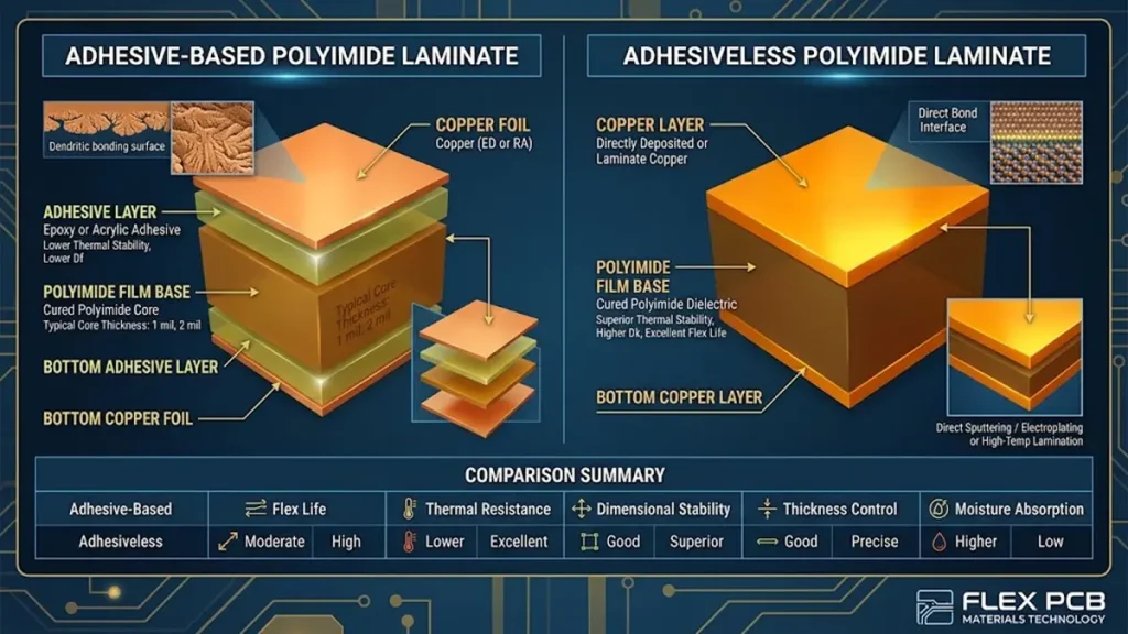
Comparison of Adhesive-Based vs. Adhesiveless Polyimide PCB Substrates
Polyimide substrates are not commodities. A roll of DuPont Pyralux AP adhesiveless laminate costs substantially more than generic PI film from regional suppliers, and the performance gap is measurable in thermal cycling and impedance stability. In 2026, brand-name adhesiveless polyimide runs between $10 and $25 per square foot, while adhesive-based alternatives sit closer to $6–$15 per square foot. For a 4-layer rigid-flex design, that delta alone can shift the unit price by 15–25%.
At Shenzhen Hongda Circuit, we maintain strategic inventory of DuPont, Arlon, and Shengyi polyimide cores. This allows us to offer tiered material options within the same RFQ response—giving procurement teams the data to decide whether a Class 3 aerospace build truly requires adhesiveless construction, or whether a standard adhesive-based stackup meets the reliability target at lower polyimide PCB fabrication cost.
Layer Count and Stackup Complexity
Every additional layer in a flexible or rigid-flex board introduces a lamination cycle, registration risk, and yield loss. Industry data shows that moving from 2-layer to 4-layer flex increases cost by 35–40%, and stepping up to 6-layer or 8-layer configurations escalates pricing even more steeply due to alignment challenges with dimensionally unstable polyimide films. At a per-step yield of 99.5% across 40 process steps, compound yield for complex multilayer flex drops to roughly 82%. Fabricators price that yield loss into every quotation.
Our recommendation: consolidate power and ground planes where possible, and avoid unnecessary blind or buried vias in the flexible sections. A simplified stackup not only reduces polyimide PCB cost—it also improves long-term bend reliability.
Copper Weight and Fine-Line Density
Standard 1 oz copper is the baseline for most flex applications. Moving to 2 oz copper increases etch time, material consumption, and scrap rates—typically adding 20–40% to processing costs. More importantly, heavy copper reduces dynamic flex life. For designs requiring high current, we advise localized copper plating rather than full-sheet heavy copper, preserving bend radius performance without the price penalty.
Fine-line traces below 3 mil (75 µm) width or spacing require Laser Direct Imaging (LDI) and advanced etch chemistry. These processes are standard at our facility but do carry a process-upcharge compared to conventional photolithography. If your design tolerances are tighter than 3/3 mil, expect the polyimide PCB price to reflect the imaging technology required.
Surface Finish Selection
Surface finish is one of the few cost levers procurement can adjust without affecting electrical performance—provided the choice matches the assembly environment. In descending order of cost:
- ENIG (Electroless Nickel Immersion Gold): $0.50–$2.00 per square inch. Best for fine-pitch and wire-bonding, but gold market volatility makes this the most expensive option.
- Immersion Silver: $0.15–$0.40 per square inch. Good solderability and flatness, shorter shelf life than ENIG.
- OSP (Organic Solderability Preservative): $0.05–$0.15 per square inch. Most economical, but limited to assemblies with short storage-to-reflow cycles.
For consumer electronics and industrial controls with standard assembly timelines, OSP or Immersion Silver can reduce polyimide PCB cost by 15–25% compared to ENIG without introducing solderability risk.
Testing, Certification, and Hidden Cost Drivers
Basic electrical testing (netlist flying probe) is standard. What inflates cost is the testing depth:
- 100% netlist testing vs. sampling: 5–10% price delta
- Impedance control with TDR reporting: 10–15% adder for stackup simulation and verification
- IPC Class 3, AS9100, or automotive IATF 16949 documentation: 5–8% management overhead per certification
Other hidden drivers include panel utilization efficiency—an L-shaped flex circuit can waste 40–50% of a standard 18″×24″ panel—and stiffener selection. PI stiffeners are thinner but cost more than FR-4; aluminum or copper stiffeners add both material and secondary-operation expense. Finally, expedited lead times (7-day turnaround vs. standard 14-day) typically carry a 20–30% premium.
How to Prepare a Bulletproof RFQ Package for Your Polyimide PCB Manufacturer
A delayed quote is almost always the result of incomplete documentation. When buyers ask, “How much does polyimide PCB cost?” the answer depends entirely on what you send. The following framework is what our engineering team at Shenzhen Hongda Circuit uses to evaluate incoming RFQs. Submit these items completely, and you will receive a firm quotation within 24 hours.
Essential Documentation Checklist
- Gerber Data (RS-274X or ODB++): Include all copper layers, solder mask, silkscreen, and board outline. The outline layer must be a closed polygon—missing board contours are the #1 reason quotes stall.
- Drill Files (Excellon Format): Clearly differentiate plated through-holes (PTH) from non-plated holes (NPTH). Include a drill table with finished sizes and tolerances.
- Stackup Drawing: Specify layer sequence, dielectric thicknesses, copper weights per layer, controlled-impedance targets, and Dk/Df values if known.
- Fabrication Drawing (PDF): Annotate overall dimensions, slot sizes, cutout locations, plating requirements, and surface finish.
- Material and Process Notes: State preferred polyimide brand/grade, coverlay color, stiffener type and placement, IPC class, and electrical test requirements.
- Commercial Terms: Quantities (prototype, pilot, annual forecast), target delivery date, and Incoterms.
DFM Pre-Submission Review
Before uploading files to our portal, run this 5-point check:
- Minimum trace/space: Confirm your design is within our stated capability (3 mil / 3 mil standard; 2 mil / 2 mil with LDI). If you have relaxed non-critical traces to 4 mil or wider, say so—etch yields improve, and cost drops.
- Annular ring and via pads: Ensure annular rings meet IPC-2223 flex-circuit requirements. Undersized rings in bend areas are a common DFM failure.
- Coverlay alignment: Verify that coverlay openings align with solder pads. Misalignment forces manual rework or scrap.
- Copper distribution balance: Asymmetric copper loading causes warpage during lamination. Balance pours across layers where possible.
- Bend radius compliance: IPC-2223 recommends a bend radius no tighter than 10× the total thickness of the flex region. Violations trigger engineering holds.
Common RFQ Mistakes That Delay Quotes
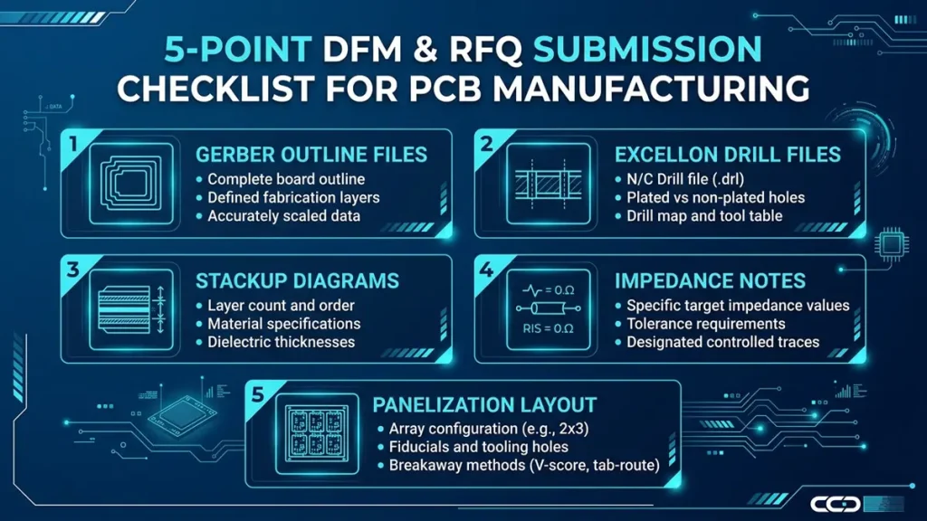
5-Point DFM & RFQ Submission Checklist for PCB Manufacturing
| Mistake | Consequence | Fix |
|---|---|---|
| Missing board outline layer | 2–3 day delay while engineering requests files | Verify GM1 or GKO layer is present and closed |
| No copper weight specified | Defaults to 1 oz; may not match power requirements | Annotate copper weight per layer in stackup or fab notes |
| Impedance control requested without network list | Forces full-board simulation, adding cost | List specific nets and target values |
| Vague test requirements | Defaults to sample test; may miss your quality gate | State “100% netlist + TDR report” explicitly |
| Ignoring panelization | Low nesting efficiency inflates unit cost | Ask your manufacturer to optimize panel layout before quoting |
Advanced Manufacturing Technology That Controls Polyimide PCB Fabrication Cost
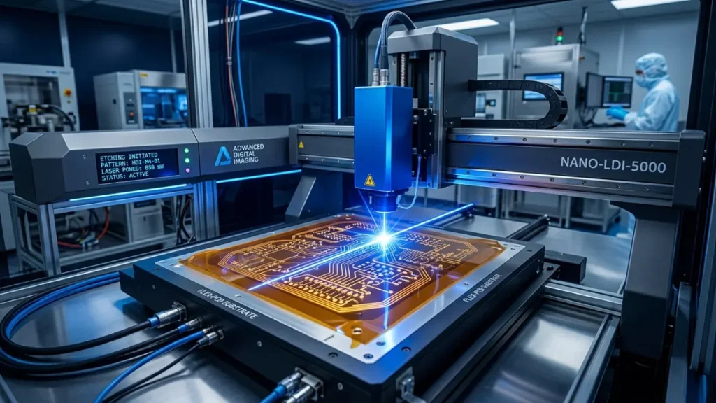
Laser Direct Imaging (LDI) Technology for High-Precision Polyimide Flex PCB Manufacturing
Cost is not only about what you specify—it is about how your flexible polyimide PCB supplier builds it. Older fabrication lines rely on phototools, manual alignment, and batch inspection. Modern lines use digital imaging, real-time process control, and automated optical inspection to drive yield up and scrap down. At Shenzhen Hongda Circuit, we have invested in the following capabilities specifically to contain polyimide PCB fabrication cost without cutting corners on quality.
Laser Direct Imaging (LDI) for Fine-Pitch Flex Circuits
Traditional photolithography uses a physical film and UV exposure. The film is susceptible to humidity distortion, scratches, and alignment drift—problems that multiply when polyimide substrates expand and contract between process steps. Laser Direct Imaging (LDI) eliminates the phototool entirely. A computer-controlled UV laser writes the circuit pattern directly onto photoresist, achieving line-width tolerances down to ±10% at 30 µm features.
For buyers, LDI translates to three cost advantages:
- No phototool NRE: Design revisions do not require new film sets.
- Real-time scaling: The software compensates for polyimide dimensional changes during processing, reducing layer-to-layer misalignment and subsequent scrap.
- Finer features on standard processes: You get HDI-level density without the HDI price premium.
Automated Optical Inspection (AOI) and Yield Recovery
Polyimide’s dimensional instability makes AOI calibration more complex than on rigid FR-4. Our lines use 3D AOI systems tuned for flexible substrates, detecting trace neck-downs, coverlay misregistration, and foreign material before boards reach electrical test. Catching defects at AOI—rather than after full lamination—prevents the compound cost of buried scrap in multilayer builds.
HDI and Microvia Technology for High-Density Designs
High-Density Interconnect (HDI) with laser-drilled microvias is no longer exclusive to rigid smartphone boards. In rigid-flex and multilayer flex applications, microvias reduce layer count by allowing routing density that would otherwise require 6 or 8 layers. A 4-layer HDI flex design can often replace a 6-layer through-hole flex design, cutting material, lamination, and test costs by 20–30%.
Shenzhen Hongda Circuit operates laser drilling platforms capable of 0.076 mm (3 mil) microvias in polyimide, with stacked-via structures for aerospace and medical applications. If your current polyimide PCB manufacturer cannot offer microvia-in-flex, you may be overpaying for unnecessary layer count.
Plasma Etching and Adhesiveless Lamination
Standard polyimide flex circuits use acrylic or epoxy adhesives to bond copper foil to the PI substrate. Adhesive layers add thickness, absorb moisture, and create a weak interface under thermal cycling. Adhesiveless lamination—where copper is cast or sputtered directly onto polyimide—eliminates this failure mode and reduces overall thickness by 20–30%.
The manufacturing challenge is that adhesiveless polyimide requires plasma desmear (plasma etching) for via cleaning, rather than conventional chemical desmear. We operate inline plasma systems that prepare microvia walls for plating without mechanical damage to the thin PI film. The result: higher reliability, thinner profiles, and long-term cost savings from reduced field failures.
Shenzhen Hongda’s Production Infrastructure
Founded in 1999, Shenzhen Hongda Circuit Technology Co., Ltd. has evolved from a conventional PCB shop into a high temperature polyimide PCB supplier with capabilities spanning 224 Gbps RF substrates, 120+ layer backplanes, and any-layer HDI. Our Bao’an district facility operates under ISO 9001, TS 16949, and AS9100 quality frameworks, with full RoHS and REACH compliance.
Key equipment relevant to polyimide and flex production includes:
- LDI direct imaging systems for sub-3 mil trace/space
- UV laser drills for microvias in flexible sections
- Precision hydraulic lamination presses with programmable pressure/temperature profiles for rigid-flex bonding
- Inline plasma treatment for adhesiveless PI surface activation
- 3D AOI and flying-probe test with impedance-controlled fixture verification
This infrastructure is not listed for marketing purposes. It is the reason we can quote complex rigid-flex builds with deterministic yield forecasts rather than speculative pricing.
Polyimide PCB Procurement Strategy: From Prototype to Volume Production
Volume Pricing Tiers and MOQ Optimization
Polyimide PCB cost per square inch drops dramatically with volume, but the curve is steeper than for rigid boards because setup and tooling represent a larger share of the total. Based on 2026 market data:
| PCB Type | Prototype (1–10 pcs) | Low Volume (100–500 pcs) | Mid Volume (1K–5K pcs) | High Volume (10K+ pcs) |
|---|---|---|---|---|
| Single-layer Flex | $150–$300 total | $3–$8/unit | $1.50–$4/unit | $0.50–$1.50/unit |
| 2-Layer Flex | $250–$500 total | $5–$15/unit | $3–$8/unit | $1–$3/unit |
| 4-Layer Flex | $400–$800 total | $15–$40/unit | $8–$20/unit | $3–$10/unit |
| Rigid-Flex (4L) | $600–$1,200 total | $25–$60/unit | $12–$30/unit | $5–$15/unit |
Note: Figures represent bare-board fabrication only, based on standard polyimide with OSP finish and 1 oz copper.
For buyers, the strategic implication is clear: consolidate prototype and pilot orders where possible. Ordering 5 pieces at a time triggers full setup charges repeatedly. A single 50-piece prototype lot amortizes tooling across more units and gives your engineering team spare boards for debugging.
Lead Time Management and Supply Chain Resilience
In 2026, raw material pricing pressure from gold, copper, and polyimide resin continues to compress quote validity windows. Lead times for specialty PI films can stretch to 4–6 weeks if a fabricator lacks inventory partnerships. At Shenzhen Hongda Circuit, we buffer strategic polyimide stock and maintain dual-source agreements with DuPont and domestic PI suppliers. For standard builds, this translates to prototype lead times of 5–7 days and production turns of 10–14 days, with expedite options available.
When evaluating where to buy polyimide PCB volumes, ask your supplier three questions:
- Do you hold polyimide raw stock, or do you order per job?
- What is your historical on-time delivery rate for flex and rigid-flex?
- Can you scale from 10 prototypes to 10,000 units without a factory transfer?
A supplier who hesitates on any of these points is introducing schedule risk into your program.
Why Buy Polyimide PCB from Shenzhen Hongda Circuit Technology
Certifications and Quality Framework
Not every polyimide PCB manufacturer carries the certifications required for regulated industries. Our quality system includes:
- ISO 9001:2015 — Foundation quality management
- IATF 16949 — Automotive production requirements
- AS9100D — Aerospace and defense quality standard
- IPC Class 3 — High-reliability product verification
- UL Recognition — Flammability and safety compliance
- RoHS / REACH — Environmental substance control
These certifications are not merely wall decorations. They dictate our process controls, incoming material inspection protocols, and traceability systems. For buyers in medical, automotive, and aerospace sectors, this documentation package is often mandatory for supplier qualification.
One-Stop RFQ Portal with Gerber Upload and 24-Hour Response
We have streamlined the polyimide PCB sourcing process into a single workflow:
- Upload your Gerber/ODB++ package through our secure RFQ portal at www.pcbkr.com.
- Auto-parse: Our system reads layer count, board dimensions, and drill counts to pre-populate the quote form.
- Specify parameters: Select polyimide grade, layer count, copper weight, surface finish, and test level from dropdown menus.
- Engineering review: Within 15 minutes, our DFM engine flags potential manufacturing issues. Within 24 hours, a human engineer sends a firm quote with itemized cost breakdown.
- Iterate online: Modify quantities or materials and regenerate quotes without re-uploading files.
For buyers managing multiple programs, this eliminates the email-thread chaos of traditional RFQ management. You retain a complete audit trail of specifications, revisions, and pricing history.
Frequently Asked Questions: Polyimide PCB Manufacturer Selection
How do I verify a polyimide PCB manufacturer’s actual capabilities before placing an order?
Request a process capability document (PCD) specific to flexible and rigid-flex products. Verify minimum trace/space, smallest mechanical drill, laser microvia capability, and maximum layer count for flex builds. Ask for a factory tour or virtual audit focusing on lamination, imaging, and test areas. At Shenzhen Hongda Circuit, we provide capability matrices backed by equipment calibration records and IPC qualification test data.
What is the realistic polyimide PCB cost per square inch for prototypes vs. volume production?
For standard 2-layer polyimide flex with OSP finish, expect $1.80–$3.50 per square inch at prototype volumes (1–10 pieces), dropping to $0.30–$0.80 per square inch at 10,000+ piece volumes. Rigid-flex and multilayer configurations scale higher. The key variable is panel utilization—optimizing your board outline to nest efficiently on an 18″×24″ panel can reduce unit cost by 20% without changing a single electrical parameter.
How can I reduce polyimide PCB fabrication cost without sacrificing reliability?
Five proven polyimide PCB cost reduction strategies: (1) Use standard PI thicknesses (25 µm or 50 µm) to leverage volume material pricing. (2) Minimize layer count by consolidating planes and using HDI microvias where appropriate. (3) Select OSP or Immersion Silver instead of ENIG for non-critical assemblies. (4) Optimize panel layout with your manufacturer before finalizing the board outline. (5) Provide complete RFQ documentation on the first submission to avoid engineering-review delays that compress lead times and trigger expedite fees.
What certifications should a qualified polyimide PCB supplier hold for aerospace and automotive?
For aerospace, AS9100D and IPC Class 3 are baseline requirements; NADCAP accreditation for special processes (plating, chemical processing) is a strong differentiator. For automotive, IATF 16949 is mandatory, with PPAP Level 3 submission capability for production parts. Medical devices typically require ISO 13485. Always verify that the supplier’s certification scope explicitly includes flexible and rigid-flex PCB manufacturing—not just rigid boards.
How do I prepare Gerber files and stackup documents to get an accurate polyimide PCB quote in 24 hours?
Follow the polyimide PCB RFQ file requirements checklist: (1) RS-274X Gerbers with a closed board-outline layer. (2) Excellon drill file with PTH/NPTH distinction. (3) PDF fabrication drawing with dimensions, tolerances, and surface finish callouts. (4) Stackup table showing layer sequence, dielectric thicknesses, copper weights, and impedance targets. (5) Text readme file specifying material brand preference, IPC class, test coverage, and quantity/lead-time needs. Submitting all five items together is the single biggest factor in receiving a same-day firm quote.
Conclusion: Make Your Next Polyimide PCB Purchase Data-Driven
Polyimide PCB procurement does not have to be a black box. By understanding the six core cost drivers—material, layer count, copper weight, surface finish, testing, and hidden overhead—you can have an informed conversation with any polyimide PCB manufacturer. By preparing complete RFQ documentation and leveraging DFM feedback early, you eliminate the delays and surprise upcharges that derail product launches.
At Shenzhen Hongda Circuit Technology Co., Ltd., we combine advanced manufacturing infrastructure with a transparent quoting process designed for buyers who need both speed and certainty. Whether you are sourcing a 2-layer flex prototype for a wearable device or a 12-layer rigid-flex assembly for an aerospace controller, our engineering team is available to review your design and provide a detailed cost breakdown within 24 hours.
Ready to move forward? Upload your Gerber package to www.pcbkr.com and receive a firm polyimide PCB quote with DFM optimization recommendations—no obligation, no hidden fees.
Shenzhen Hongda Circuit Technology Co., Ltd. (PCBKR) — High-precision PCB & PCBA manufacturing since 1999. ISO 9001 | IATF 16949 | AS9100D | IPC Class 3.
About Author
David Chen https://www.linkedin.com/in/pcbcoming
David Chen boasts an extensive professional background in PCBA manufacturing, PCBA testing, and PCBA optimization, with specialized expertise in high-precision PCBA fault analysis and rigorous PCBA reliability testing. The author has worked with high-layer-count server PCB fabrication, ultra-low-loss backplane stackups, and thermo-mechanical reliability optimization for AI infrastructure projects involving 112G and 224G PAM4 architectures. Skilled in complex circuit design and cutting-edge advanced PCB manufacturing processes, he delivers solutions that elevate product durability and performance across industrial applications. His technical articles focusing on PCBA manufacturing workflows and testing methodologies are widely cited by industry peers, research institutions, and technical platforms, solidifying his reputation as a recognized technical authority in the global circuit board manufacturing sector.