PCB and PCBA New Product Introduction (NPI) Engineering: DFM, Verification, and Production Readiness
During NPI, our engineering team reviews your PCB design, stackup, BOM, and test plan against real manufacturing limits before tooling is cut. At Shenzhen Hongda Circuit Technology, this means DFM/DFA/DFT checks, impedance and via verification, component qualification, and a documented ECO process — turning a working prototype into a repeatable, yield-stable production build.
What Is NPI Engineering in PCB and PCBA Manufacturing?
NPI (New Product Introduction) engineering is the structured review stage between “the design works” and “the design is manufacturable at volume” — it converts a customer’s Gerber/ODB++ package and BOM into a validated production file set with documented tolerances, test coverage, and risk sign-off.
Most fabless teams underestimate how much changes between a 5-piece prototype run and a 5,000-piece SMT lot. A prototype panel can be hand-placed, hand-soldered, and visually inspected board-by-board. A production panel runs on a stencil printer at 150+ boards/hour, a reflow oven with a fixed thermal profile, and an AOI system with a fixed pass/fail threshold. NPI engineering is the gate that catches the difference before the customer pays for a full production lot that doesn’t reflow cleanly or route correctly through pick-and-place.
At our facility, every new job number over 50 pieces or containing BGA/QFN packages under 0.5mm pitch is automatically routed through a five-stage NPI checklist — design review, stackup/impedance verification, DFM, DFA/DFT, and BOM qualification — before it is released to the floor.
What Happens During PCB Design and Stackup Review Before Tooling?
Our engineers cross-check the layer stackup against your target impedance, verify dielectric thickness and copper weight per layer, and confirm trace/space and annular ring values sit inside our process window — typically 3.5/3.5mil minimum trace/space for standard 1-6 layer boards and 3/3mil for HDI, with impedance held to ±10% (or ±7% on request for RF/high-speed designs).
Manufacturing pain point: The single most common stackup failure we see from new customers is a dielectric constant (Dk) mismatch between the design file’s assumed Dk and the actual laminate lot’s Dk, which shifts controlled-impedance traces by 8–15% — enough to fail a 50Ω ±10% spec on a USB 3.0 or DDR4 board. We run a Time Domain Reflectometry (TDR) coupon on every impedance-controlled panel, not a sample panel, because Dk can drift lot-to-lot even from the same laminate supplier (typical FR-4 Dk variance: 4.2–4.8 at 1GHz).
Scenario: A customer submitted a 6-layer, 1.6mm board with a 100Ω differential pair for a USB 3.0 interface, designed assuming Dk = 4.3. Our incoming laminate lot measured Dk = 4.55. Left uncorrected, the pair would have measured ~108Ω — a fail. Our stackup engineer adjusted trace width from 5mil to 4.7mil and re-ran the field-solver model before the panel was released, holding the pair at 99.2Ω measured on the TDR coupon.
What Does DFM (Design for Manufacturability) Analysis Actually Check?

NPI Engineering DFM Analysis and Multi-Layer PCB Design
DFM checks whether the copper artwork, drill file, and solder mask geometry can physically survive our fabrication process — minimum hole size vs. board thickness (aspect ratio), copper-to-edge clearance, solder mask dam width, and panelization fit — flagged against IPC-2221/IPC-6012 Class 2 or Class 3 limits depending on the end-use.
Manufacturing pain point: Aspect ratio violations are the leading cause of NPI hold-ups on multilayer boards. A 0.2mm (8mil) drilled hole in a 3.2mm-thick, 12-layer backplane gives a 16:1 aspect ratio — well past our reliable plating limit of 10:1 for through-holes. Beyond 10:1, copper plating thickness at the hole barrel midpoint drops below the 20µm (0.8mil) minimum required by IPC-6012 Class 2, risking barrel cracking under thermal cycling.
Other DFM flags we run on every job: annular ring below 0.075mm (3mil), solder mask dam under 0.1mm between fine-pitch pads, copper-to-board-edge under 0.3mm (routing risk), and negative/positive artwork mismatches on inner layers.
What Is DFA and How Does It Prevent Assembly-Stage Failures?

NPI Engineering SMT Assembly and DFA Verification
DFA (Design for Assembly) verifies that component footprints, land patterns, and component-to-component spacing are compatible with our SMT line’s placement accuracy and reflow profile — catching problems like tombstoning risk, insufficient thermal relief on ground pads, and components placed too close to the board edge for our pick-and-place nozzle clearance.
Manufacturing pain point: Tombstoning on 0201 and 01005 passives is almost always a DFA issue, not a process issue — it happens when pad copper area is asymmetric (one pad connected to a large ground plane without thermal relief pulls heat away faster during reflow, causing the component to lift on the cooler side). We require a minimum thermal relief spoke width of 0.3mm on any 0201/01005 pad tied directly to a plane layer.
Scenario: On a motor-driver PCBA with 180 × 01005 decoupling capacitors, an early design had 12% of those pads tied directly to a solid ground pour with no thermal relief. First-article SMT run showed 9 tombstoned parts (5% defect rate on that population). Adding thermal relief spokes and re-running the reflow profile brought the defect rate to zero on the next 500-unit lot.
What Does DFT (Design for Testability) Cover, and How Are Test Points Planned?
DFT confirms every net that needs in-circuit or functional verification has an accessible test point — minimum 0.9mm (35mil) pad diameter on a 2.54mm or 1.27mm grid for bed-of-nails ICT, or defined boundary-scan (JTAG) coverage for BGA nets with no physical test access.
Manufacturing pain point: Boards with high BGA density often have 15–30% of nets with zero physical test access once the board is populated. Without DFT planning at the NPI stage, this shows up as “untestable” nets discovered only after the first PCBA build, forcing a re-spin. We map test coverage against the schematic net list before tooling and flag any net below 100% test access for either an added test point or a documented functional-test workaround.
How Is the BOM Reviewed and Are Components Qualified for Production?
BOM review cross-checks every line item for lifecycle status (active vs. NRND/EOL), verifies footprint-to-datasheet match, confirms RoHS/REACH compliance documentation, and flags single-source or long-lead components (currently 16–52 weeks for certain MLCC and MOSFET part numbers) before the order is placed.
Manufacturing pain point: The most expensive BOM error we catch is a footprint mismatch that isn’t visible until placement — for example, a BOM listing a 0.5mm-pitch QFN-32 while the PCB land pattern was laid out for a 0.4mm-pitch variant of the “same” part number from a different manufacturer. This passes visual BOM review but fails at first-article placement, scrapping the panel. Our component engineer verifies pin-1 orientation, thermal pad size, and pitch against the actual manufacturer datasheet — not just the part number — for every BGA/QFN line item.
How Are Via and Through-Hole Structures Verified for Long-Term Reliability?
We verify via type (through-hole, blind, buried, or via-in-pad), plating thickness, and aspect ratio against board thickness, and confirm via-in-pad structures are filled and capped per IPC-4761 Type VII when used under BGA pads, since an unfilled via under a BGA ball can wick solder away from the joint during reflow.
Manufacturing pain point: Via-in-pad without proper copper fill is a silent failure mode — the board passes electrical test and even initial reflow, but solder wicks into the via cavity over repeated thermal cycling (common in automotive and industrial applications with -40°C to +125°C cycling), thinning the solder joint until it fails in the field months later. We require conductive or non-conductive epoxy fill with copper cap plating on any via-in-pad under a fine-pitch BGA, verified by cross-section sampling on the first article.
What SMT Placement and Reflow Checks Happen Before Mass Production?
Before releasing a job to full production, we run a first-article SMT build validating stencil aperture-to-pad ratio (target 0.66–0.75 area ratio for fine-pitch parts), placement accuracy (±0.05mm on our current pick-and-place equipment), and a reflow profile matched to the specific paste alloy — typically a peak of 245–250°C for SAC305 lead-free solder with a time-above-liquidus of 45–75 seconds.
Manufacturing pain point: BGA voiding above 25% (measured by X-ray, per IPC-A-610 Class 2 acceptance) is most often a stencil aperture or paste-volume issue, not a placement issue — insufficient paste volume under the BGA ball traps outgassing flux that can’t escape before the joint solidifies. We adjust stencil thickness (typically 0.1–0.15mm) and aperture design specifically for BGA voiding control, then confirm with X-ray on the first-article sample before authorizing the full lot.
How Are Engineering Change Orders (ECOs) Managed During NPI?
NPI Engineering ECO Management Process and Version Control
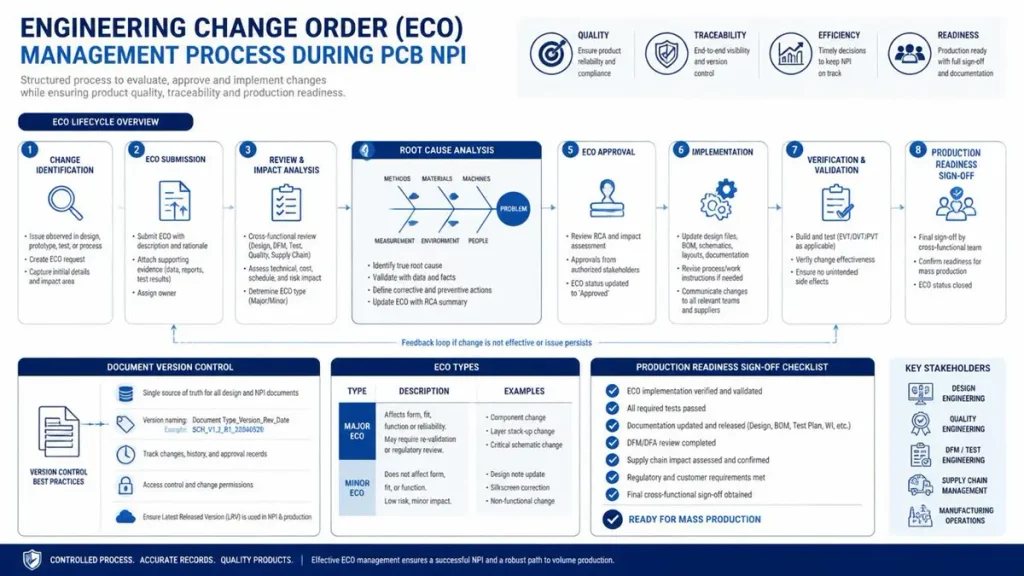
Every change discovered during design review, DFM, or first-article build is logged as a formal ECO with revision number, root cause, and affected documentation (Gerbers, BOM, pick-and-place file, test plan) — the panel is not released to full production until every open ECO on that revision is closed and re-verified.
This documentation trail matters most when a defect surfaces months later: with a closed-loop ECO record, we can trace exactly which board revision, stencil, and reflow profile produced any given lot — critical for automotive (IATF 16949) and medical customers where full traceability is a contractual requirement, not a convenience.
How Does Prototype Feedback Confirm the Design Is Ready for Production?
We run first-article inspection (AOI + X-ray + electrical test) on the initial pilot lot — typically 20–50 units — and feed measured data (impedance, hole registration, solder joint quality, functional test yield) back to the customer before committing to full-volume tooling and purchasing long-lead components.
Manufacturing pain point: Skipping pilot-lot feedback to save 3–5 days is the single most common cause of scrapped production runs we see — a customer under schedule pressure authorizes full volume straight after a 5-piece hand-built prototype, and a process-related defect that only appears at machine-placement scale (tombstoning, voiding, or a marginal test point) shows up across the entire lot instead of a 20-unit pilot.
How Does NPI Engineering Differ From Our Overall NPI PCB Service?
Our broader NPI PCB service covers the entire path from quote to volume shipment — sourcing, fabrication, assembly, and logistics. This page covers specifically what our engineering team does inside that process: the design review, DFM/DFA/DFT analysis, and sign-off work that happens before a single panel is drilled or placed.
FAQs: What Procurement Buyers Search Before Choosing a PCB/PCBA Supplier
What is NPI in PCB manufacturing, and why does it matter when choosing a supplier?
NPI (New Product Introduction) is the engineering review stage between prototype and volume production. A supplier with a documented NPI process catches design-to-manufacturing mismatches (impedance, DFM, DFA, DFT) before you pay for a full production lot, reducing the risk of a costly re-spin.
How long does NPI engineering typically add to the production timeline?
For a standard 4–8 layer board, DFM/DFA/DFT review and stackup verification typically add 1–3 business days before tooling; for HDI or impedance-critical designs (RF, high-speed digital), allow 3–5 business days to include TDR coupon verification and a pilot-lot build.
Is DFM/DFA review included in the quote, or billed separately?
Reputable manufacturers include a baseline DFM check in every quote at no extra charge. Deeper services — TDR impedance verification, X-ray voiding analysis, or a documented pilot-lot report — are sometimes itemized separately; ask your supplier to specify what’s included before comparing quotes.
What files and information should I provide to get an accurate NPI engineering review?
At minimum: Gerber/ODB++ files, drill file, IPC netlist, a complete BOM with manufacturer part numbers (not generic descriptions), assembly drawing, and your target end-use environment (consumer, industrial, automotive, or medical) so the reviewer applies the correct IPC class and test coverage.
What certifications or standards should a supplier’s NPI engineering team reference?
Look for explicit reference to IPC-2221 (design standards), IPC-6012 (fabrication acceptance, Class 2/3), IPC-A-610 (assembly acceptance), and IPC-4761 (via protection) in their process documentation — and, for automotive or medical work, IATF 16949 or ISO 13485 traceability.
About Author
David Chen https://www.linkedin.com/in/pcbcoming
David Chen is a Senior RF/PCB Process Engineer at Shenzhen Hongda Circuit Technology Co., Ltd., with over 12 years of experience in high-frequency PCB fabrication, impedance-controlled stack-up design, and Rogers/PTFE laminate processing. He also boasts an extensive professional background in PCBA manufacturing, PCBA testing, and PCBA optimization, with specialized expertise in high-precision PCBA fault analysis and rigorous PCBA reliability testing. The author has worked with high-layer-count server PCB fabrication, ultra-low-loss backplane stackups, and thermo-mechanical reliability optimization for AI infrastructure projects involving 112G and 224G PAM4 architectures. Skilled in complex circuit design and cutting-edge advanced PCB manufacturing processes, he delivers solutions that elevate product durability and performance across industrial applications. His technical articles focusing on PCBA manufacturing workflows and testing methodologies are widely cited by industry peers and technical platforms, and have gained attention and recognition from industry colleagues.