
How Do You Choose a Bluetooth Module PCB Manufacturer for Reliable RF Performance?
A reliable Bluetooth Module PCB manufacturer must control PCB geometry, RF impedance, antenna clearance, grounding, soldering quality, and production repeatability—not just fabricate the Gerber files. For Bluetooth products operating in the 2.4 GHz band, buyers should evaluate the module reference design, PCB stackup, RF-feed structure, assembly controls, and verification plan together before approving prototypes or mass production.
Table of Contents
- What Is a Bluetooth Module PCB, and Which Manufacturing Route Should You Choose?
- Which PCB Stackup and Materials Are Suitable for Bluetooth Modules?
- How Should a Bluetooth Module PCB Handle Antenna Clearance and 50-Ohm RF Routing?
- Which Advanced PCB Manufacturing Technologies Improve Bluetooth Module PCB Consistency?
- What Manufacturing Problems Commonly Cause Bluetooth PCB Failures?
- How Should Bluetooth Module PCB DFM and Assembly Be Reviewed Before Production?
- How Can Buyers Verify Bluetooth PCB Quality and RF Performance?
- What Determines Bluetooth Module PCB Manufacturing Cost and Lead Time?
- How Do You Select a Bluetooth Module PCB Manufacturer for Volume Production?
- What Should a Bluetooth Module PCB RFQ Include?
- What Should Buyers Ask a Bluetooth Module PCB Supplier Before Ordering?
What Is a Bluetooth Module PCB, and Which Manufacturing Route Should You Choose?
A Bluetooth Module PCB is a printed circuit board that hosts a Bluetooth radio module or Bluetooth-related circuitry and connects it to the product’s power, control, sensor, and communication interfaces. The right manufacturing route depends on whether the design uses a pre-certified module, a separate antenna, or a custom Bluetooth RF circuit.
Bluetooth-enabled products include industrial sensors, handheld instruments, medical and laboratory equipment, smart locks, control panels, wearable devices, wireless data loggers, and IoT gateways. Although these products share the Bluetooth name, their PCB requirements can differ substantially.
Should you use a pre-certified Bluetooth module or a custom RF design?
A pre-certified module can reduce RF design effort, but it does not eliminate host-board layout requirements or automatically certify the complete end product. Buyers still need to follow the module manufacturer’s antenna, grounding, power-supply, and placement instructions.
| Design route | PCB manufacturing considerations | Main procurement risk |
|---|---|---|
| Module with integrated antenna | Host-board copper clearance, module placement, ground-plane geometry | Antenna detuning caused by the host PCB or enclosure |
| Module with external antenna connector | Controlled-impedance RF feed, connector footprint, matching components | RF loss or impedance discontinuity between module and antenna |
| Bluetooth SoC with a custom RF circuit | RF layout, matching network, reference design, clock and power integrity | Greater development, tuning, and verification workload |
| Bluetooth module on a compact sensor board | Board outline, component density, power noise, mechanical integration | Reduced antenna performance after enclosure assembly |
Engineering decision: Confirm the exact module part number and hardware-design revision before requesting a quote. A manufacturer cannot accurately review antenna clearance, RF trace geometry, or module footprint details using only a generic description such as “Bluetooth 5.x PCB.”
For a buyer sourcing both bare boards and assembly, the RFQ should identify whether the required deliverable is bare PCB fabrication, PCBA, or turnkey procurement and assembly.
Which PCB Stackup and Materials Are Suitable for Bluetooth Modules?
Standard FR-4 is suitable for many Bluetooth module host boards, including many designs with a 2.4 GHz RF feed, provided the selected laminate, dielectric thickness, copper geometry, and ground reference support the required impedance. Two-layer and four-layer constructions are both viable; the correct choice depends on routing density, noise control, antenna design, and the module manufacturer’s reference layout.
A four-layer PCB often makes it easier to maintain a continuous ground reference and separate noisy digital or power routing from sensitive RF sections. It is not automatically necessary for every Bluetooth product, and extra layers do not compensate for an incorrect antenna keepout.
How should buyers compare two-layer and four-layer Bluetooth PCBs?
| Design factor | Two-layer PCB | Four-layer PCB |
|---|---|---|
| Cost and construction | Often lower cost and simpler | Higher material and process cost in many designs |
| Ground reference | Requires careful bottom-layer routing and ground continuity | Can provide a dedicated internal ground plane |
| Routing density | Suitable for simpler layouts | More routing flexibility for compact, complex products |
| Noise isolation | More dependent on placement and routing discipline | Can improve return-path control when correctly designed |
| RF-feed design | 50 Ω geometry must be calculated for the actual structure | 50 Ω geometry must be calculated for the actual structure |
| Best fit | Simple modules, basic controllers, cost-sensitive products | Dense sensor boards, mixed digital/RF designs, compact products with more interfaces |
Which stackup parameters must be agreed before fabrication?
The manufacturer should review the following items before releasing the production stackup:
- Finished board thickness and tolerance.
- Copper weight on each layer.
- Dielectric thickness between the RF trace and its reference plane.
- Laminate dielectric properties used for impedance calculation.
- Solder mask over or around the RF feed, where relevant to the impedance model.
- Copper spacing and ground-via arrangement for coplanar structures.
- Finished copper and trace geometry after etching.
- Whether impedance coupons and a controlled-impedance test report are required.
A nominal 50 Ω target does not determine trace width by itself. Trace width and gap depend on the complete geometry, including dielectric height, material properties, copper thickness, and the selected transmission-line structure. A width copied from another design can be wrong even if both boards use “FR-4.”
Scenario: a compact industrial sensor. The original design may fit a two-layer board, but adding a display, switching regulator, connector, and sensor interface can force digital signals close to the RF feed. A four-layer stackup may improve routing and return-path control, but the antenna clearance and reference design must still be preserved.
For procurement, request a proposed stackup and impedance calculation before approving a quotation that assumes a generic FR-4 construction.
How Should a Bluetooth Module PCB Handle Antenna Clearance and 50-Ohm RF Routing?
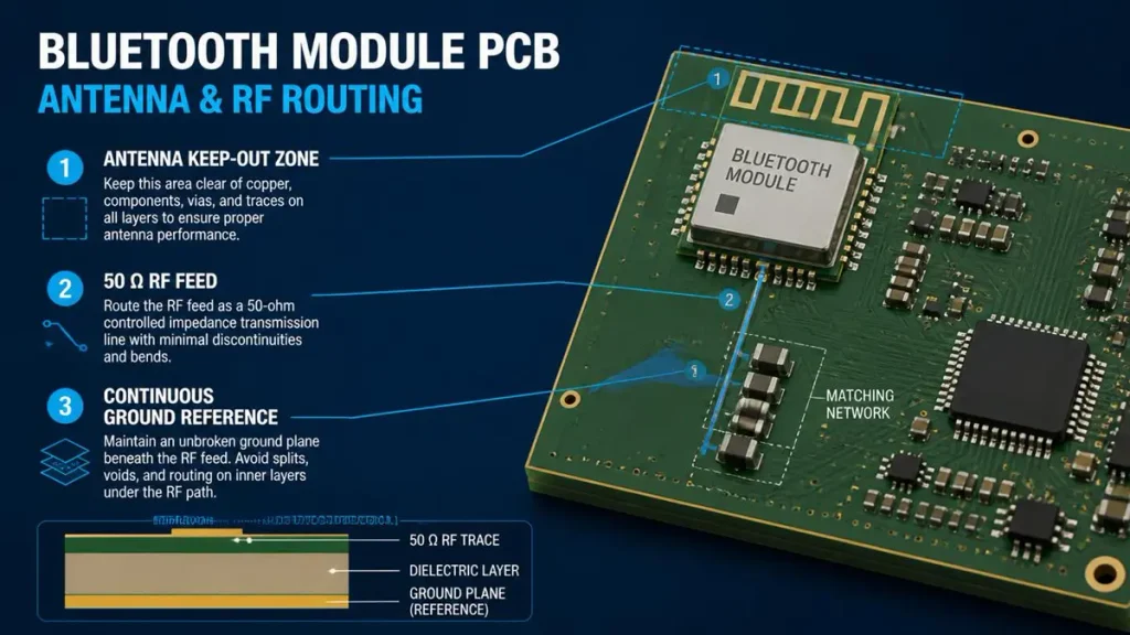
Bluetooth Module PCB antenna clearance, 50-ohm RF routing, and continuous ground reference
Follow the antenna and module manufacturer’s exact placement and keepout drawings, maintain the specified RF transmission-line impedance—commonly 50 Ω for a single-ended RF feed—and preserve a continuous reference ground along the feed. Antenna clearance is design-specific; there is no single universal keepout distance suitable for every Bluetooth module or antenna.
Bluetooth commonly operates in the 2.4 GHz ISM band. At these frequencies, nearby copper, metalwork, batteries, cables, display frames, and even a changed ground-plane boundary can alter antenna behavior. The PCB layout must therefore be assessed together with the mechanical enclosure.
What should the manufacturer check around the antenna?
- Keepout on every relevant layer: Follow the module’s reference design for copper, traces, components, vias, and planes. A top-layer clearance alone may be insufficient.
- Board-edge placement: Where required by the reference design, position the antenna near the board edge and orient it toward the intended non-metallic region of the enclosure.
- Metal and battery proximity: Check brackets, shields, batteries, display frames, screws, cables, and nearby boards against the module’s specified clearance.
- Ground continuity: Avoid routing the RF feed across a split or interrupted reference plane.
- Matching-network placement: Preserve the reference circuit and component locations unless the RF design is deliberately revalidated.
- Enclosure-level verification: Evaluate RF behavior in the final mechanical configuration, not only on an open bench.
Manufacturer guidance from Infineon and Microchip specifically warns that antenna keepout requirements depend on the antenna and can apply to copper on multiple PCB layers. Follow the selected module’s own documentation rather than adopting a generic clearance figure. Infineon hardware design guidance and Microchip module placement guidelines.
How should a 50 Ω RF feed be manufactured?
The RF feed should be designed using the actual stackup and the chosen microstrip or grounded coplanar waveguide geometry. A manufacturer should not change the trace width, ground gap, copper weight, or dielectric thickness without evaluating the impedance consequences.
The manufacturing review should confirm:
- The RF trace and ground geometry match the approved fabrication data.
- The reference ground is continuous along the intended RF route.
- Vias, bends, connectors, and component pads do not introduce unreviewed discontinuities.
- Any impedance-controlled requirement is clearly identified on the fabrication drawing.
- The impedance coupon structure and test method are agreed before production.
- RF matching components are assembled in the correct positions and orientations.
A nominal 50 Ω design target is not the same as a verified 50 Ω production result. If controlled impedance is required, specify the tolerance and reporting requirements in the RFQ and confirm them against the actual stackup.
Scenario: the prototype passes on the bench but fails after enclosure assembly. The root cause may be a battery or metal bracket near the antenna, a shifted antenna position, a changed plastic-wall thickness, or an unintended copper area beneath the antenna. Reordering the same PCB without reviewing the mechanical environment may reproduce the failure.
Which Advanced PCB Manufacturing Technologies Improve Bluetooth Module PCB Consistency?
Advanced imaging, controlled lamination, precision drilling, fine-line patterning, automated inspection, and electrical testing can improve PCB geometry and repeatability. Their value for a Bluetooth module depends on the design’s actual tolerances: a conventional module board may not need ultra-fine mSAP features, while a compact, dense RF-and-digital design may benefit from tighter imaging and registration control.
PCBKR’s available equipment and process information includes SCREEN Ledia laser direct imaging (LDI), LAUFFER lamination equipment, Mitsubishi UV/CO₂ laser drilling, and picosecond laser processing. These are manufacturing-process capabilities, not automatic guarantees of a Bluetooth board’s RF performance. The approved stackup, production drawing, process qualification, and test results remain the acceptance basis.
How does advanced imaging help Bluetooth PCB production?
Laser direct imaging transfers the circuit pattern without relying on conventional phototool alignment in the same way as traditional exposure workflows. PCBKR’s supplied equipment data lists SCREEN Ledia LDI with 8 µm imaging capability and ±10 µm positioning accuracy under the stated process conditions.
For a typical Bluetooth host board, the most important benefit may be consistent reproduction of the RF trace, ground gap, fine-pitch module pads, and solder-mask openings—not the ability to manufacture the smallest possible line and space.
Manufacturing pain point: If a trace becomes narrower or the coplanar ground gap changes during imaging and etching, the transmission-line geometry may shift from the approved design. Whether this affects the finished impedance depends on the complete stackup and process variation, so the correct control is an agreed geometry and verification plan rather than an unsupported claim that finer imaging alone ensures better RF.
When does mSAP or fine-line processing matter?
Modified semi-additive processing (mSAP) can support fine-line circuit patterns in dense designs. PCBKR’s supplied process information lists 8/8 µm mSAP capability introduced in Q3 2024. This capability is relevant where component escape routing, dense fanout, or miniaturization requires features beyond conventional subtractive etching.
However, 8/8 µm mSAP is not a default requirement for Bluetooth PCBs. It should be specified only when the board design requires it and the complete process has been reviewed. For many module-based designs, correct antenna geometry, ground continuity, solderability, and assembly quality have greater practical impact than minimum line/space capability. For compact Bluetooth products with fine-pitch components and dense routing requirements, HDI PCB manufacturing may provide additional routing flexibility, depending on the required layer structure, via design, and component density.
How do precision drilling and lamination affect multilayer boards?
PCBKR’s supplied equipment data lists Mitsubishi UV/CO₂ laser drilling with a 75 µm drilling capability and ±5 µm tolerance, as well as picosecond laser processing for 50 µm features. Actual achievable via dimensions depend on the material system, aspect ratio, copper treatment, plating process, and product design.
LAUFFER lamination equipment data includes pressure settings of 80, 150, and 200 psi and vacuum below 50 mbar. These settings describe equipment capability, not a universal recipe for Bluetooth PCBs. The correct pressure, temperature, vacuum, and cycle must be selected for the laminate, resin system, copper distribution, and stackup.
For a four-layer Bluetooth board, stable lamination helps maintain the intended dielectric structure and layer registration. Those dimensions contribute to the impedance model, but RF acceptance still depends on the finished board and agreed test criteria.
Which inspection technologies are useful for Bluetooth module PCBA?
| Process or tool | What it can verify | What it cannot prove by itself |
|---|---|---|
| LDI and process dimensional checks | Pattern transfer and selected geometric features | Finished RF performance |
| Automated optical inspection (AOI) | Visible pattern defects, opens, shorts, selected assembly defects | Hidden solder joints or antenna tuning |
| X-ray inspection | Hidden solder-joint features, such as selected BGA or shielded joints | RF range or OTA performance |
| Electrical continuity/isolation testing | Specified net connectivity and isolation | 50 Ω impedance or antenna efficiency |
| Controlled-impedance testing | Impedance of the defined test structure using the agreed method | Complete product RF performance |
| RF or over-the-air (OTA) testing | Specified RF behavior under the defined test setup | Unspecified operating environments or all regulatory requirements |
Procurement recommendation: Ask the supplier which process capability applies to your board, what tolerance is being guaranteed, and what report will be supplied. A machine specification should never be substituted for a finished-product acceptance criterion.
What Manufacturing Problems Commonly Cause Bluetooth PCB Failures?
Common failure sources include antenna keepout violations, incorrect RF geometry, discontinuous ground, noisy power routing, component substitutions, soldering defects, and changes to the enclosure or stackup after validation. Many failures occur at the interface between electrical design, PCB fabrication, PCBA, and mechanical integration rather than in the Bluetooth module alone.
The following table maps typical symptoms to likely manufacturing or design causes and practical controls.
| Observed symptom | Potential cause to investigate | Recommended control |
|---|---|---|
| Shorter wireless range after assembly | Antenna detuning by copper, metal, battery, or enclosure | Review antenna keepout and test in final enclosure |
| Intermittent connection near a motor or switching regulator | Conducted or radiated noise, poor grounding, supply ripple | Review power layout, filtering, ground return, and system-level EMC |
| RF behavior differs between PCB lots | Stackup or geometry variation, changed materials, unapproved process changes | Freeze stackup, material construction, impedance criteria, and change control |
| RF performance changes after component replacement | Different parasitics or package geometry in matching components | Control manufacturer part numbers, package sizes, and approved substitutions |
| Module pads show solder defects | Footprint mismatch, paste design, warpage, stencil or reflow issues | Review land pattern, assembly drawing, stencil, and reflow profile |
| Bare-board electrical test passes but product fails RF test | Electrical connectivity does not establish RF performance | Add defined RF/functional verification and enclosure-level checks |
Why can a PCB pass electrical testing but fail Bluetooth performance?
A standard electrical test typically checks specified connectivity and isolation. It does not establish antenna efficiency, radiated output, receiver sensitivity, or reliable operation in the final enclosure. Similarly, AOI can detect many visible assembly defects but cannot confirm RF tuning.
Engineering troubleshooting sequence: When range or connection stability deteriorates, first compare the failing assembly with the approved reference design. Check the antenna clearance, ground-plane shape, stackup, RF-feed geometry, matching-component values, supply decoupling, and mechanical surroundings. Then isolate the fault through controlled RF measurements rather than immediately changing trace widths or replacing components.
This sequence is useful because an unplanned “fix” to the antenna or ground plane may improve one sample while making production less repeatable.
What should happen when a Bluetooth PCB revision changes?
Treat changes to laminate construction, dielectric thickness, copper weight, RF trace geometry, antenna position, matching components, shield, or enclosure as potential RF-impacting changes. Review the impact before release and define which tests must be repeated.
The change record should identify the affected drawing or BOM revision, reason for the change, approval owner, and required validation. This prevents an apparently minor cost-saving substitution from invalidating the reference design or the test results.
How Should Bluetooth Module PCB DFM and Assembly Be Reviewed Before Production?
A Bluetooth PCB DFM review should check the fabrication files, stackup, RF geometry, antenna keepout, module footprint, component package, solder-mask and copper clearances, panelization, and test access before production begins. The goal is to identify issues while the design is still inexpensive to change.
Which files should buyers send for a useful DFM review?
At minimum, prepare the Gerber or IPC-2581 fabrication data, drill files, stackup requirements, board thickness, copper weights, controlled-impedance notes, assembly drawings, BOM, pick-and-place data, and the exact Bluetooth module reference design.
Include the enclosure drawing or a mechanical keepout drawing when the antenna interacts with a battery, metalwork, shield, or plastic housing. If the design includes an external antenna connector, provide the connector specification and intended RF test arrangement.
Which DFM checks should be completed before the first prototype?
| Review item | What the manufacturer should confirm | Risk if omitted |
|---|---|---|
| Fabrication data | Layer count, drill data, outline, copper layers, revision consistency | Incorrect build or quotation assumptions |
| Stackup | Finished thickness, dielectric construction, copper weight | Incorrect impedance or mechanical fit |
| RF route | Target impedance, reference plane, line/gap geometry | RF mismatch or unplanned redesign |
| Antenna region | All-layer keepout per module or antenna documentation | Detuning after fabrication or assembly |
| Module footprint | Pad dimensions, pitch, orientation, exposed-pad requirements | Assembly defects or module damage |
| BOM and substitutions | Exact part number, package, approved alternatives | Changed parasitics or assembly compatibility |
| Assembly process | Stencil, paste, reflow, inspection access | Solder defects or inconsistent joints |
| Test plan | Bare-board electrical, impedance, RF, and functional requirements | Acceptance criteria that do not match product needs |
Scenario: a startup needs 20 engineering prototypes before a customer demonstration. A quick quotation may appear attractive if the RF files are incomplete, but the first build can be delayed by missing stackup details, undefined antenna clearance, or an unavailable module footprint. A short DFM review before order placement can reveal these issues before they consume the prototype schedule.
For production, the same approved files and documented revision should be used for quotation, fabrication, assembly, and acceptance. Any engineering change should be explicitly authorized rather than silently introduced during production.
How Can Buyers Verify Bluetooth PCB Quality and RF Performance?
Verify Bluetooth PCB quality using a test plan that separates bare-board integrity, assembly quality, controlled impedance, RF behavior, and product-level function. The acceptance criteria must state which tests are required, how they are performed, and which results are recorded for each production lot.
Which tests should be included in a Bluetooth PCB quality plan?
| Verification stage | Example check | Evidence to request |
|---|---|---|
| Bare PCB | Continuity and isolation against the approved netlist | Electrical test report or agreed acceptance record |
| Visual inspection | Pattern and solder-mask defects | Inspection criteria and defect record |
| Assembly inspection | Solder joints, polarity, component placement | AOI results and X-ray where applicable |
| Controlled impedance | Defined RF test coupon or structure | Measurement report and specified tolerance |
| RF verification | Conducted RF checks where accessible and appropriate | Test setup, measured parameters, limits, and pass/fail record |
| OTA or enclosure-level test | Radiated behavior in the defined mechanical configuration | Test method, antenna/enclosure configuration, and results |
| Functional test | Pairing, connection, data transfer, and product-specific functions | Approved test procedure and production results |
Not every product requires every test at every stage. The test plan should be proportionate to product risk, customer requirements, and the available RF interface. For example, a module with an integrated antenna may not expose the same conducted test access as a module with an external RF connector.
What makes RF test results reproducible?
A report is useful only when the test conditions are defined. Record the module and firmware revision, PCB revision, antenna configuration, enclosure state, test fixture, measurement method, relevant limits, and sample identification. For OTA testing, note the required test environment and setup; do not compare results from different configurations as though they were equivalent.
Expert recommendation: Separate three acceptance decisions: whether the bare PCB meets fabrication requirements, whether the assembled PCBA meets assembly and functional requirements, and whether the final product meets its specified RF requirements. A supplier’s AOI or electrical-test report should not be treated as proof of all three.
What Determines Bluetooth Module PCB Manufacturing Cost and Lead Time?
Bluetooth Module PCB cost depends on board size, layer count, laminate construction, copper weight, line/space and drill requirements, controlled-impedance specifications, surface finish, panel utilization, assembly complexity, component sourcing, testing, and order quantity. Lead time also depends on material availability, tooling or fixture needs, engineering clarification, and the agreed test scope.
Which design choices affect the quotation most?
| Cost driver | Why it matters | What buyers should provide |
|---|---|---|
| Layer count and stackup | Changes material use and process complexity | Layer count, thickness, stackup preference |
| Fine-line and via requirements | May require tighter process controls or special processing | Minimum trace/space, drill and via details |
| Impedance control | Requires defined geometry, test structures, and reporting where specified | Target impedance, tolerance, test requirements |
| Surface finish | Must suit component pitch, soldering, and reliability requirements | ENIG or other specified finish and acceptance needs |
| Assembly and BOM | Component availability, package size, sourcing, and placement affect schedule and cost | Complete BOM with manufacturer part numbers |
| RF verification | Test fixtures, access, and measurement scope affect engineering workload | Conducted/OTA/functional test requirements |
| Quantity and delivery | Influences panel planning, purchasing, and production scheduling | Prototype quantity, forecast, delivery target |
Do not compare two quotations solely by unit price if one excludes impedance reporting, RF-related DFM, assembly inspection, or test support. Compare the same deliverables, material construction, acceptance criteria, and shipping terms.
How can buyers avoid unnecessary manufacturing cost?
Freeze the module and antenna choice early, provide a complete stackup request, and avoid specifying ultra-fine features unless the design requires them. A standard FR-4, two-layer or four-layer construction may be sufficient for many module-based designs; the correct decision should follow the reference design and electrical requirements, not a preference for the most advanced process.
Ask the manufacturer to identify any cost or lead-time impact before changing materials, surface finish, layer count, or component packages. An approved alternate should be documented and validated against the design requirements.
How Do You Select a Bluetooth Module PCB Manufacturer for Volume Production?
Select a Bluetooth Module PCB manufacturer by checking its fabrication process controls, ability to review RF-sensitive geometry, PCBA inspection coverage, traceability, change control, communication quality, and evidence of meeting your actual acceptance criteria. Equipment lists alone are not enough; the supplier should explain how its processes map to your board requirements.
Which supplier capabilities matter most?
- Fabrication engineering: Can the supplier review stackup, controlled impedance, drill data, layer registration, and RF keepout requirements before production?
- PCBA integration: Can it manage component sourcing, SMT assembly, inspection, and functional test requirements if a complete assembly is needed?
- Process evidence: Can it provide the agreed inspection and electrical-test records, plus impedance or RF results when included in the scope?
- Revision control: Does it track Gerber, BOM, stackup, assembly, and test revisions consistently?
- Material and component control: Are substitutions approved before implementation?
- Production scalability: Can the supplier define how prototype lessons, process settings, and acceptance criteria will be carried into repeat orders?
- Communication: Are engineering questions raised before fabrication instead of after a failed build?
How does PCBKR’s manufacturing equipment relate to Bluetooth module production?
Shenzhen Hongda Circuit Technology Co., Ltd. (PCBKR) supplies PCB manufacturing and PCBA-related services. The company’s supplied equipment information includes SCREEN Ledia LDI, LAUFFER lamination equipment, Mitsubishi UV/CO₂ laser drilling, and picosecond laser processing, along with fine-line mSAP capability for designs that require it.
These processes can support controlled pattern formation, multilayer construction, and precision-feature manufacturing. The correct process selection depends on the board’s design rules and approved construction. For a Bluetooth module board, the buyer should specifically request confirmation of the proposed stackup, RF geometry review, impedance-control scope, and the available verification records for the quoted product.
No imaging, drilling, or lamination machine can by itself guarantee antenna range, Bluetooth throughput, regulatory compliance, or product certification. Those outcomes depend on the complete design and the applicable validation process.
For the company’s broader PCB manufacturing offering, see the PCB Manufacturer page. Use the RFQ checklist below to request a quotation with clearly defined manufacturing and verification requirements.
What Should a Bluetooth Module PCB RFQ Include?
A complete Bluetooth Module PCB RFQ should include fabrication data, stackup and impedance requirements, the module and antenna reference design, assembly files, BOM, mechanical constraints, order quantity, delivery target, and the required inspection and RF test evidence. The more complete the package, the less likely the quotation will rely on assumptions.
Bluetooth Module PCB RFQ checklist
- Gerber or IPC-2581 fabrication data and drill files.
- Board outline, finished dimensions, thickness, copper weights, and layer count.
- Stackup preference or required material construction.
- RF trace and controlled-impedance requirements, including tolerance and reporting.
- Bluetooth module part number, hardware-design revision, and reference layout.
- Antenna type, keepout drawing, and external antenna connector details if applicable.
- Mechanical enclosure drawing showing nearby batteries, metalwork, shields, and mounting hardware.
- BOM with manufacturer part numbers and approved alternatives.
- Pick-and-place file, assembly drawing, polarity details, and stencil/paste requirements where applicable.
- Quantity split for prototype, pilot run, and production.
- Bare-board electrical test, AOI, X-ray, functional, impedance, RF, or OTA requirements as applicable.
- Required reports, traceability, revision control, and acceptance criteria.
- Target delivery date, shipping destination, and whether the order is bare PCB, consigned assembly, or turnkey PCBA.
Request a Bluetooth Module PCB manufacturing review: Send the fabrication files, module reference design, antenna details, and quantity to pcb@pcbkr.com. For a useful quotation, identify the required deliverable—bare PCB, assembled PCBA, or turnkey supply—and specify which RF or functional tests must be included.
What Should Buyers Ask a Bluetooth Module PCB Supplier Before Ordering?
Can you manufacture a Bluetooth module PCB with controlled 50 Ω impedance?
Ask the supplier to review the actual stackup and RF transmission-line geometry, confirm the specified impedance tolerance, and state whether a coupon measurement and report are included. A 50 Ω design target alone does not prove the finished board meets that target.
Can you follow the Bluetooth module manufacturer’s antenna keepout requirements?
Provide the module’s reference layout and ask the supplier to check the keepout across all relevant layers, nearby copper, ground planes, components, and board-edge placement. Also confirm that the final enclosure and nearby metal parts will be evaluated during product validation.
Can you provide both Bluetooth PCB fabrication and PCBA assembly?
Confirm whether the quotation covers bare-board production only, assembly using customer-supplied components, or turnkey component sourcing and assembly. Ask which inspection steps, component traceability, and functional tests are included.
How do you verify Bluetooth PCB quality before mass production?
Ask for the proposed inspection and test plan, including applicable bare-board electrical testing, AOI, X-ray, controlled-impedance measurement, RF verification, and functional testing. Require clear acceptance limits and reports for the tests relevant to your design.
What files do you need to quote a Bluetooth module PCB accurately?
Provide Gerber or IPC-2581 data, drill files, stackup, BOM, assembly files, the exact module and antenna reference design, enclosure constraints, quantities, delivery target, and test requirements. Ask the supplier to list unresolved technical questions and quotation assumptions before order approval.
Final Procurement Recommendation
A Bluetooth module PCB should be sourced as an integrated manufacturing-and-validation task, not as a Gerber-only commodity purchase. Confirm the antenna and stackup constraints, define the 50 Ω requirement where applicable, agree on DFM and test criteria, and document every design revision before moving from prototype to production.
For a manufacturing quotation, contact Shenzhen Hongda Circuit Technology Co., Ltd. (PCBKR) at pcb@pcbkr.com and include the RFQ checklist above. Start with the actual board files and module reference design so the manufacturing review is based on your product’s requirements rather than generic assumptions.
About Author
David Chen LinkedIn Profile
David Chen is a Senior RF/PCB Process Engineer at Shenzhen Hongda Circuit Technology Co., Ltd., with over 12 years of experience in high-frequency PCB fabrication, impedance-controlled stack-up design, and Rogers/PTFE laminate processing. He also boasts an extensive professional background in PCBA manufacturing, PCBA testing, and PCBA optimization, with specialized expertise in high-precision PCBA fault analysis and rigorous PCBA reliability testing. The author has worked with high-layer-count server PCB fabrication, ultra-low-loss backplane stackups, and thermo-mechanical reliability optimization for AI infrastructure projects involving 112G and 224G PAM4 architectures. Skilled in complex circuit design and cutting-edge advanced PCB manufacturing processes, he delivers solutions that elevate product durability and performance across industrial applications. His technical articles focusing on PCBA manufacturing workflows and testing methodologies are widely cited by industry peers and technical platforms, and have gained attention and recognition from industry colleagues.




, and schematics detailing heavy copper PCB cross-sections, LDI, VCP plating, and laser ablation processes.](https://www.pcbkr.com/wp-content/uploads/2026/07/copper-base-pcb-quote-procurement-guide-hongda-circuit-768x429.webp)