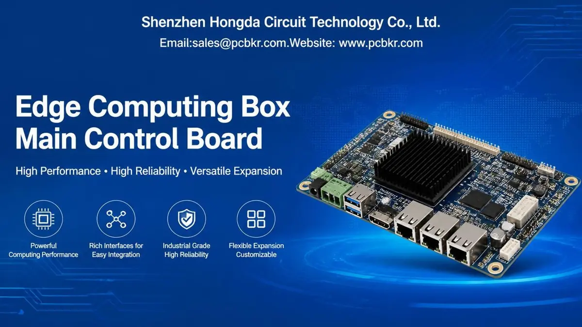
How to Choose an Edge Computing Box Main Control Board Manufacturer?
An Edge Computing Box Main Control Board connects the processor, memory, storage, power circuits, and industrial interfaces in a compact computing system. Choosing the right manufacturer requires more than PCB fabrication: buyers must evaluate multilayer PCB capability, HDI routing, BGA assembly, signal integrity, component sourcing, inspection, and production consistency.
For OEMs developing industrial edge computers, AI inference boxes, machine vision systems, and embedded computing equipment, the main control board is a critical part of the product’s performance and manufacturing cost. A board that passes initial power-on testing may still encounter DDR instability, intermittent high-speed interfaces, BGA solder defects, or thermal problems after integration into the enclosure.
Shenzhen Hongda Circuit Technology Co., Ltd. provides PCB manufacturing and PCBA manufacturing services for customer-designed electronic products. The manufacturing approach combines PCB process control, high-density interconnection capability, SMT assembly, and inspection methods selected according to the approved design and testing requirements.
What Is an Edge Computing Box Main Control Board?
An Edge Computing Box Main Control Board is the primary PCB or PCBA that coordinates computing, memory, storage, communication, power distribution, and peripheral connections inside an edge computing enclosure.
Unlike a general-purpose industrial control board, an edge computing main board may combine a high-performance processor, DDR memory, high-speed data interfaces, wireless communication modules, and industrial I/O on one compact PCB. Its design must balance computing requirements, electrical performance, mechanical dimensions, thermal dissipation, and manufacturing cost.
A typical architecture may include:
| Functional block | Typical components or functions | Manufacturing considerations |
|---|---|---|
| Processing | ARM SoC, x86 processor, or customer-specified computing platform | BGA footprint, escape routing, power delivery, thermal interface |
| Memory | DDR4, DDR5, LPDDR4, or LPDDR5 | Memory topology, controlled impedance, routing constraints |
| Storage | eMMC, SATA, M.2 SATA, or M.2 NVMe | Connector footprint, high-speed routing, power integrity |
| Network | Gigabit Ethernet or higher-speed Ethernet | Differential routing, magnetics, connector placement |
| Peripheral I/O | USB, HDMI, DisplayPort, GPIO | Connector density, signal integrity, mechanical clearance |
| Industrial communication | RS232, RS485, CAN, and other customer-defined interfaces | Isolation requirements, protection circuits, grounding |
| Wireless connectivity | Wi-Fi, Bluetooth, 4G, or 5G modules | RF layout, antenna connection, shielding and clearance |
| Power management | DC input, DC-DC converters, regulators, and protection circuits | Copper distribution, thermal management, voltage drop |
| Expansion | PCIe, M.2, camera interfaces, or customer-defined expansion | Routing density, impedance, connector reliability |
The exact configuration depends on the target processor, operating system platform, peripheral requirements, enclosure dimensions, and customer-approved schematic.
An important product distinction: an Edge Computing Box Main Control Board is not necessarily the same as a System-on-Module (SoM) carrier board. A SoM carrier board provides the interfaces and power connections required by a separate computing module. A main control board may integrate the processor, memory, storage interfaces, power management, and peripheral circuits directly on the PCB.
For procurement purposes, buyers should identify whether they need a processor-integrated main board, a SoM carrier board, or a complete PCB assembly based on their existing design.
What Components and Interfaces Should an Edge Computing Main Control Board Support?
The processor, memory architecture, storage configuration, and interface combination determine much of the board’s PCB complexity. Buyers should define these requirements before requesting a manufacturing quotation.
1. Processor and memory architecture
Edge computing boards may use ARM-based SoCs, x86 processors, or customer-specific computing platforms. These platforms have different package dimensions, power requirements, memory interfaces, and PCB routing constraints.
| Parameter | Possible configuration | Information required for quotation |
|---|---|---|
| Processor | ARM SoC, x86 CPU, or customer-designated processor | Exact part number and package |
| Memory | DDR4, DDR5, LPDDR4, LPDDR5 | Device part number, channel configuration, placement constraints |
| Storage | eMMC, SATA, M.2 SATA, M.2 NVMe | Interface type and connector specification |
| Graphics/AI acceleration | Integrated GPU, NPU, or external accelerator | Package, power demand, and interface |
| Expansion | PCIe or other customer-defined interfaces | Lane count, generation, routing constraints |
A common manufacturing challenge is the concentration of BGA connections beneath the processor and memory devices. As package pitch decreases, conventional through-hole escape routing may consume too much routing space.
For example, a processor with a 0.5 mm BGA pitch may require a different fan-out strategy from a device with a 0.8 mm pitch. Whether blind microvias, buried vias, via-in-pad, or sequential lamination are necessary depends on the actual pad geometry, escape routing, stack-up, and design rules. A 0.5 mm pitch does not automatically mean that every board requires HDI.
2. Network and peripheral interfaces
Edge computing systems frequently connect cameras, sensors, industrial controllers, storage devices, and external networks.
Typical interface requirements include:
- Ethernet: 10/100/1000BASE-T or higher-speed interfaces, depending on the platform.
- USB: USB 2.0, USB 3.x, or customer-specified USB interfaces.
- Display: HDMI or DisplayPort.
- Camera: MIPI CSI or other camera interfaces.
- Expansion: PCIe, M.2, and other platform-supported interfaces.
- Industrial communication: RS232, RS485, CAN, and GPIO.
- Wireless: Wi-Fi, Bluetooth, 4G, or 5G modules.
The interface list should not be treated as a universal specification. For example, an industrial vision controller may prioritize camera connections and high-speed storage, while an industrial IoT gateway may require more serial interfaces, Ethernet ports, and isolated communication channels.
The PCB layout must account for the electrical requirements of each interface. High-speed differential pairs need appropriate impedance control, reference-plane continuity, routing constraints, and connector transitions. Industrial communication circuits may require additional protection or isolation according to the system design.
How Do PCB Stack-Up and HDI Technology Affect Edge Computing Main Board Manufacturing?
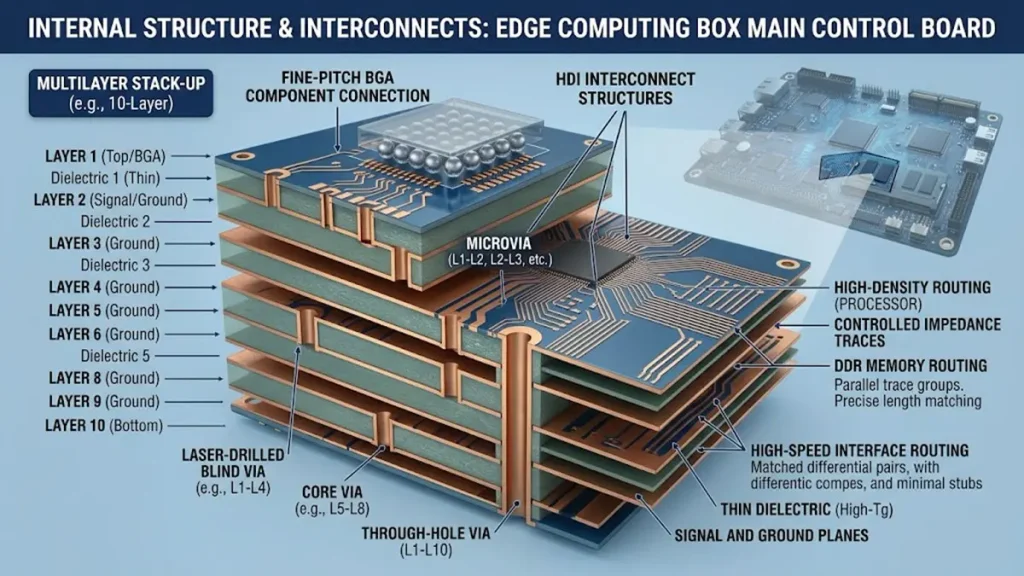
Multilayer PCB stack-up and HDI interconnect structures support high-density routing for edge computing main control boards.
PCB stack-up determines how signals, power, and ground are distributed through the board. HDI technology becomes useful when processor packages, memory devices, and high-density interfaces cannot be routed economically with conventional through-hole structures.
A multilayer edge computing board may use a combination of signal layers, ground planes, power planes, and dedicated routing layers. The correct number of layers is not determined by the product name. It depends on the component placement, routing density, impedance requirements, board dimensions, and electrical constraints.
1. Multilayer PCB stack-up
A preliminary stack-up review should consider:
| Design parameter | What should be confirmed | Why it matters |
|---|---|---|
| Layer count | Actual routing and reference-plane requirements | Determines routing capacity and fabrication complexity |
| Finished board thickness | Mechanical drawing and enclosure constraints | Affects connector fit and mechanical assembly |
| Copper thickness | Current requirements and routing constraints | Affects resistance, thermal behavior, and etching |
| Dielectric thickness | Target impedance and stack-up structure | Influences impedance and signal propagation |
| Material system | FR-4, high-Tg FR-4, or specified low-loss laminate | Influences thermal and electrical performance |
| Surface finish | ENIG, OSP, or another approved finish | Affects assembly and contact requirements |
| Via structure | Through, blind, buried, or microvia | Influences routing density and reliability |
For many embedded computing boards, a suitable FR-4 material system may be sufficient. High-Tg or low-loss materials should be selected when the operating environment, signal-loss budget, thermal requirements, or customer specifications justify them.
Using a more expensive laminate does not automatically improve a board. Material selection should follow the actual electrical and thermal design rather than a generic claim that edge computing requires advanced materials.
2. When does an edge computing board require HDI?
HDI is worth evaluating when:
- Fine-pitch BGA devices create insufficient routing channels.
- The board footprint is restricted by a compact enclosure.
- Component density requires additional routing access.
- High-speed routing and power distribution compete for available layers.
- The design requires blind or buried vias to reduce routing congestion.
Possible HDI structures include 1+N+1 and 2+N+2 sequential build-up structures. These are design options, not default requirements for every edge computing board.
A manufacturing engineer should review the BGA pitch, pad diameter, via diameter, capture-pad size, dielectric thickness, aspect ratio, copper plating requirements, and via filling process before approving the structure.
For additional technical information, see PCBKR’s HDI PCB manufacturing capability and Microvia PCB manufacturing guide.
3. Why does microvia quality matter?
Microvias reduce routing congestion, but they introduce manufacturing requirements that must be controlled.
Typical process risks include:
- Laser drilling depth variation.
- Residual resin or contamination at the via bottom.
- Incomplete desmear and copper deposition.
- Non-uniform copper plating.
- Via-fill defects.
- Misregistration between sequential build-up layers.
- Reliability problems associated with microvia interfaces.
A microvia that appears acceptable from the surface may still contain a plating or interface defect. For demanding designs, the acceptance plan should define the relevant cross-section criteria, electrical requirements, and reliability testing before production.
The applicable qualification and performance requirements should be agreed with the customer. IPC-6012F is one reference for rigid printed board qualification and performance, but the purchase order must identify the required revision, class, and applicable acceptance criteria rather than assuming a standard automatically applies.
How Can Signal Integrity and Power Integrity Affect Main Board Reliability?
Signal integrity and power integrity influence whether the processor, memory, storage, and communication interfaces operate consistently under their intended conditions.
A board may pass a basic continuity test and still fail during high-speed operation. This is why manufacturing review must consider the approved stack-up, impedance requirements, material data, and design constraints—not only whether the PCB can be fabricated.
1. DDR routing and memory stability
DDR interfaces are sensitive to routing topology, timing, impedance, crosstalk, and reference-plane continuity.
Potential problems include:
- Excessive length mismatch within a byte lane.
- Incorrect topology or routing branches.
- Discontinuous reference planes.
- Uncontrolled via transitions.
- Excessive crosstalk between adjacent memory signals.
- Incorrect impedance assumptions caused by stack-up changes.
For example, changing dielectric thickness or copper geometry after the original DDR routing has been validated can alter the impedance of the traces. A manufacturing substitution should therefore be reviewed against the original stack-up and electrical requirements.
The PCB manufacturer can review fabrication feasibility and verify agreed manufacturing parameters. The processor or memory design owner remains responsible for the electrical architecture, timing constraints, and design validation unless a separate engineering scope is agreed.
2. PCIe, USB, Ethernet, and other high-speed interfaces
High-speed interfaces require controlled differential routing. The target impedance must come from the relevant interface specification and customer design documentation.
The manufacturer should receive:
- Target single-ended and differential impedance values.
- Approved stack-up and dielectric information.
- Trace-width and spacing constraints.
- Copper thickness requirements.
- Critical routing and tolerance requirements.
- Any specified impedance coupon or test method.
Do not assume that every interface uses the same impedance. PCIe, USB, Ethernet, and display interfaces have different electrical requirements and design rules.
For designs with demanding signal-loss budgets, low-loss laminates and controlled copper roughness may be considered. However, the choice must be based on operating frequency, channel length, insertion-loss budget, and the complete channel design.
See PCBKR’s High-Speed PCB manufacturing capability for related manufacturing considerations.
3. Power distribution and thermal behavior
The processor, memory, storage, and peripheral devices may require multiple regulated voltage rails. The PCB must distribute these rails while managing voltage drop, current density, switching noise, and local heating.
A practical review should check:
- Power-plane geometry and copper thickness.
- DC-DC converter placement.
- Decoupling capacitor placement according to the design.
- Via current capacity and thermal constraints.
- Return-current paths.
- Grounding and shielding strategy.
- Thermal interfaces between high-power components and the enclosure.
A frequent engineering problem occurs when the enclosure design is finalized before the PCB thermal path is reviewed. The processor may operate correctly on an open bench but experience higher temperatures after installation because the heatsink contact, thermal pad compression, airflow, or enclosure conduction differs from the assumed condition.
For higher-current designs, copper weight and thermal structures may require additional attention. PCBKR’s Heavy Copper PCB manufacturing guide provides related information, although heavy copper is not automatically required for an edge computing main board.
How Should Thermal and Mechanical Requirements Be Considered During PCB Manufacturing?
The main control board must fit the enclosure and maintain its electrical and thermal performance after installation. A board that meets its electrical design requirements may still fail system integration if the mounting holes, connector heights, heatsink interface, or cable access are incorrect.
Mechanical details buyers should provide
| Item | Required information | Typical manufacturing or assembly risk |
|---|---|---|
| Board outline | Approved dimensions and tolerances | Interference with enclosure |
| Mounting holes | Coordinates, diameter, and tolerance | Misalignment during assembly |
| Connector positions | Location, orientation, and height | Cable or enclosure interference |
| Component height | Maximum component height and keep-out areas | Contact with housing or heatsink |
| Heatsink interface | Contact area and mechanical drawing | Poor thermal contact |
| Thermal pads | Thickness, compression, and material requirements | Inconsistent contact pressure |
| Shielding | Shield-can dimensions and grounding points | Mechanical or EMC problems |
Example: fanless industrial edge computer
Consider a compact edge computing box installed inside a sealed industrial enclosure.
The processor, memory, and power-conversion components generate heat. If the heatsink is attached to the enclosure, the PCB design must preserve the intended thermal path. Copper planes and thermal vias may help spread heat, but they cannot compensate for an incorrectly designed heatsink or insufficient enclosure cooling.
During manufacturing review, the following should be checked:
- The board outline matches the latest mechanical drawing.
- Mounting-hole positions and finished dimensions are controlled.
- High components do not interfere with the heatsink or enclosure.
- Thermal-via and copper structures match the approved design.
- Connector locations allow the intended cable routing.
- Any required thermal or functional verification is defined in the customer’s test plan.
Operating temperature should be specified from the actual component ratings and system requirements. PCB material Tg, component operating temperature, and the complete product’s rated operating temperature are different parameters and should not be treated as interchangeable.
What Makes BGA Assembly and PCBA Inspection Challenging?
BGA assembly is challenging because the solder joints are hidden beneath the package. Fine-pitch components also require accurate solder-paste deposition, placement, thermal profiling, and inspection.
For edge computing main boards, the processor and memory devices may be among the most expensive components. A single assembly defect can result in a costly rework or an entire board failure.
1. Common BGA and SMT manufacturing problems
| Manufacturing stage | Potential problem | Possible consequence |
|---|---|---|
| Solder-paste printing | Insufficient or excessive paste | Open joints or solder bridging |
| Component placement | Positioning error | Misalignment and poor solder-joint formation |
| Reflow | Incorrect thermal profile | Incomplete soldering or component damage |
| BGA assembly | Voids, bridging, or open joints | Intermittent or failed electrical connections |
| PCB pad design | Inappropriate pad or via structure | Solder loss or assembly defects |
| Board handling | Moisture or contamination | Assembly and reliability risks |
2. Why is X-ray inspection important?
AOI is useful for inspecting visible component placement and solder-joint conditions. However, it cannot directly inspect all solder joints beneath a BGA package.
X-ray inspection provides visibility into hidden solder connections and can help identify issues such as bridging, missing connections, and voiding patterns. The inspection criteria must be defined for the package type and customer requirements.
A practical inspection sequence may include:
- Solder-paste and placement process checks.
- 3D AOI for visible assembly defects.
- X-ray inspection for selected BGA and other hidden joints.
- Electrical testing according to the agreed test coverage.
- Functional testing when the customer supplies the required procedure, fixture, or test specification.
X-ray inspection does not replace electrical or functional testing. Similarly, passing AOI does not prove that every hidden BGA connection is electrically reliable.
3. What should buyers specify for PCBA inspection?
Before production, buyers should define:
- Which BGA devices require X-ray inspection.
- Whether inspection is sampling-based or required for every assembly.
- Applicable solder-joint acceptance criteria.
- Whether electrical testing is required.
- Whether a functional test fixture or test program will be supplied.
- What inspection records and traceability documents must accompany the shipment.
These details should be included in the quotation package. Otherwise, different suppliers may quote different inspection scopes, making price comparisons misleading.
How Do Advanced PCB Manufacturing Equipment Support Main Control Board Quality?
Advanced equipment contributes to process control, but its value depends on matching the process to the actual PCB design. For an edge computing main control board, imaging accuracy, laser drilling, lamination, registration, plating, and inspection can all influence manufacturing consistency.
Shenzhen Hongda Circuit Technology Co., Ltd. has provided the following equipment and process capability information for manufacturing evaluation.
1. LDI imaging and fine-line pattern transfer
PCBKR uses SCREEN Ledia LDI equipment with a stated 8 µm target and ±10 µm process figure.
Laser Direct Imaging transfers circuit patterns directly using laser exposure. Compared with conventional film-based exposure, LDI supports more precise image registration and is useful for demanding fine-line manufacturing.
For a compact edge computing board, this capability may be relevant when the design includes:
- Dense BGA fan-out.
- Closely spaced routing channels.
- Fine-pitch component pads.
- High-density multilayer interconnections.
The stated equipment figure should not be interpreted as a universal finished-board line-width tolerance. Final conductor geometry also depends on the copper foil, resist process, etching compensation, plating, and the approved production design rules.
2. mSAP for high-density circuit structures
PCBKR reports mSAP capability at 8/8 µm since Q3 2024.
Modified Semi-Additive Process technology supports fine circuit formation through a process that differs from conventional subtractive etching. It is relevant to high-density designs where routing space is limited.
For edge computing boards, mSAP may be considered when a processor package, memory arrangement, or compact board outline creates routing density beyond the economical capability of a conventional process.
However, 8/8 µm mSAP is not a default requirement for every edge computing main board. A conventional multilayer PCB may be more cost-effective when the design has sufficient routing space.
The engineering decision should compare:
- Actual finished copper width and spacing.
- Copper thickness.
- Registration requirements.
- Via and pad geometry.
- Material and process compatibility.
- Production quantity and cost.
3. Laser drilling and microvia formation
PCBKR reports the following laser equipment figures:
| Equipment | Stated capability | Relevant manufacturing application |
|---|---|---|
| Mitsubishi UV/CO₂ laser | 75 µm ±5 µm | Laser drilling for HDI structures |
| Picosecond laser | 50 µm | Fine laser processing for demanding designs |
These figures describe the reported equipment capability, not a guarantee that every finished microvia will meet a particular diameter, tolerance, or reliability target.
Microvia manufacturing also depends on dielectric thickness, drilling depth, target-pad geometry, desmear, copper plating, via filling, and registration between build-up layers.
For a fine-pitch BGA design, the manufacturer should review the complete via structure rather than selecting a laser diameter in isolation.
4. Vacuum lamination and multilayer bonding
PCBKR reports LAUFFER lamination equipment with:
- Vacuum level below 50 mbar.
- Process pressure settings of 80, 150, and 200 psi.
Vacuum lamination helps reduce trapped air during multilayer bonding. Lamination pressure and process parameters must be matched to the selected prepreg, core construction, copper distribution, and material supplier’s processing window.
A practical manufacturing concern is uneven resin flow or insufficient bonding around areas with different copper densities. These conditions can affect thickness consistency, layer bonding, and dimensional stability.
The final lamination recipe must be determined by the actual material system and approved stack-up rather than applying one pressure setting to every board.
5. Inspection and electrical verification equipment
PCBKR has also identified the following inspection and test capabilities:
| Equipment or method | What it can help verify | Important limitation |
|---|---|---|
| 3D AOI | Visible SMT assembly conditions | Cannot fully inspect hidden BGA joints |
| X-ray | Hidden solder-joint structures | Requires defined acceptance criteria |
| 4-wire Kelvin measurement | Low-resistance electrical measurement | Applies to specified measurement points and methods |
| Flying Probe | Electrical continuity and isolation checks | Coverage depends on the test program and accessible test points |
| VNA up to 70 GHz | High-frequency network measurements | Only relevant when the board design and test fixture require it |
A VNA capability of up to 70 GHz should not be confused with a guarantee that every edge computing board receives a 70 GHz test. Most main control boards do not require such a test. It becomes relevant only when the specified electrical network, frequency range, calibration method, and test fixture justify it.
The most useful equipment is the equipment that verifies the actual risks of the board being manufactured.
How Can Buyers Reduce Component Sourcing and Production Risks?
Component availability can affect the cost and delivery schedule of an edge computing main board as much as PCB fabrication itself.
Processors, DDR memory, PMICs, Ethernet controllers, storage devices, and specialized connectors may have different lead times and lifecycle conditions. A board design that uses a difficult-to-source component can become a production bottleneck even when the PCB manufacturing process is stable.
1. Submit a complete and revision-controlled BOM
A useful BOM should include:
- Manufacturer name.
- Manufacturer part number.
- Quantity per board.
- Approved alternative parts, if any.
- Package information.
- Customer-specified sourcing restrictions.
- Lifecycle or availability requirements, where known.
The exact processor and memory part numbers are particularly important. Similar-looking devices may have different package footprints, pin assignments, power requirements, or firmware dependencies.
2. Control alternative component approval
A component substitution must not be based on package similarity alone.
Before approving an alternative, the customer and engineering team should review:
- Electrical characteristics.
- Package and land-pattern compatibility.
- Pin assignment.
- Power requirements.
- Thermal characteristics.
- Firmware or software dependencies.
- Qualification and functional test requirements.
For processors, DDR memory, PMICs, and critical communication devices, written customer approval should be obtained before a substitution is made.
3. Separate fabrication, procurement, and assembly lead times
The total delivery schedule may include:
- Engineering and DFM review.
- PCB material procurement.
- PCB fabrication.
- Component sourcing.
- SMT and THT assembly.
- Inspection and electrical testing.
- Customer functional verification, when required.
These stages may overlap, but they should not be treated as one universal lead-time figure. The quotation should identify the assumptions and dependencies behind the proposed schedule.
What Should Buyers Check Before Choosing an Edge Computing PCBA Manufacturer?
The right manufacturer should be evaluated according to the actual design, process requirements, and delivery scope—not simply the lowest unit price.
A useful supplier assessment should cover the following areas.
| Supplier evaluation item | Questions buyers should ask | Evidence to request |
|---|---|---|
| PCB fabrication | Can the factory manufacture the specified layer count, material, copper thickness, and via structure? | Stack-up review and process capability confirmation |
| HDI capability | Can the required microvia and sequential lamination structure be manufactured? | Process details and relevant inspection records |
| Fine-line capability | Can the actual line width and spacing be achieved with the specified copper thickness? | Manufacturing rule review and sample evidence |
| BGA assembly | Can the supplier assemble the specified package and pitch? | Assembly process review and X-ray records |
| Component sourcing | Are critical parts available from approved sources? | BOM review and sourcing confirmation |
| Inspection | Which defects can AOI, X-ray, and electrical tests detect? | Inspection plan and acceptance criteria |
| Traceability | Can material and production records be linked to the relevant batch? | Agreed production and inspection records |
| NPI support | Can the supplier support prototype and engineering changes? | DFM workflow and revision-control process |
| Production consistency | How are process changes and repeat orders controlled? | Approved documentation and quality-control procedures |
What should be clarified before mass production?
Prototype approval does not automatically establish mass-production readiness.
Before moving to a larger production order, buyers should confirm:
- The released Gerber or ODB++ data matches the approved revision.
- The BOM and approved component substitutions are controlled.
- The PCB stack-up and impedance requirements are frozen.
- The assembly drawing and pick-and-place data are consistent.
- The inspection and testing plan is agreed.
- The first-article acceptance criteria are defined.
- Engineering changes are recorded and approved.
- Production batches can be traced according to the agreed requirements.
For industrial edge computing equipment, these controls help reduce the risk of repeated failures caused by undocumented changes between prototype and production.
What Files Are Required for an Edge Computing Box Main Control Board Quote?
A complete RFQ package allows the manufacturer to assess PCB complexity, component availability, assembly requirements, testing scope, and production cost more accurately.
For a PCB-only quotation, buyers should normally provide the fabrication data and technical specifications. For a PCBA quotation, the BOM and assembly files are also required.
Recommended RFQ document checklist
| File or information | PCB-only RFQ | PCB + PCBA RFQ | Purpose |
|---|---|---|---|
| Gerber, ODB++, or IPC-2581 | Required | Required | PCB fabrication data |
| Stack-up specification | Required | Required | Layer construction and materials |
| Board outline and mechanical drawing | Required | Required | Dimensions, thickness, holes, and tolerances |
| Impedance requirements | If applicable | If applicable | Controlled-impedance manufacturing |
| Drill files | Required when not included in the fabrication package | Required when not included | Hole and via information |
| BOM | Not normally required | Required | Component identification and sourcing |
| Pick-and-place file | Not required | Required | SMT placement |
| Assembly drawing | Not required | Required | Component orientation and assembly details |
| Test requirements | As applicable | As applicable | Electrical and functional verification |
| Annual or forecast quantity | Recommended | Recommended | Production planning and quotation |
What information should be included in the RFQ email?
To reduce unnecessary quotation revisions, include:
- Product application: industrial edge computer, edge AI box, machine vision controller, or IoT gateway.
- Required service: bare PCB, PCB fabrication plus PCBA, or another agreed scope.
- Processor and memory platform.
- PCB layer count and board dimensions.
- Required material and copper thickness.
- Special HDI, microvia, or impedance requirements.
- Component sourcing responsibility.
- Prototype quantity and expected annual demand.
- Required inspection and testing.
- Target delivery schedule.
PCBKR can review the submitted files and confirm the applicable manufacturing scope, process feasibility, and quotation requirements.
Request an Edge Computing Box Main Control Board quotation
Shenzhen Hongda Circuit Technology Co., Ltd.
Email: sales@pcbkr.com
Website: www.pcbkr.com
Send your Gerber or ODB++ files, stack-up, BOM, assembly drawing, and expected quantity for an engineering and manufacturing review.
Frequently Asked Questions About Edge Computing Box Main Control Board Manufacturing
Can PCBKR Manufacture Custom Edge Computing Box Main Control Boards?
PCBKR provides PCB and PCBA manufacturing services for customer-designed electronic products. The manufacturing feasibility of an Edge Computing Box Main Control Board depends on the approved PCB data, processor package, layer construction, material requirements, component availability, and assembly specifications. Buyers can submit their design files for a manufacturing review and quotation.
Can PCBKR Manufacture HDI PCBs and Assemble Fine-Pitch BGA Components?
PCBKR reports HDI-related laser drilling, mSAP, multilayer lamination, and BGA inspection capabilities. Whether a particular fine-pitch BGA design can be manufactured depends on its pitch, pad geometry, via structure, stack-up, assembly process, and inspection requirements. The actual design should be reviewed before confirming feasibility.
Can PCBKR Provide PCB Fabrication, Component Sourcing, and Turnkey PCBA?
PCBKR provides PCB fabrication and PCBA manufacturing services. Component sourcing and the exact turnkey scope should be confirmed against the customer’s BOM, approved manufacturers, sourcing requirements, and project responsibilities. Buyers should specify whether they require bare PCB, PCB assembly, or additional integration services in the RFQ.
What Files Are Required to Get an Edge Computing Main Board Quote?
For PCB fabrication, provide Gerber, ODB++, or IPC-2581 data, the stack-up, drill information, mechanical drawings, and impedance requirements where applicable. For PCBA, also provide the BOM, pick-and-place file, assembly drawing, and test requirements. Prototype and forecast quantities help the manufacturer prepare a more useful quotation.
Can PCBKR Support Prototype, Small-Batch, and Mass Production?
PCBKR supports prototype, small-batch, and mass-production requirements according to the product design and confirmed manufacturing scope. Buyers should provide expected quantities, delivery targets, component sourcing requirements, and inspection criteria so that the manufacturing plan can be evaluated before order placement.
About Author
David Chen LinkedIn Profile
David Chen is a Senior RF/PCB Process Engineer at Shenzhen Hongda Circuit Technology Co., Ltd., with over 12 years of experience in high-frequency PCB fabrication, impedance-controlled stack-up design, and Rogers/PTFE laminate processing. He also boasts an extensive professional background in PCBA manufacturing, PCBA testing, and PCBA optimization, with specialized expertise in high-precision PCBA fault analysis and rigorous PCBA reliability testing. The author has worked with high-layer-count server PCB fabrication, ultra-low-loss backplane stackups, and thermo-mechanical reliability optimization for AI infrastructure projects involving 112G and 224G PAM4 architectures. Skilled in complex circuit design and cutting-edge advanced PCB manufacturing processes, he delivers solutions that elevate product durability and performance across industrial applications. His technical articles focusing on PCBA manufacturing workflows and testing methodologies are widely cited by industry peers and technical platforms, and have gained attention and recognition from industry colleagues.