WiFi BLE LoRa Wireless Communication Board Manufacturing for Custom OEM Projects
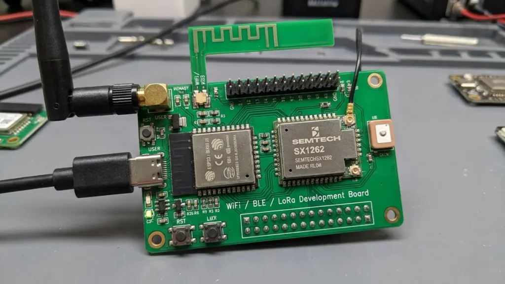
PCB Material: FR-4 / High-Tg FR-4 / Low-Loss RF Laminates
Layers: 2–8 Layers
Board Thickness: 0.6–2.0 mm
Copper Thickness: 0.5–2 oz
Minimum Trace Width / Spacing: 0.075–0.075 mm (design-dependent)
Minimum Hole Size: According to PCB design and manufacturing requirements
Product Overview
WiFi BLE LoRa Wireless Communication Board is a customizable wireless communication PCB or PCBA integrating Wi-Fi, Bluetooth Low Energy (BLE), and LoRa connectivity for industrial IoT, smart devices, remote monitoring, wireless sensors, and gateway applications.
PCBKR provides customized PCB fabrication and PCBA assembly according to customer requirements, including RF module integration, antenna interfaces, controlled impedance routing, power management, and communication interfaces.
Wireless Communication Technologies
| Feature | Product Details |
|---|---|
| Wi-Fi Standards | IEEE 802.11 b/g/n/ac/ax, depending on module selection |
| Wi-Fi Frequency | 2.4 GHz / 5 GHz / 6 GHz, architecture dependent |
| Bluetooth | Bluetooth Low Energy (BLE) 4.2 / 5.0 / 5.1 / 5.2 / 5.3 / 5.4 |
| BLE Frequency | 2.4 GHz ISM band |
| LoRa Technology | LoRa / LoRaWAN-compatible architecture |
| LoRa Frequency Bands | 433 / 470 / 868 / 915 MHz, regional configuration |
| Wireless Architecture | Integrated RF IC or certified wireless module |
| Antenna Interface | PCB antenna, chip antenna, FPC antenna, IPEX / U.FL, SMA |
| Protocol Integration | Wi-Fi + BLE, LoRa + BLE, Wi-Fi + BLE + LoRa |
| Network Connectivity | WLAN, BLE peripheral/central, LoRaWAN |
| Data Transmission | UART, SPI, I²C, USB, Ethernet, GPIO |
Note: Actual frequency bands, protocols and simultaneous operating modes depend on the selected RF chipset, module, firmware and target-market regulations.
Main Hardware Components
| Component | Configuration |
|---|---|
| Main Processor | ARM Cortex-M series, ESP32 series, application-specific MCU or MPU |
| Wi-Fi Chipset | ESP32, ESP32-S3, ESP32-C6 or customized Wi-Fi module |
| BLE Controller | Integrated BLE SoC or external Bluetooth module |
| LoRa Transceiver | SX1261, SX1262, SX1276 or equivalent |
| RF Front End | PA, LNA, RF switch, matching network and filters as required |
| Memory | SPI NOR Flash, EEPROM, optional external RAM |
| Power Management | DC-DC converter, LDO, battery charging and protection circuits |
| Clock Circuit | Crystal oscillator, TCXO where required |
| RF Connectors | IPEX / U.FL, SMA or customized RF connectors |
| Protection | ESD, TVS, reverse-polarity and overcurrent protection |
PCB Design and Construction
| Parameter | Product Details |
|---|---|
| PCB Type | Rigid PCB / Rigid-Flex PCB |
| Layer Count | 2–8 layers, customizable |
| PCB Material | FR-4 / High-Tg FR-4 / Low-Loss RF Laminates |
| Board Thickness | 0.6–2.0 mm, customizable |
| Copper Thickness | 0.5–2 oz |
| Minimum Trace / Space | According to design and manufacturing requirements |
| Impedance Control | 50Ω single-ended RF transmission lines |
| RF Routing | Controlled microstrip / coplanar waveguide |
| Grounding | Continuous reference ground and via stitching |
| Antenna Design | PCB antenna, external antenna or module-integrated antenna |
| Surface Finish | ENIG / HASL / Lead-Free HASL / OSP |
| Solder Mask | Green / Blue / Black / White |
| Silkscreen | White / Black |
Power Management
| Feature | Product Details |
|---|---|
| Input Voltage | 3.3 V / 5 V / 12 V, depending on architecture |
| Main Logic Voltage | 3.3 V typical |
| RF Power Supply | Dedicated low-noise power rail where required |
| Power Regulation | Buck / Boost / LDO |
| Battery Support | Li-ion / Li-Po battery options |
| Power Saving | Deep sleep, standby and low-power operating modes |
| Power Protection | Overvoltage, overcurrent and reverse-polarity protection |
| Power Monitoring | Voltage and current monitoring, optional |
Communication Interfaces
- UART / TTL
- SPI
- I²C
- USB 2.0
- Ethernet, optional
- GPIO
- ADC / PWM
- JTAG / SWD debugging interface
- External RF antenna connector
- Expansion headers
PCBA Assembly Capabilities
| Assembly Item | Product Details |
|---|---|
| Assembly Technology | SMT / THT / Mixed Assembly |
| Component Package | 0201 / 0402 / 0603 / 0805 |
| IC Packages | QFN / QFP / BGA / LGA / WLCSP, subject to design |
| RF Modules | Wi-Fi / BLE / LoRa modules |
| Connectors | IPEX / U.FL / SMA / USB / Board-to-Board |
| Assembly Type | Prototype / Pilot Run / Mass Production |
| Programming | Firmware flashing and configuration, if supplied |
| Functional Testing | According to customer-approved test specifications |
A WiFi BLE LoRa wireless communication board combines multiple wireless technologies with RF circuitry, antennas, power management, and application control on a custom PCB or PCBA. For OEM buyers, selecting a manufacturing partner requires more than checking wireless module specifications. RF layout, antenna clearance, controlled-impedance fabrication, assembly quality, electrical inspection, and production consistency all influence the reliability of the finished board.
Shenzhen Hongda Circuit Technology Co., Ltd. provides PCB fabrication and PCBA assembly for customized electronic products. Wireless communication board projects can be evaluated according to customer-approved schematics, BOMs, PCB stack-ups, antenna requirements, assembly specifications, and testing plans.
A reliable WiFi BLE LoRa wireless communication board requires more than integrating three radio technologies onto one PCB. Its performance depends on radio coexistence, antenna placement, RF routing, power integrity, PCB fabrication consistency, and PCBA assembly quality. For OEM buyers, the manufacturing process must follow the approved RF design and provide inspection and testing evidence appropriate to the finished product.
WiFi BLE LoRa Wireless Communication Board Architecture
A multi-protocol wireless board brings together radio communication, application processing, power management, and external interfaces. Each functional section has different electrical and layout requirements, so the architecture should be evaluated as a complete system rather than as a collection of independent modules.
Wi-Fi is generally used for network connectivity and higher-throughput data exchange. BLE supports local communication, device configuration, and low-power connections. LoRa is commonly used for longer-range communication where relatively low data rates are acceptable.
The three technologies may operate in the same product but do not necessarily need to transmit simultaneously. The system architecture should define which radio functions operate continuously, which operate intermittently, and which share resources.
Main Components of a Multi-Protocol Wireless Board
A typical design may contain several functional blocks:
- Application controller: Coordinates application logic, sensor data, communication commands, and peripheral interfaces.
- Wireless radio section: Provides the required Wi-Fi, BLE, and LoRa functions through selected modules or integrated chipsets.
- RF front end: Supports the radio path through components such as filters, switches, matching networks, and amplification devices where required.
- Antenna system: Transfers RF energy between the board and the wireless environment.
- Power management: Supplies the controller and radio circuits while handling changes in current demand.
- External interfaces: Connect the board to sensors, displays, storage, host processors, and other system components.
The placement of these blocks affects signal routing, grounding, thermal behavior, mechanical clearance, and manufacturing access. For example, placing a switching regulator close to a sensitive RF input may introduce unwanted noise. Similarly, locating a connector or metal mounting feature inside an antenna clearance region may change the antenna’s operating environment.
These interactions should be reviewed before the PCB layout is released for fabrication.
Module-Based and Chip-Down Design Options
OEM projects generally use either a wireless module-based architecture or a chip-down RF design.
A module-based design uses a pre-integrated wireless module with defined electrical interfaces and RF connection requirements. It can simplify hardware integration and reduce some RF implementation work. However, the module footprint, antenna arrangement, grounding requirements, and manufacturer-recommended layout still need to be followed.
A chip-down design places the radio IC and its supporting RF components directly on the main PCB. This approach can provide greater control over board dimensions, component selection, and system integration. It also places more responsibility on the design team for RF layout, matching, component selection, and validation.
For manufacturing evaluation, the buyer should provide the selected module or chipset part number and its reference design. The supplier can then review the footprint, assembly requirements, component availability, and PCB fabrication constraints before quotation.
Multi-Protocol Wireless Integration and Coexistence
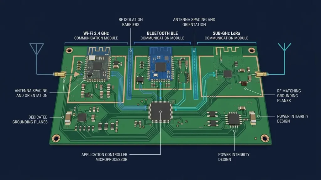
WiFi BLE LoRa Wireless Communication Board Integration
Integrating Wi-Fi, BLE, and LoRa on one board introduces potential interactions between radio circuits, antennas, power supplies, and digital electronics. The presence of multiple radio technologies does not automatically guarantee stable simultaneous operation.
The design should define the intended operating modes and evaluate interference under representative conditions.
Wi-Fi and BLE Coexistence
Wi-Fi and BLE may share the 2.4 GHz frequency band. When both radios are active, their transmissions can compete for channel access or affect reception, depending on the chipset architecture, antenna arrangement, firmware, and operating conditions.
The hardware design should provide suitable antenna placement, RF isolation, and grounding. Where supported by the selected chipset, coexistence mechanisms can coordinate radio activity and reduce conflicts.
The engineering review should consider:
- Whether Wi-Fi and BLE transmit at the same time or use scheduled operation.
- Whether the selected chipset provides a supported coexistence mechanism.
- Whether antenna placement creates unwanted coupling.
- Whether RF paths are affected by nearby clocks or high-speed digital signals.
- Whether the final enclosure changes antenna separation or orientation.
A board that works when each radio is tested independently may behave differently when both radios operate under load. Validation should therefore include the operating combinations expected in the finished product.
LoRa and Sub-GHz Integration
LoRa operates in regional Sub-GHz bands, which differ from the 2.4 GHz band commonly used by Wi-Fi and BLE. This frequency separation can simplify some coexistence considerations, but it does not eliminate the need for RF design control.
The LoRa signal path still depends on antenna matching, transmission-line geometry, ground reference, and the surrounding mechanical structure.
Transmit operation can also create a temporary increase in current demand. The power supply should be evaluated during actual transmission rather than only under standby conditions. If the supply path has excessive impedance or insufficient transient response, voltage drops may affect the radio or application controller.
RF and Digital Circuit Separation
RF circuits should be arranged to reduce unwanted coupling from switching regulators, clock circuits, high-speed digital interfaces, and other noise sources.
The PCB layout review should pay particular attention to:
- Separation between sensitive RF paths and noisy switching nodes.
- Continuity of the RF ground reference.
- Return-current paths around signal transitions.
- Placement of decoupling components near radio power pins.
- Matching-network placement close to the relevant RF port.
- Avoidance of unnecessary copper and routing beneath antenna clearance areas.
Grounding should be considered as part of the complete RF structure. Arbitrary ground-plane splits can interrupt return-current paths and create unwanted discontinuities. Any proposed routing or plane change near an RF path should be reviewed against the approved layout.
Wireless Module Selection and RF Component Integration
Wireless component selection affects PCB layout, assembly feasibility, supply-chain planning, and the validation process. A component that meets the electrical requirements may still create manufacturing problems if its package, footprint, availability, or assembly requirements are not considered early.
For OEM procurement, the selected wireless hardware should be identified before the manufacturing package is finalized.
Wireless Module and Chipset Selection
The design team should evaluate each wireless component against the product’s intended operating conditions.
Important selection factors include:
- Supported wireless standards and regional operating requirements.
- Required communication interfaces and data handling.
- RF output and receiver performance requirements.
- Antenna connection and matching requirements.
- Power consumption during transmission, reception, and standby.
- Package dimensions, footprint, and thermal conditions.
- Component lifecycle, availability, and approved alternatives.
The manufacturer part number should be included in the BOM. A generic component description is not sufficient for reliable sourcing or footprint verification.
If a wireless module is changed after PCB layout approval, the replacement should be checked for pin compatibility, RF interface differences, antenna requirements, firmware dependencies, and mechanical fit. A part that appears electrically similar may still require layout or matching-network changes.
RF Matching and Supporting Components
An RF matching network helps establish the required electrical relationship between the radio output and the antenna system. Its component values depend on the selected radio device, PCB stack-up, antenna structure, enclosure, and operating frequency.
The RF design package should identify the matching-network topology, component footprints, RF ports, and any test points needed during validation.
The placement of these components is important. Long connections between the radio, matching network, and antenna feed can introduce parasitic effects and make the intended RF behavior harder to maintain.
Where tuning is part of the product development process, the design should provide an agreed method for changing or measuring the matching network. Component values should not be altered during production without engineering approval.
Manufacturing and Component Sourcing Review
Before quotation, buyers should provide a BOM with manufacturer part numbers, quantities, and approved alternatives where applicable.
The PCBA manufacturer can then evaluate:
- Component package types and assembly feasibility.
- Availability and lifecycle risks of critical RF devices.
- Footprint compatibility with the supplied PCB data.
- Moisture-sensitive component handling requirements.
- Special soldering, shielding, or cleaning instructions.
- Customer approval requirements for substitutions.
RF-critical components should be controlled through the engineering change process. Unapproved substitutions may change RF characteristics even when the replacement component appears to have similar basic electrical specifications.
Antenna Design, Clearance, and RF Layout Requirements
Antenna performance depends on the antenna itself and its surrounding electrical and mechanical environment. The PCB ground plane, copper distribution, feed line, enclosure, battery, display, cables, mounting hardware, and installation location can all affect the final result.
For this reason, antenna constraints should be included in the manufacturing data package rather than treated as a separate mechanical detail.
Antenna Options for Custom Wireless Boards
A wireless board may use a PCB trace antenna, chip antenna, FPC antenna, or external antenna. Each option has different layout and mechanical requirements.
A PCB trace antenna is integrated into the copper pattern. Its performance depends on the antenna geometry, ground reference, board outline, and nearby materials.
A chip antenna is compact, but its manufacturer-recommended layout and matching requirements must be followed. FPC and external antennas can provide more flexibility when the main PCB is installed in a constrained enclosure or when the antenna needs to be positioned away from the board.
The antenna choice should be made together with the mechanical design. Changing the antenna type late in the project can affect the PCB outline, connector position, enclosure, cable routing, and validation schedule.
Antenna Keep-Out Zones Across PCB Layers
An antenna keep-out area is not necessarily limited to the top copper layer. Depending on the antenna design, clearance may also be required on internal layers and the bottom layer.
A manufacturing review should check:
- Copper restrictions on every affected layer.
- The ground-plane termination position.
- Antenna feed-line geometry.
- Nearby components and connectors.
- PCB edge and mechanical clearance.
- Mounting holes, brackets, and metal parts.
- Any restrictions specified in the antenna manufacturer’s reference layout.
A design may appear clear on the component side while still containing copper or metal directly beneath the antenna. This can change the antenna environment and cause differences between the reference design and the manufactured product.
The approved antenna layout and keep-out drawing should therefore be included with the PCB fabrication files. The manufacturer should follow the approved geometry and raise questions before production if the supplied data appears inconsistent.
Antenna Performance Inside the Final Enclosure
Antenna behavior on an uncovered development board may differ from its behavior after installation in the finished product.
Metal enclosures, batteries, displays, internal wiring, mounting brackets, and nearby electronic assemblies can change the antenna’s surrounding electromagnetic environment. Installation orientation and nearby objects may also affect the communication link.
A LoRa antenna installed next to a battery or metal housing, for example, may behave differently from the same antenna tested on an open board.
Antenna validation should therefore use a representative mechanical configuration. Where tuning or final RF validation is required, the test setup should include the relevant enclosure, battery, cables, and major mechanical components.
The responsibility for antenna tuning and final enclosure validation should be agreed between the OEM, RF design team, and manufacturing or test provider.
RF Feed Lines and Impedance Matching
RF transmission lines should be designed according to the operating frequency, PCB stack-up, dielectric properties, copper geometry, and selected transmission-line structure.
Common routing structures include microstrip, coplanar waveguide, and stripline. The appropriate structure depends on the board construction and RF design.
A 50-ohm target is common for many RF interfaces, but it applies only to the specified RF paths. It should not be treated as a universal requirement for every signal on the PCB.
The RF feed line should maintain the approved geometry between the radio interface and the antenna or connector. Unnecessary bends, abrupt width changes, poorly controlled via transitions, and interruptions in the reference plane can affect transmission-line behavior.
The final layout should be checked against the selected module or antenna reference design before manufacturing release.
RF PCB Materials, Stack-Up, and Controlled-Impedance Manufacturing
PCB material and stack-up selection affect the electrical behavior and manufacturing stability of a wireless board. The design should be evaluated according to its actual RF requirements rather than selecting a material solely because it is marketed for high-frequency applications.
PCB Material Selection
FR-4, High-Tg FR-4, and low-loss RF laminates can all be appropriate in different wireless applications.
FR-4 is commonly considered for general-purpose wireless control boards where the required electrical performance can be achieved with the selected material and stack-up.
High-Tg FR-4 may be considered where the assembly process or operating environment requires a higher thermal capability. The actual material grade should be selected according to the expected thermal conditions and fabrication process.
Low-loss RF laminates may be appropriate where dielectric loss and frequency-dependent electrical properties are important to the design. They should not be selected automatically for every Wi-Fi, BLE, or LoRa product. For many applications, the additional material cost may not provide a meaningful system benefit.
Hybrid stack-ups that combine different material types require additional review. Material compatibility, bonding conditions, dielectric thickness, lamination process, and dimensional stability should be evaluated before production.
Buyers should specify the material manufacturer and grade when a particular laminate is required. Substituting a material without approval may change the electrical characteristics of the finished board.
Controlled-Impedance RF Transmission Lines
The characteristic impedance of a PCB transmission line depends on its physical construction. Relevant factors include trace width, copper thickness, dielectric thickness, dielectric properties, reference-plane configuration, solder mask, and via transitions.
For a specified RF path, the target impedance and tolerance should be reviewed together with the PCB stack-up. Trace width should not be selected independently of the dielectric structure or reference plane.
A complete controlled-impedance requirement should identify:
- The target impedance and permitted tolerance.
- The signal layer and reference plane.
- The transmission-line structure.
- The approved PCB material and dielectric construction.
- Any relevant test coupon or measurement requirements.
A material, copper, or stack-up change can affect impedance even if the nominal trace width remains unchanged. The approved stack-up should therefore be controlled as part of the manufacturing revision.
Multilayer Stack-Up and Ground Reference
A multilayer PCB can separate RF routing, digital signals, power distribution, and external interfaces into different layers. However, the layer arrangement should be designed around the actual signal and return-current requirements.
A continuous ground reference is particularly important for many RF transmission-line structures. Unplanned gaps, splits, or changes in the reference plane can interrupt return-current paths and create impedance discontinuities.
Ground stitching vias can help connect ground structures where required by the RF layout. Their position and spacing should follow the intended transmission-line structure and the approved design rules rather than being added arbitrarily.
The stack-up review should also consider copper balance, layer registration, dielectric thickness, and the mechanical effects of lamination. These factors influence manufacturing consistency as well as electrical performance.
PCB Fabrication Process and Equipment Considerations
RF PCB manufacturing requires coordinated control of imaging, lamination, drilling, plating, etching, and inspection. The importance of each process depends on the board structure and the design’s critical features.
At Shenzhen Hongda Circuit Technology Co., Ltd., relevant manufacturing processes include:
- Laser Direct Imaging (LDI): Supports accurate circuit imaging and pattern definition. Imaging control is important where fine features and consistent conductor geometry are required.
- Multilayer lamination: Controls bonding, dielectric structure, and layer alignment. Stack-up consistency is important for boards with controlled-impedance RF paths.
- Laser drilling: Supports specified laser-drilled interconnections where the design requires them.
- Copper plating and etching: Form conductive patterns and interlayer connections. Process control affects conductor geometry and electrical continuity.
- Electrical inspection: Checks continuity and isolation according to the approved inspection plan.
Equipment capability should be evaluated in relation to the actual design. For example, an impedance target depends on dielectric thickness, copper geometry, and reference-plane arrangement—not simply on the resolution of the imaging equipment.
PCBKR can review supplied PCB data and manufacturing specifications to assess the requested layer structure, materials, copper construction, drilling, and impedance requirements. Final feasibility should be determined from the approved files and process review.
PCBA Assembly, Power Integrity, and RF Component Reliability
PCBA assembly affects the mechanical and electrical integrity of a wireless communication board. RF modules, antenna connectors, shielding components, power devices, and fine-pitch ICs require suitable handling and assembly controls.
Bare-board electrical inspection and post-assembly verification serve different purposes. A PCB that passes continuity and isolation checks still requires appropriate PCBA inspection and any agreed functional tests.
SMT and THT Assembly Requirements
Wireless boards may combine surface-mount components with through-hole connectors or mechanical parts. The assembly process should follow the approved BOM, placement data, assembly drawings, and component handling instructions.
Small passive components and fine-pitch packages require attention to solder paste deposition, stencil design, component placement, and reflow conditions.
Packages with hidden solder joints, such as certain QFN, LGA, or BGA devices, may require X-ray inspection where the package design and product risk justify it. Visual inspection alone cannot confirm every hidden connection.
The assembly review should identify special requirements for RF modules, connectors, shielding cans, and components that may be sensitive to heat or moisture.
RF Module and Antenna Connector Assembly
RF connectors provide a mechanical and electrical connection between the board and the antenna system. Their position, orientation, soldering condition, and mechanical support can affect connection reliability.
The assembly drawing should identify the connector manufacturer and part number, footprint, orientation, cable direction, clearance, and inspection criteria.
A damaged connector, weak solder joint, or incorrect orientation can lead to intermittent connections or additional RF loss. Cable routing and strain should also be considered where the product is subject to vibration or repeated handling.
Shielding cans and other RF-related mechanical parts should be assembled according to the approved drawing. Their position or dimensions should not be changed without engineering review because they may affect the surrounding RF environment.
Power Integrity During Wireless Transmission
Wireless transmission can create changing current demand. A power supply that appears stable during idle operation may behave differently when a radio transmits or when multiple communication functions are active.
The power design should be reviewed against the selected radio components and expected operating modes. Relevant considerations include transient current demand, regulator response, voltage ripple, local decoupling, ground return paths, battery impedance, connector resistance, and thermal conditions.
For example, if the supply path cannot support a transmission-related current transient, the board may experience voltage drops, unstable radio operation, or unexpected controller resets.
Power integrity should therefore be evaluated under representative operating conditions. Testing only in standby mode is not sufficient when the product is expected to transmit repeatedly or operate several radio functions.
PCBA Inspection and Process Control
Assembly inspection methods should be selected according to the component packages and product risks.
SPI can evaluate solder paste deposition before component placement. 3D AOI can inspect component presence, position, orientation, and visible solder conditions. X-ray can be used to examine hidden solder joints where required.
These inspection methods address different assembly risks. They do not independently demonstrate that the finished board meets its RF performance requirements.
The inspection plan should define the applicable methods, acceptance criteria, sampling approach, and required records. RF measurements and wireless functional tests should be specified separately when they are part of the product acceptance requirements.
PCB Inspection, RF Testing, and Functional Verification
A complete verification plan should distinguish bare-board inspection, PCBA assembly inspection, RF measurement, and wireless functional testing. These activities have different purposes and should not be treated as interchangeable.
PCB Fabrication Inspection
Bare-board inspection checks whether the fabricated PCB conforms to the approved manufacturing data.
Depending on the design, the inspection plan may cover board dimensions, copper pattern quality, hole position, layer registration, surface finish, solder mask, continuity, isolation, and specified impedance requirements.
Four-wire Kelvin flying probe testing can be used for suitable low-resistance measurements. Electrical test coverage should be agreed according to the board design and the required inspection standard.
For controlled-impedance boards, the test method and coupon arrangement should be defined before production. A measurement is useful only when its relationship to the production transmission line and approved stack-up is understood.
PCBA Assembly Inspection
After component assembly, inspection should focus on the risks introduced by component packages, solder joints, connectors, and mechanical structures.
SPI, 3D AOI, and X-ray may be used according to the assembly process and package requirements. Electrical checks can provide additional evidence where suitable test access and coverage are available.
For wireless boards, inspection should also consider RF connector orientation, module placement, shielding installation, and mechanical integrity. These details can affect both assembly reliability and the final RF path.
RF Testing with TDR and VNA
Different RF instruments measure different characteristics.
Time Domain Reflectometry (TDR) evaluates impedance variations along a transmission path. It can help identify discontinuities associated with trace geometry, vias, connectors, and other transitions.
A Vector Network Analyzer (VNA) can measure RF network characteristics such as reflection and transmission parameters, depending on the test setup. S11 is commonly used to evaluate input reflection, while S21 can be used to evaluate transmission through a network.
The measurement result depends on calibration, reference plane, connector quality, test cables, fixture design, and operating frequency. These conditions should be documented when measurements are used for acceptance.
A VNA measurement on a bare PCB is not equivalent to a complete wireless communication test. Likewise, a TDR result does not independently establish antenna efficiency, communication range, throughput, or protocol performance.
Functional Testing for Wi-Fi, BLE, and LoRa
Functional testing should reflect the actual product requirements and operating modes.
A customer-approved test plan may cover radio startup, network connection, BLE advertising and pairing, LoRa transmission and reception, external interface operation, power behavior, and defined coexistence conditions.
The test procedure should identify the required firmware, test fixtures, input conditions, antenna configuration, and acceptance limits.
Wireless range and communication stability depend on antenna design, radio configuration, transmission power, receiver sensitivity, enclosure materials, installation environment, and regional regulations. A functional test should therefore use conditions that are representative of the intended product rather than relying on an unspecified open-board test.
Test Responsibility and Acceptance Criteria
Before production, the OEM and manufacturer should agree on which tests are included in the quotation and which require separate equipment, firmware, fixtures, or external validation.
A practical responsibility split may be:
- PCB electrical inspection: PCB manufacturer, according to the agreed test coverage.
- Impedance inspection: PCB manufacturer, when specified and included in the process.
- SPI, AOI, and X-ray: PCBA manufacturer, according to assembly requirements.
- Basic power-on and interface checks: PCBA manufacturer, if included in the approved test plan.
- RF transmission-line measurements: Manufacturer or designated test provider, according to the agreed setup.
- Antenna tuning and final enclosure validation: RF design team, customer, or designated RF test provider.
- Firmware and protocol validation: Customer or designated firmware/testing team unless separately contracted.
- Final product regulatory certification: Product owner or designated certification organization.
PCB fabrication inspection, RF measurement, complete wireless functional validation, and product certification are different responsibilities. They should be quoted and documented separately.
PCBKR can evaluate inspection and testing requirements using the customer’s technical documents. The exact scope of TDR, VNA, RF functional testing, reports, and acceptance criteria should be confirmed before quotation.
Manufacturer Qualification for Wireless PCB and PCBA Projects
Selecting a wireless communication board manufacturer requires more than comparing unit prices or reviewing a list of machines. Buyers should evaluate whether the supplier can follow the approved engineering data, control critical manufacturing processes, assemble the selected components, and provide relevant inspection records.
PCB Fabrication Capability
The supplier should review the actual PCB structure and determine whether the requested material, stack-up, copper construction, drilling, registration, and impedance requirements are suitable for production.
For RF designs, the ability to follow the approved stack-up is particularly important. Buyers should ask how material substitutions, stack-up changes, and controlled-impedance requirements are reviewed and approved.
A supplier’s stated minimum feature size does not automatically prove that a particular RF design can be manufactured with the required consistency. The capability review should be based on the actual Gerber or ODB++ data, stack-up, fabrication drawing, and acceptance criteria.
PCBA Assembly Capability
The assembly review should cover the selected component packages, RF modules, connectors, shielding structures, and any special process instructions.
Buyers should confirm whether the supplier provides PCB fabrication only, assembly only, component sourcing, or turnkey PCBA service. The quotation should identify which processes are included and which are supplied by the customer or handled by another provider.
Component substitutions should follow a defined approval process, particularly for radio devices, matching-network components, oscillators, and other RF-critical parts.
Inspection Equipment and Quality Documentation
Inspection equipment is useful evidence, but buyers should also review how the equipment is applied to the specific product.
The supplier should explain which inspection methods are used, what defects they are intended to detect, and which records can be provided with the shipment.
Quality documents may include PCB inspection records, assembly inspection results, electrical test reports, material documentation, and agreed first-article records. The required documents should be specified before production.
Any certification presented during supplier qualification should be checked for its issuing organization, validity, manufacturing site, and covered scope. A certificate should not be interpreted as proof that every product or process automatically meets every industry-specific requirement.
Production Consistency from Prototype to Mass Production
A successful prototype does not automatically guarantee consistent mass production. Changes in PCB materials, stack-up, copper geometry, component suppliers, antenna position, and assembly processes can affect the finished product.
A controlled production process should include:
- Approval of the PCB fabrication data and revision.
- Confirmation of the material and stack-up.
- Verification of the BOM and component manufacturer part numbers.
- Approval of assembly drawings and placement data.
- Confirmation of inspection and test requirements.
- Control of engineering changes and component substitutions.
- Production inspection and traceability according to the agreed quality plan.
For wireless products, RF-critical components, antenna structures, and controlled-impedance paths should be treated as controlled design features. Proposed changes should be reviewed and approved before implementation.
PCBKR Manufacturing and Inspection Support
Shenzhen Hongda Circuit Technology Co., Ltd. provides PCB fabrication and PCBA assembly for customer-defined electronic product requirements.
Relevant manufacturing processes and equipment include SCREEN Ledia Laser Direct Imaging for circuit imaging, LAUFFER lamination equipment for multilayer PCB processing, Mitsubishi UV/CO₂ laser processing for specified laser-drilled structures, and inspection equipment including 3D AOI, X-ray, and four-wire Kelvin flying probe testing. VNA measurement can be evaluated for projects with defined RF measurement requirements.
The appropriate process route depends on the PCB structure, material, component package, production volume, and customer specifications. Equipment availability alone should not be interpreted as a guarantee of a particular RF result.
For a WiFi BLE LoRa project, PCBKR can review customer-provided PCB data, stack-up, BOM, assembly files, antenna constraints, and testing requirements to assess manufacturing feasibility and prepare a project-specific quotation.
RFQ Documentation and Quotation Requirements for Custom Wireless Boards
A complete RFQ package helps the manufacturer evaluate engineering requirements, component sourcing, PCB fabrication, assembly processes, testing scope, and production planning.
For a WiFi BLE LoRa wireless communication board, a Gerber file alone may not provide enough information for an accurate quotation. The RFQ should include the relevant PCB, PCBA, RF, mechanical, and commercial documents.
Essential PCB Manufacturing Files
The PCB manufacturing package should include the applicable fabrication data, stack-up information, drill data, and mechanical requirements.
For controlled-impedance designs, the stack-up should identify the material construction, signal layers, reference planes, and target impedance requirements. The antenna layout and keep-out drawing should also be supplied where the antenna is integrated into or positioned near the PCB.
A target impedance without its corresponding layer and reference-plane information is not sufficient for a complete manufacturing review.
Essential PCBA Assembly Files
The PCBA quotation package should include:
- Complete BOM with manufacturer part numbers and quantities.
- Pick-and-place data.
- Assembly drawings and component orientation details.
- Schematic for circuit and interface review.
- Approved alternative component list, if applicable.
- Special process instructions for shielding, coating, cleaning, or other requirements.
The BOM should clearly identify wireless modules, RF components, connectors, oscillators, and power devices that may affect RF performance.
Component substitutions should follow the customer’s approval process. This is particularly important for RF-critical components, where a seemingly equivalent replacement may affect the matching network or radio behavior.
Wireless and RF Requirements
The RFQ should describe the intended wireless operation rather than simply listing the names of the radio technologies.
Relevant information includes the required wireless standards, target-market frequency bands, selected radio devices, antenna type, RF connector, controlled-impedance requirements, expected simultaneous operating modes, and RF acceptance criteria.
The antenna manufacturer’s application note or wireless module reference design should be included when available. This helps the manufacturer identify layout restrictions and avoid unintended changes to the RF structure.
Mechanical and Application Requirements
Mechanical information is important because the final enclosure can affect antenna behavior and assembly feasibility.
Where available, buyers should provide enclosure drawings, battery dimensions and position, display and cable locations, mounting-hole details, connector constraints, environmental conditions, and intended installation orientation.
These details help identify possible antenna interference, connector clearance issues, and mechanical conflicts before production.
Quantity, Schedule, and Production Planning
The RFQ should identify prototype quantity, pilot-run quantity, expected mass-production volume, annual demand forecast, target delivery dates, component sourcing arrangements, testing scope, and packaging requirements.
A clear production forecast helps the manufacturer evaluate material procurement, component availability, scheduling, and quotation structure.
RFQ Review and Manufacturing Feasibility
After receiving the RFQ package, the manufacturing review should focus on the following areas:
- PCB feasibility: Review the supplied fabrication data, material, stack-up, drilling, and manufacturing constraints.
- RF stack-up review: Check the specified impedance requirements, reference planes, and transmission-line geometry.
- Antenna clearance review: Confirm that the supplied keep-out regions and mechanical restrictions are reflected in the PCB data.
- BOM review: Check manufacturer part numbers, component availability, package types, and approved alternatives.
- Assembly review: Evaluate SMT/THT requirements, connector installation, shielding, and inspection needs.
- Testing review: Define the required electrical, impedance, assembly, RF, and functional test coverage.
- Commercial review: Confirm quantity, schedule, material sourcing, and quotation scope.
This review helps identify missing information before manufacturing begins and reduces the risk of late engineering changes.
Industrial IoT and Wireless Communication Applications
WiFi BLE LoRa wireless communication boards are used in connected products that require different combinations of network connectivity, local device communication, and long-range data transmission.
The appropriate PCB and PCBA design depends on the application’s communication workflow, power conditions, mechanical structure, and operating environment.
Industrial IoT Gateways
Industrial gateways may use Wi-Fi for network connectivity, BLE for local device configuration, and LoRa for communication with remote sensor nodes.
The engineering review should consider the relationship between the radio sections, external interfaces, power supply, enclosure, and antenna locations. Ethernet, UART, USB, and other interfaces may also need to be coordinated with the RF layout.
Smart Metering Systems
Smart metering devices may use LoRa or another Sub-GHz technology for remote data transmission, while BLE can support local configuration or maintenance.
The PCB design should consider low-power operation, antenna placement inside the meter enclosure, power-source characteristics, separation between measurement and communication circuits, and regional wireless requirements.
Related manufacturing information: Smart Meter PCB Manufacturing.
Industrial Wireless Sensors
Wireless sensors may combine BLE for local configuration and LoRa for remote monitoring. Their design often prioritizes compact mechanical integration, stable sensor interfaces, power consumption, and antenna behavior inside the final enclosure.
For these products, the PCB layout should be reviewed together with the sensor location, battery, housing, and installation conditions.
Remote Monitoring and Smart Building Devices
Remote monitoring equipment may use Wi-Fi for network connectivity, BLE for commissioning, and LoRa for communication with distributed sensor nodes.
The final hardware architecture depends on communication distance, data volume, power source, installation environment, and required interfaces. A customized PCB or PCBA should therefore be evaluated as part of the complete product rather than selected solely by the wireless module specification.
Custom WiFi BLE LoRa PCB and PCBA Manufacturing Support
A reliable WiFi BLE LoRa wireless communication board requires coordinated control of wireless architecture, antenna layout, RF routing, PCB fabrication, PCBA assembly, and agreed testing activities.
For OEM buyers, the key manufacturing questions are whether the supplier can follow the approved design, maintain the required PCB construction, assemble RF components correctly, and provide inspection evidence that matches the agreed quality plan.
Shenzhen Hongda Circuit Technology Co., Ltd. supports customized PCB fabrication and PCBA assembly based on customer-provided engineering data and manufacturing requirements.
To evaluate a wireless communication board project, buyers can submit:
- Gerber or ODB++ fabrication files.
- PCB stack-up and fabrication specifications.
- Schematic and complete BOM with manufacturer part numbers.
- Wireless module, chipset, and antenna information.
- Antenna keep-out and mechanical drawings.
- Pick-and-place and assembly files.
- RF measurement and functional testing requirements.
- Prototype quantity and expected production volume.
Our team can review the supplied information and evaluate PCB manufacturing, component assembly, inspection, and agreed testing requirements for the project.
To discuss a custom WiFi BLE LoRa wireless communication board project, contact:
Email: sales@pcbkr.com
Website: www.pcbkr.com
Frequently Asked Questions
Can Wi-Fi, BLE, and LoRa Be Integrated into One Custom PCB?
Yes. Wi-Fi, BLE, and LoRa can be integrated into one custom PCB or PCBA. The design must account for radio coexistence, antenna placement, RF isolation, power supply behavior, and the operating modes expected in the finished product. The final architecture depends on the selected wireless devices and system requirements.
Should I Choose a Wireless Module or a Chip-Down RF Design?
A wireless module can simplify some RF integration work because selected radio components are pre-integrated. A chip-down design provides greater flexibility in board dimensions, component selection, and hardware optimization but requires more extensive RF design and validation.
The decision should consider product cost, board dimensions, performance requirements, development resources, component sourcing, and the product’s certification strategy.
What Antenna Options Are Available for a Custom Wireless Communication Board?
Common options include PCB trace antennas, chip antennas, FPC antennas, and external antennas. The selection depends on the PCB layout, enclosure, frequency band, ground reference, installation environment, and required RF performance. The antenna manufacturer’s layout recommendations should be included in the engineering package.
What Antenna Options Are Available for a Custom Wireless Communication Board?
Common options include PCB trace antennas, chip antennas, FPC antennas, and external antennas. The selection depends on the PCB layout, enclosure, frequency band, ground reference, installation environment, and required RF performance. The antenna manufacturer’s layout recommendations should be included in the engineering package.
What PCB Files Are Required for a WiFi BLE LoRa PCBA Quote?
A quotation package should include PCB fabrication data, stack-up, fabrication drawing, schematic, BOM with manufacturer part numbers, pick-and-place data, assembly drawing, antenna layout, mechanical information, and testing requirements. Missing information may affect quotation accuracy and manufacturing feasibility review.
Can a PCB Manufacturer Provide RF Testing After Assembly?
RF testing may be included when the required measurement methods, equipment, fixtures, frequency range, and acceptance criteria are agreed in advance. PCB impedance inspection, PCBA assembly inspection, RF measurements, and complete wireless functional testing are different activities and should be specified separately.
How Is RF Performance Consistency Maintained from Prototype to Mass Production?
Consistency depends on controlling the approved PCB material, stack-up, copper geometry, antenna clearance, RF components, assembly positions, and test procedures. Engineering changes and component substitutions should be reviewed and approved before production. Defined inspection and acceptance criteria help maintain consistency between production batches.
Does a Pre-Certified Wireless Module Mean the Final Product Is Fully Certified?
No. A certified wireless module does not automatically mean that the complete finished product is certified for every market. Final compliance depends on the complete product design, antenna configuration, enclosure, operating conditions, applicable regional regulations, and required certification procedures.
Typical engineering specification — customizable according to OEM requirements.
1. General Specifications
| Item | Specification |
|---|---|
| Product Name | WiFi BLE LoRa Wireless Communication Board |
| Product Type | Wireless Communication PCB / PCBA |
| Main Application | Industrial IoT and Wireless Connectivity |
| Communication Technologies | Wi-Fi / BLE / LoRa |
| PCB Construction | Rigid PCB |
| Layer Count | 2–8 Layers |
| PCB Material | FR-4 / High-Tg FR-4 / RF Laminates |
| Board Thickness | 0.6–2.0 mm |
| Copper Thickness | 0.5–2 oz |
| Operating Temperature | -20°C to +70°C, design dependent |
| Storage Temperature | -40°C to +85°C, component dependent |
| Assembly Technology | SMT / THT |
| Customization | OEM / ODM |
2. Wireless RF Specifications
| Parameter | Wi-Fi | BLE | LoRa |
|---|---|---|---|
| Frequency | 2.4 / 5 / 6 GHz | 2.4 GHz | 433 / 470 / 868 / 915 MHz |
| Standard | IEEE 802.11 | Bluetooth LE | LoRa / LoRaWAN |
| RF Interface | 50Ω | 50Ω | 50Ω |
| Antenna | PCB / External | PCB / Chip / External | PCB / External |
| Modulation | OFDM / DSSS, standard dependent | GFSK | CSS |
| RF Power | Chipset dependent | Chipset dependent | Transceiver dependent |
| Data Rate | Standard dependent | PHY dependent | Spreading-factor dependent |
3. Electrical Specifications
| Parameter | Specification |
|---|---|
| Input Voltage | 3.3 V / 5 V / 12 V |
| Logic Voltage | 3.3 V typical |
| Power Regulation | DC-DC / LDO |
| RF Power Supply | Low-noise regulated supply |
| Power Consumption | Depends on RF transmission and operating mode |
| Sleep Mode | Supported, chipset dependent |
| Battery Interface | Optional |
| ESD Protection | Design dependent |
4. PCB Manufacturing Specifications
| Parameter | Specification |
|---|---|
| PCB Layers | 2–8 |
| Board Thickness | 0.6–2.0 mm |
| Copper Weight | 0.5–2 oz |
| Minimum Trace / Space | 0.075 mm / 0.075 mm for applicable production processes |
| Controlled Impedance | 50Ω RF |
| Impedance Tolerance | ±10%, subject to stackup and agreement |
| Via Type | Through-hole / Blind / Buried, design dependent |
| Surface Finish | ENIG / HASL / OSP |
| Solder Mask | LPI |
| Manufacturing Standard | IPC-6012, according to agreed class |
5. Assembly and Quality Inspection
| Inspection Item | Method |
|---|---|
| Solder Paste Inspection | SPI |
| Component Placement | Automated SMT placement |
| Solder Joint Inspection | 3D AOI |
| Hidden Solder Joint Inspection | X-Ray, where required |
| Electrical Testing | Flying Probe / Electrical Test |
| Impedance Verification | TDR |
| RF Performance | VNA / RF test according to test plan |
| Functional Testing | Customer-approved functional test |
| Final Inspection | Visual and dimensional inspection |
6. Customization Options
| Customization Item | Available Options |
|---|---|
| Wireless Combination | Wi-Fi + BLE / BLE + LoRa / Wi-Fi + BLE + LoRa |
| Main Processor | MCU / MPU / Wireless SoC |
| RF Module | Integrated or external |
| Antenna | PCB / FPC / Chip / External |
| PCB Layers | 2 / 4 / 6 / 8 |
| Power Supply | DC / Battery / USB |
| Connectors | Customized |
| Firmware | Customer-provided or agreed development scope |
| Testing | Electrical / RF / Functional |
| Production | Prototype / Small Batch / Mass Production |
About Author
David Chen LinkedIn Profile
David Chen is a Senior RF/PCB Process Engineer at Shenzhen Hongda Circuit Technology Co., Ltd., with over 12 years of experience in high-frequency PCB fabrication, impedance-controlled stack-up design, and Rogers/PTFE laminate processing. He also boasts an extensive professional background in PCBA manufacturing, PCBA testing, and PCBA optimization, with specialized expertise in high-precision PCBA fault analysis and rigorous PCBA reliability testing. The author has worked with high-layer-count server PCB fabrication, ultra-low-loss backplane stackups, and thermo-mechanical reliability optimization for AI infrastructure projects involving 112G and 224G PAM4 architectures. Skilled in complex circuit design and cutting-edge advanced PCB manufacturing processes, he delivers solutions that elevate product durability and performance across industrial applications. His technical articles focusing on PCBA manufacturing workflows and testing methodologies are widely cited by industry peers and technical platforms, and have gained attention and recognition from industry colleagues.