Ultra-Thin PCB for Medical Devices: A Procurement Guide for Compact, Reliable Medical Electronics
The Procurement Challenge Behind Every Thin Medical PCB Decision
Medical device OEMs and contract manufacturers face a structural tension that few other industries encounter: the circuit board must disappear into the product while carrying the entire functional burden. When you are sourcing an ultra thin PCB for medical devices, you are not merely buying a thinner substrate. You are buying space inside a housing that has already been miniaturized, weight reduction for wearable compliance, and signal integrity in geometries where conventional FR-4 simply will not fit.
The procurement reality is more complex than a datasheet comparison. A thin medical PCB specification that looks straightforward on paper often collapses in production when bend radius, biocompatibility, and lot traceability enter the equation. For devices that must flex, fold, or conform to human anatomy, the question shifts from “How thin can you make it?” to “How thin can you make it and still guarantee 100,000 bend cycles under ISO 13485 traceability?“
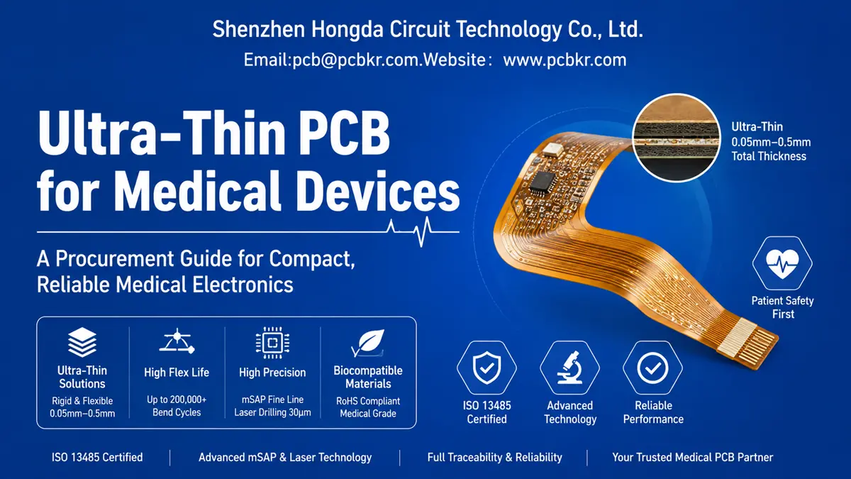
This guide addresses the full ultra thin medical PCB sourcing decision chain—from material qualification and thickness selection to design rules and supplier verification—so that procurement and engineering teams can evaluate a medical flexible PCB partner with evidence rather than assumptions. At Shenzhen Hongda Circuit Technology Co., Ltd., we have produced thin and flexible medical interconnects down to 0.05 mm total thickness, with full mSAP fine-line capability, laser microvia drilling to 30 μm, and ISO 13485-certified process control. The technical parameters and qualification frameworks in this article reflect our actual production floor data.
What Is an Ultra-Thin Medical PCB?
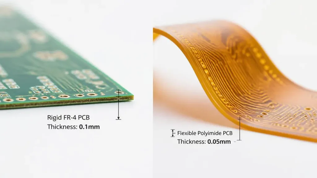
Side-by-side comparison of 0.1mm rigid FR-4 PCB and 0.05mm flexible polyimide PCB
An ultra thin PCB for medical devices is defined less by a single thickness number and more by the structural problem it solves: delivering reliable electrical interconnect in a form factor that conventional rigid boards cannot achieve. In procurement terms, “ultra-thin” spans two distinct material platforms, each with its own qualification gate.
Ultra-Thin Rigid PCB for Medical Applications
The ultra-thin rigid PCB for medical applications category uses standard FR-4 or high-Tg FR-4 laminates pressed to approximately 0.1 mm finished thickness. These boards retain the mechanical stability of glass-reinforced epoxy, which makes them suitable for compact static modules such as portable diagnostic cartridges, pill-camera control boards, and thin-profile patient monitors.
The procurement caveat is critical: a 0.1 mm FR-4 board can survive a single installation bend during assembly, but it is not a medical flexible PCB. If your device specification includes repeated dynamic motion—wearable straps that flex with wrist movement, catheter shafts that articulate through vasculature, or implantable leads that must accommodate cardiac motion—then FR-4, regardless of thickness, is the wrong material choice. At Hongda Circuit, our DFM team flags this distinction during the first review of every thin medical PCB inquiry. We have seen too many programs attempt to save cost by specifying ultra-thin FR-4 for flex applications, only to discover field failures at the 500-cycle mark.
Medical Flexible PCB: Dynamic Bending Solutions
When the device must move, the substrate must move with it. A medical flexible PCB uses polyimide (PI) or liquid crystal polymer (LCP) as the base dielectric, with rolled-annealed copper foil that can withstand repeated bending without work-hardening fracture. Unlike rigid ultra-thin boards, a medical grade flexible circuit board is engineered for fatigue life, not just static thinness.
At our Shenzhen facility, we manufacture single-layer medical flexible PCB constructions down to 0.05 mm total thickness, and multilayer flex builds up to 0.5 mm, with bend-life qualification exceeding 200,000 cycles on select constructions. The shift from FR-4 to PI is not a minor material substitution; it changes every downstream decision—coverlay instead of solder mask, adhesiveless lamination instead of prepreg, and laser direct imaging (LDI) instead of conventional photolithography for trace registration on a moving substrate.
Thickness Options for Medical Devices
Common Thickness Range for Thin Medical PCB
Procurement teams often arrive with a target thickness before they have selected the right material platform. The following table maps realistic thickness ranges to structural categories in thin medical PCB sourcing:
| Construction Type | Typical Thickness Range | Minimum Qualified Thickness (Hongda) | Primary Material |
|---|---|---|---|
| Ultra-thin rigid PCB | 0.1 mm – 0.4 mm | 0.1 mm | FR-4, high-Tg FR-4 |
| Single-layer medical flexible PCB | 0.05 mm – 0.2 mm | 0.05 mm | Polyimide (PI) |
| Double-layer medical flexible PCB | 0.08 mm – 0.3 mm | 0.08 mm | Adhesiveless PI |
| Multilayer medical flexible PCB | 0.15 mm – 0.5 mm | 0.15 mm | PI + coverlay |
| Rigid-flex medical PCB | 0.3 mm – 1.0 mm (total) | 0.3 mm | FR-4 + PI |
The threshold at 0.1 mm is a practical dividing line. Below 0.1 mm, FR-4 becomes mechanically unstable during drilling, plating, and handling; polyimide or LCP becomes mandatory. Our production data shows that ultra thin medical PCB builds below 0.1 mm require roll-to-roll (R2R) processing equipment rather than sheet-based handling, which is why not every supplier claiming “thin PCB capability” can actually produce repeatable 0.05 mm flex circuits at volume.
Thin Construction and Miniaturization Benefits
Thinner substrates deliver three measurable procurement advantages:
- Z-axis space recovery. Every 0.1 mm reduction in board thickness is 0.1 mm of additional battery, sensor, or actuator volume inside the same housing envelope. In hearing aids and continuous glucose monitors, that recovered volume often determines whether the product meets industrial design targets.
- Weight reduction for wearable compliance. A wearable medical PCB that contacts skin for 24-hour wear must minimize mass to prevent adhesive fatigue and patient discomfort. Polyimide flex circuits are up to 70% lighter than equivalent rigid constructions.
- Three-dimensional packaging efficiency. A medical flexible PCB can fold around internal components, run along curved housing walls, or thread through articulating mechanisms. This eliminates connector count, reduces assembly labor, and improves mean time between failures (MTBF) by removing mechanical interconnect points.
Materials Used in Ultra-Thin Medical PCBs
Polyimide Substrate for Medical Flexible PCB
Polyimide remains the dominant substrate for medical flexible PCB production in 2026, and for sound procurement reasons. Kapton-grade PI films offer:
- Thermal stability up to 300°C, surviving reflow and sterilization cycles that would degrade PET or PEN alternatives.
- Chemical resistance to autoclave steam, ethylene oxide, and gamma irradiation—standard sterilization modalities for reusable surgical instruments.
- Low moisture absorption (typically < 1.5% by weight), which prevents delamination and impedance drift in humid clinical environments.
At Hongda Circuit, we stock medical-grade polyimide (IPC-4204/13 compliant) with adhesiveless copper cladding for ultra thin medical PCB builds. The adhesiveless construction eliminates the acrylic or epoxy bond-ply layer found in older flex designs, reducing total thickness by 20–30 μm and eliminating a known delamination path under thermal cycling. For high-frequency wearable applications, we also qualify LCP substrates that offer dielectric constant stability (Dk ~ 2.9) and lower loss tangent than PI above 10 GHz.
FR-4 for Thin Medical PCBs
For static thin medical PCB applications, FR-4 is not obsolete—it is simply misapplied when flex is required. Procurement teams should specify high-Tg FR-4 (Tg ≥ 170°C) when the device will encounter reflow temperatures or sterilization pre-conditioning. Standard Tg 130°C material can survive assembly, but high-Tg laminates reduce the risk of barrel cracking in plated through-holes during thermal shock testing.
Our Shenzhen line produces thin FR-4 medical PCB panels down to 0.1 mm using vacuum lamination and controlled-pressure drilling to prevent fiber breakout. The critical procurement check is this: verify that your supplier has qualified 0.1 mm FR-4 with microsection data showing copper wrap integrity and dielectric thickness uniformity. A supplier who has never shipped 0.1 mm rigid boards in volume will discover handling defects—edge chipping, panel warp, and registration shift—that only appear at scale.
Copper and Surface Finish Selection
Thinner boards require thinner copper, but thinner copper carries less current and is more susceptible to trace fracture under flex. The procurement balance is:
- 1/3 oz (12 μm) copper for single-layer medical flexible PCB where minimum thickness is paramount and current loads are low (sensor interconnects, antenna traces).
- 1/2 oz (18 μm) copper for double-layer flex with moderate power distribution.
- 1 oz (35 μm) copper for rigid-flex constructions where the rigid section carries higher current.
Surface finish selection for biocompatible thin PCB applications must account for both solderability and patient contact safety:
- ENIG (Electroless Nickel Immersion Gold) remains the default for flex assemblies. The gold layer is inert, solderable, and compatible with standard SMT processes. Hongda Circuit qualifies ENIG per IPC-4552B with XRF thickness verification on every lot.
- ENEPIG (Electroless Nickel Electroless Palladium Immersion Gold) eliminates the “black pad” risk associated with high-phosphorus ENIG on fine-pitch components, a consideration for implantable PCB substrate designs with 0.35 mm pitch BGA footprints.
- Hard gold (electrolytic gold over nickel) for edge contacts and connector pads requiring 10,000+ insertion cycles.
- Parylene C coating for implantable or skin-contact devices. This 5–25 μm conformal coating provides a pinhole-free, biocompatible barrier that meets ISO 10993 cytotoxicity requirements.
Medical Device Applications
Wearable Medical PCB Solutions
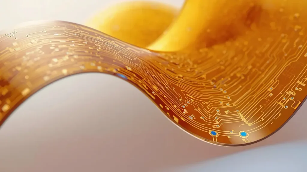
Medical-grade flexible polyimide PCB with mSAP fine lines for wearable devices
The wearable medical device market—continuous glucose monitors, ECG patches, pulse oximetry rings, and smart insulin pens—represents the fastest-growing demand segment for wearable medical PCB interconnects. These devices share three procurement-critical requirements:
- Skin-contact biocompatibility. The medical flexible PCB must pass ISO 10993-5 cytotoxicity and ISO 10993-10 sensitization testing. At Hongda Circuit, we provide material certificates and third-party biocompatibility reports for every medical-grade polyimide lot.
- Sweat and moisture resistance. Wearables encounter perspiration, shower spray, and cleaning agents. Our coverlay-over-copper constructions with ENIG finish have demonstrated 96-hour salt spray resistance per ASTM B117.
- Dynamic flex endurance. A wrist-worn device flexes every time the user types, drives, or exercises. We qualify medical flexible PCB with 100000 bend cycles minimum on standard constructions, with 200,000+ cycles achievable on optimized designs using cross-hatched ground planes and teardrop pad transitions.
Implantable Electronics and Ultra Thin PCB
Implantable devices—pacemakers, neurostimulators, cochlear implants, and emerging bioelectronic interfaces—push ultra thin medical PCB technology to its absolute limit. The procurement stakes are highest here: a failed implantable PCB cannot be serviced without surgery.
For 0.1mm ultra thin PCB for implantable devices, Hongda Circuit produces:
- Single-layer PI flex down to 0.05 mm for capsule endoscopy cameras and temporary cardiac monitors.
- Multilayer rigid-flex with hermetic-seal-compatible plating, where the rigid section carries the ASIC and the flex tail exits through a titanium or ceramic feedthrough.
- mSAP fine-line traces at 30 μm/30 μm line/space, enabling high-density interconnect in footprints smaller than 4 mm × 4 mm.
The critical procurement requirement for implantable applications is hermetic seal compatibility. The PCB must tolerate laser welding or brazing into a titanium housing without outgassing, delamination, or copper oxidation. We pre-qualify all implantable substrate lots for outgassing per ASTM E595 (TML < 1.0%, CVCM < 0.10%).
Minimally Invasive Devices
Surgical endoscopes, arthroscopic shavers, and robotic catheter systems require thin polyimide PCB for endoscopy equipment that can thread through 2 mm instrument channels while carrying image sensor data, LED illumination control, and motor drive signals.
Our rigid-flex thin medical PCB constructions for surgical robotics combine:
- Rigid sections (0.4 mm FR-4) for image sensor and FPGA mounting.
- Flex sections (0.1 mm PI) for articulation joints, with controlled impedance differential pairs for MIPI CSI-2 video at 2.5 Gbps/lane.
- Stiffener integration (polyimide or stainless steel) at connector termination points to prevent flex fatigue at the strain relief boundary.
Diagnostic and Monitoring Equipment
Portable ultrasound probes, point-of-care (POC) diagnostic cartridges, and patient monitoring stations use thin medical PCB technology to reduce device weight and enable battery-powered operation. In these applications, thinness is often secondary to signal integrity: a 0.2 mm multilayer flex carrying 128-channel ultrasound transducer signals requires precise impedance control (±5%) and minimal crosstalk.
Hongda Circuit’s medical flexible PCB capability for diagnostic equipment includes 8-layer flex constructions with stacked microvias, 50 μm laser-drilled blind vias, and controlled impedance to 100 Ω ± 5% on differential pairs. Our LDI (SCREEN Ledia) registration system maintains ±15 μm layer-to-layer alignment, critical for multilayer flex yield.
Key Requirements for Ultra-Thin Medical PCBs
Biocompatibility Standards for Medical Grade Flexible Circuit Board
Every medical grade flexible circuit board that contacts the patient—directly or indirectly—must demonstrate material safety. The procurement team should demand the following evidence gate:
| Test Standard | Purpose | Applicability |
|---|---|---|
| ISO 10993-5 | Cytotoxicity (cell culture) | All patient-contacting devices |
| ISO 10993-10 | Sensitization & irritation | Wearables, skin patches |
| ISO 10993-6 | Implantation (local effects) | Implantable devices |
| USP Class VI | Biological reactivity | FDA-submission support |
| RoHS / REACH | Hazardous substance restriction | All medical electronics |
At Hongda Circuit, our biocompatible thin PCB production operates under ISO 13485:2016 with full material lot traceability. We maintain an approved vendor list (AVL) for polyimide, adhesive, and coating materials with pre-existing biocompatibility test reports. For custom material requests, we coordinate third-party testing through accredited laboratories with 4–6 week turnaround.
Protective Coatings and Encapsulation
The surface of an ultra thin medical PCB must be treated as a potential contamination source until proven otherwise. For implantable and long-term wearable devices, we recommend:
- Parylene C deposition (5–25 μm) for conformal, pinhole-free encapsulation with USP Class VI and ISO 10993 compatibility. Parylene is applied via room-temperature chemical vapor deposition (CVD), which avoids the thermal stress of liquid conformal coatings.
- Low-pressure molding with polyamide hot-melt compounds for wearable sensor modules requiring IP67 ingress protection.
- Hermetic ceramic or metal housings for implantable electronics, with the PCB designed to accommodate laser welding or brazing temperatures without material degradation.
Flex Reliability and Bend Life Testing
A medical flexible PCB with 100000 bend cycles capability is not a marketing claim—it is a test protocol. At Hongda Circuit, we validate flex reliability using IPC-TM-650 2.4.3.1 (Flexural Endurance) with custom fixtures that replicate the actual bend radius and motion profile of the end device.
Key procurement verification points:
- Bend radius validation: We test at the design-specified radius, not a generic 10× thickness proxy. A 0.1 mm flex tested at 1 mm radius behaves differently than the same flex tested at 5 mm radius.
- Dynamic vs. static flex: A “fold-to-ship” flex (static, one-time bend) requires different design rules than a “fold-every-heartbeat” flex (dynamic, 100,000+ cycles).
- Cross-section after cycling: We microsection post-test coupons to detect crack initiation in copper grains, coverlay delamination, or adhesive fatigue.
Traceability and ISO 13485 Manufacturing Control
Medical device regulators and notified bodies do not inspect your supplier’s factory—they inspect your documentation of your supplier’s factory. A qualified ultra thin medical PCB supplier must provide:
- Complete lot traceability: Raw material lot numbers, process parameter logs, inspection records, and test data linked to each finished panel serial number.
- Design History File (DHF) support: Documented evidence that the manufacturing process was validated for the specific device design, including first-article inspection (FAI) reports and process qualification (PQ) data.
- Change control: Formal notification and re-qualification protocols for any material, process, or equipment change that could affect the finished board.
Hongda Circuit’s ISO 13485:2016 quality system includes automated ERP lot tracking, digital work instructions with operator sign-off, and 10-year record retention. For ultra thin medical PCB traceability requirements, we provide Certificate of Conformance (CoC), material certifications, and microsection photographs with every shipment.
Design Considerations for Medical Flexible PCB
Bend Radius Guidelines for Thin Polyimide PCB
The most common design error we correct during DFM review is an unrealistic bend radius. The rule-of-thumb “10× board thickness” is a starting point, not a guarantee. For a thin polyimide PCB in a dynamic application, we recommend:
- Minimum bend radius: 10× total thickness for single-layer flex; 15× for double-layer; 20× for multilayer.
- Keep-out zones: No components, vias, or stiffener transitions within 2 mm of the bend axis.
- Gradual transitions: Use teardrop pads and filleted trace entry angles to reduce stress concentration.
Our engineering team uses finite element analysis (FEA) to model copper strain in the bend region before tooling, identifying high-risk trace geometries before they become field failures.
Trace Routing in Bend Areas
For medical flexible PCB design bend radius guidelines, trace orientation matters more than most designers assume:
- Route traces perpendicular to the bend axis. Traces running parallel to the bend axis experience tensile and compressive strain with every cycle; perpendicular traces experience negligible strain.
- Avoid plated through-holes (PTH) in flex zones. PTH barrels are rigid and will crack under flex. Use blind vias or skip vias that terminate in the rigid section.
- Use cross-hatched ground planes. A solid copper ground plane stiffens the board and creates a “bimetallic strip” curling effect. Cross-hatching at 45° maintains EMI shielding while preserving flexibility.
Layer and Component Placement Optimization
- Minimize layer count. Every additional layer adds thickness, weight, and a potential delamination path. For ultra thin medical PCB designs, we challenge customers to justify every layer.
- Stagger traces layer-to-layer. Do not stack traces vertically in double-sided flex that will fold. Staggering distributes mechanical stress and prevents the “I-beam” fracture mode.
- Place heavy components on rigid islands. BGAs, connectors, and batteries belong on rigid sections with stiffener support, never on the flex tail.
Ultra-Thin Rigid PCB vs. Medical Flexible PCB
| Evaluation Criteria | Ultra-Thin Rigid PCB | Medical Flexible PCB |
|---|---|---|
| Primary Material | FR-4, high-Tg FR-4 | Polyimide (PI), LCP |
| Typical Thickness | 0.1 mm – 0.4 mm | 0.05 mm – 0.5 mm |
| Bend Capability | Single static bend only | 100,000+ dynamic cycles |
| Design Focus | Structural stability, warp control | Bend radius, fatigue life, trace routing |
| Surface Finish | ENIG, OSP, immersion tin | ENIG, ENEPIG, hard gold, Parylene C |
| Key Applications | Diagnostic cartridges, pill cameras, thin monitors | Wearables, implants, surgical robotics, catheters |
| Manufacturing Risk | Handling damage, edge chipping | Dimensional shift, coverlay delamination |
| Cost Driver | Thin-core material yield | Layer count, bend testing, biocompatibility docs |
The ultra thin rigid PCB vs medical flexible PCB comparison is not about which is “better.” It is about matching the material platform to the mechanical requirement. Our DFM team at Hongda Circuit reviews every medical inquiry to confirm this match before quoting, because a mis-specified substrate is the most expensive mistake a procurement team can make.
Why Choose an Ultra-Thin PCB for Medical Devices?
The decision to specify an ultra thin PCB for medical devices is driven by five procurement-validated benefits:
- Space recovery in constrained housings. A 0.1 mm rigid board or 0.05 mm flex circuit reclaims Z-axis volume for batteries, sensors, or thermal management.
- Weight reduction for patient compliance. Wearable and implantable devices must minimize mass to prevent adhesive failure, tissue irritation, or patient non-compliance.
- Connector elimination through flex integration. A medical flexible PCB can replace wire harnesses and board-to-board connectors, reducing BOM cost, assembly labor, and failure points.
- Improved thermal and electrical performance. Flat copper conductors in flex designs dissipate heat more effectively than round wire, and shorter interconnect paths reduce parasitic inductance.
- Three-dimensional packaging freedom. Flex circuits fold around mechanical structures, enabling product geometries that rigid boards cannot achieve.
At Shenzhen Hongda Circuit Technology Co., Ltd., we support these benefits with manufacturing infrastructure specifically configured for thin medical PCB production: SCREEN Ledia LDI for ±15 μm registration on flex substrates, Mitsubishi UV/CO₂ hybrid laser drilling for 30 μm microvias, LAUFFER vacuum lamination for thin-core FR-4, and Nordson DAGE X-ray for void detection in copper-filled vias. Our ISO 13485:2016 and IPC-6012 Class 3/3A certifications provide the quality system foundation that medical procurement teams require for supplier qualification.
Manufacturing and Quality Considerations
Sourcing an ultra thin medical PCB supplier requires verification beyond capability lists. The following checklist reflects the actual qualification gates we recommend to medical OEMs evaluating Hongda Circuit or any competitor:
| Verification Item | What to Demand | Hongda Circuit Evidence |
|---|---|---|
| Material lot traceability | ERP-linked lot numbers from raw material to finished board | Full ERP traceability with 10-year retention |
| Microvia capability | Production data on minimum via diameter, aspect ratio, and stacked vs. staggered yield | 30 μm UV laser, 20 μm femtosecond; 2.5M microvias/day |
| Fine-line capability | Documented line/space with yield data | mSAP at 30 μm/30 μm; 8 μm/8 μm for advanced interposers |
| Biocompatibility | ISO 10993 test reports for substrate, adhesive, and coating | Pre-qualified PI lots; third-party testing coordination |
| Bend life validation | IPC-TM-650 test reports at design-specific radius | Custom flex endurance testing to 200,000+ cycles |
| Impedance control | Statistical process control (SPC) data for Zo tolerance | ±5% on differential pairs; 2.5D field solver validation |
| Cleanroom assembly | ISO 14644 Class 7 or better for implantable devices | Class 7 cleanroom for medical assembly operations |
| Fast prototype turnaround | Lead time for first articles without capacity queue | 48-hour for standard HDI; 5-day for 10–16 layer builds |
Critical procurement caution: Do not select a supplier based on quoted unit price alone for thin medical PCB with ISO 13485 certification. The total cost of ownership includes yield loss, field failure liability, regulatory submission delays, and redesign cycles. A 15% higher unit price from a supplier with verified mSAP capability, full traceability, and documented bend-life data is almost always lower TCO than a commodity quote from a generalist fabricator.
Conclusion: Making the Right Thin Medical PCB Decision
The ultra thin PCB for medical devices market in 2026 offers more material options, finer feature capabilities, and denser interconnect technologies than ever before. For procurement teams, this abundance creates a paradox: more suppliers claim capability, but fewer can prove it through documented process control, certified quality systems, and transparent production data.
For static, compact structures, the thin medical PCB path through ultra-thin FR-4 remains viable and cost-effective. For devices that bend, flex, or implant, the medical flexible PCB route through polyimide or LCP is non-negotiable. The wrong choice between these platforms is not a manufacturing inconvenience—it is a product failure mode.
At Shenzhen Hongda Circuit Technology Co., Ltd., we have structured our medical PCB program around evidence-based qualification, not marketing claims. Our ISO 13485:2016 system, mSAP fine-line production, laser microvia infrastructure, and documented flex reliability testing provide the technical foundation that medical device procurement teams need to de-risk their supply chain.
Ready to evaluate your ultra thin medical PCB project?
Submit your Gerber files, stack-up requirements, and device application details to sales@pcbkr.com. Our engineering team will return a complimentary DFM review, material recommendation, and detailed quotation within 24 hours.
Shenzhen Hongda Circuit Technology Co., Ltd.
📧 Sales: sales@pcbkr.com
📧 Engineering: pcb@pcbkr.com
📞 Phone: +86 0755 23720053
🌐 Website: www.pcbkr.com
📍 Address: Room 1608-1610, Research Development Comprehensive Building, Baoyunda Logistics Center, Baoan, Shenzhen, China
🏢 Certifications: ISO 9001:2015 | ISO 13485:2016 | IPC-6012 Class 3/3A | IATF 16949 | AS9100D
Frequently Asked Questions: Ultra-Thin Medical PCB Procurement
How do I verify that a supplier can actually produce 0.1 mm ultra-thin rigid PCBs for medical devices, not just quote them?
Demand three pieces of evidence: (1) a microsection photograph of a production 0.1 mm board showing copper wrap, dielectric thickness, and layer registration; (2) process capability data (CpK) for thickness control across a production panel; and (3) references from at least two medical OEMs who have received volume shipments. At Hongda Circuit, we provide all three during the qualification phase, along with IPC-6012 Class 3 inspection reports,
What is the real difference in bend life between a 0.1 mm FR-4 board and a 0.1 mm polyimide medical flexible PCB?
A 0.1 mm FR-4 board may survive a single 90-degree installation bend. A 0.1 mm polyimide medical flexible PCB, properly designed with cross-hatched ground planes and teardrop pads, can exceed 100,000 dynamic bend cycles at a 5 mm radius. The difference is not incremental—it is three orders of magnitude. If your device specification includes any repeated motion, FR-4 is the wrong material, regardless of thickness.
For implantable devices, what surface finish and coating combination do you recommend?
For implantable ultra thin medical PCB applications, we recommend ENEPIG (to eliminate black pad risk on fine-pitch components) followed by Parylene C conformal coating at 10–15 μm. ENEPIG provides a solderable, wire-bondable surface; Parylene C provides a biocompatible, pinhole-free moisture barrier that meets ISO 10993-5 cytotoxicity requirements. For hermetic packages, the PCB must also be qualified for outgassing per ASTM E595.
How does Hongda Circuit handle lot traceability for medical flexible PCBs under ISO 13485?
Every medical flexible PCB lot is tracked through our ERP from raw material receipt (polyimide roll number, copper foil lot, adhesive batch) through every process step (etching, drilling, plating, lamination, inspection) to finished panel serial numbers. We retain material certificates, process parameter logs, AOI/X-ray images, and electrical test data for 10 years. This documentation package supports your Design History File (DHF) and regulatory submission requirements without additional fees.
What lead time should I expect for a medical flexible PCB prototype, and how does it differ from mass production?
For thin medical PCB prototype orders, Hongda Circuit offers 48-hour turnaround for single-layer flex with standard materials in stock, and 5–7 days for multilayer rigid-flex with impedance control and microvias. Mass production lead times range from 2–3 weeks for single-layer flex to 4–6 weeks for complex rigid-flex with sequential lamination. The critical procurement note: prototype and production must use the same material lot and process parameters to ensure qualification transfer. We lock the process flow at prototype approval to prevent “prototype hero, production zero” syndrome.
About Author
David Chen https://www.linkedin.com/in/pcbcoming
David Chen boasts an extensive professional background in PCBA manufacturing, PCBA testing, and PCBA optimization, with specialized expertise in high-precision PCBA fault analysis and rigorous PCBA reliability testing. The author has worked with high-layer-count server PCB fabrication, ultra-low-loss backplane stackups, and thermo-mechanical reliability optimization for AI infrastructure projects involving 112G and 224G PAM4 architectures. Skilled in complex circuit design and cutting-edge advanced PCB manufacturing processes, he delivers solutions that elevate product durability and performance across industrial applications. His technical articles focusing on PCBA manufacturing workflows and testing methodologies are widely cited by industry peers, research institutions, and technical platforms, solidifying his reputation as a recognized technical authority in the global circuit board manufacturing sector.