Ethernet Switch PCB: Manufacturing, Assembly, Testing, and Supplier Selection
An Ethernet switch PCB connects switching controllers, Ethernet PHYs, network ports, power circuits, and management interfaces in wired networking equipment. Successful manufacturing requires the right layer stackup, suitable laminate materials, controlled impedance where specified, reliable PCB assembly, and appropriate electrical testing. For OEM buyers, supplier selection should be based on design requirements, manufacturing feasibility, quality documentation, and total project cost—not price alone.
This guide explains how to evaluate Ethernet switch PCB fabrication and assembly, identify critical engineering risks, prepare an RFQ, and qualify a manufacturing partner from prototype through production.
What Is an Ethernet Switch PCB and Which Applications Use It?
An Ethernet switch PCB is a printed circuit board that supports the electrical connections and components required to receive, process, and forward Ethernet traffic. Depending on the product architecture, it may contain switching controllers, Ethernet physical-layer transceivers, magnetics interfaces, RJ45 or SFP-family connectors, power management circuits, and system management components.
Different applications impose different requirements on PCB design and manufacturing.
| Application | Typical PCB priorities | Key manufacturing considerations |
|---|---|---|
| Industrial Ethernet switch | Reliability, noise immunity, environmental durability | Material selection, grounding, thermal management, inspection |
| Enterprise network switch | Port density, signal integrity, stable power delivery | Multilayer construction, impedance control, connector placement |
| PoE Ethernet switch | Power delivery, heat dissipation, port protection | Copper sizing, current paths, thermal design, assembly quality |
| Managed Ethernet switch | Switching performance, control interfaces, serviceability | Component integration, routing density, functional testing |
| Rugged or outdoor switch | Environmental resistance and mechanical reliability | Suitable materials, protective measures, enclosure compatibility |
| Data center switch | High-speed signaling, dense routing, demanding power requirements | Low-loss materials, advanced stackup engineering, electrical verification |
For more demanding networking applications, see our guide to data center switch PCB manufacturing, which focuses on high-speed switching architectures, low-loss materials, and supplier qualification.
The appropriate manufacturing process depends on the actual board design. An industrial switch with moderate-speed interfaces may prioritize robustness and cost, while a high-bandwidth switch may require more demanding electrical performance and fabrication controls.
How Do Ethernet Speed, Port Count, and Architecture Affect PCB Requirements?
Ethernet speed and port count influence routing density, connector placement, power consumption, thermal design, and manufacturing complexity. However, the required PCB construction cannot be determined from the advertised aggregate switching capacity alone.
How Does Ethernet Speed Influence PCB Design?
Different Ethernet interfaces impose different signaling, routing, and channel requirements. The relevant specifications depend on the physical interface, lane configuration, component selection, and system architecture.
Before approving a stackup, the engineering team should establish:
- Ethernet interface types and supported data rates.
- Switching controller and PHY requirements.
- Number and location of high-speed signal channels.
- Connector types and transmission-path lengths.
- Impedance targets and applicable tolerances.
- Channel insertion-loss requirements, where specified.
- Power consumption and cooling constraints.
A higher aggregate network capacity does not automatically determine the number of PCB layers or the laminate grade. These decisions require review of the actual electrical design.
Does a Higher Port Count Require More PCB Layers?
A higher port count can increase routing density and component-placement constraints, but layer count also depends on the controller package, board dimensions, routing topology, power distribution, and grounding strategy.
A larger board with a less dense component layout may be easier to route than a smaller board with fine-pitch packages and complex high-speed interfaces.
The manufacturer should review the PCB layout, proposed stackup, copper distribution, via structure, and mechanical constraints before recommending a layer count. This helps avoid unnecessary fabrication complexity and cost.
Which PCB Materials and Stackup Options Are Suitable for Ethernet Switches?
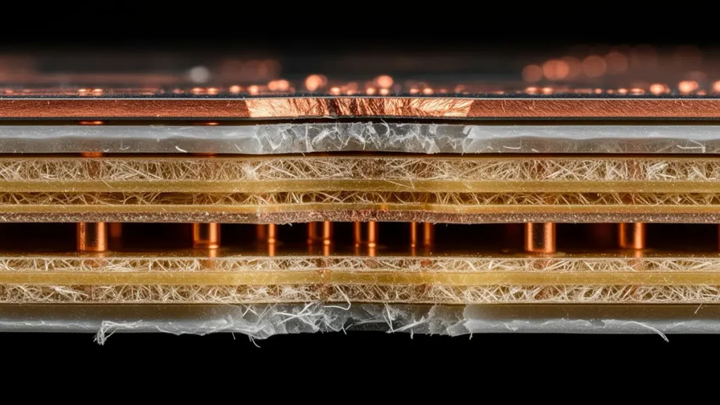
Ethernet Switch PCB multilayer stackup showing copper layers, dielectric materials, and ground planes
The best Ethernet switch PCB material is the material system that meets the design’s electrical, thermal, mechanical, and reliability requirements at an acceptable cost.
FR-4 may be appropriate for many industrial and enterprise switch designs. More demanding high-speed channels may require lower-loss laminate systems, depending on the channel budget and operating frequency.
When Is Standard FR-4 Suitable?
Standard FR-4 can be a practical choice when its electrical characteristics, thermal properties, and manufacturing tolerances satisfy the design requirements.
Material selection should consider:
- Dielectric constant (Dk) and dissipation factor (Df).
- Finished board thickness and dielectric spacing.
- Copper thickness and conductor geometry.
- Glass construction and copper roughness.
- Thermal requirements and assembly process compatibility.
- Availability, traceability, and total material cost.
The material grade should be specified rather than identified only by the generic term “FR-4.” Different grades and constructions can produce different electrical and manufacturing results.
When Should Buyers Consider Low-Loss PCB Materials?
Low-loss materials may be appropriate when high-speed channels have limited insertion-loss budgets or operate at frequencies where dielectric and conductor losses become significant.
A material decision should be based on the entire channel, including PCB traces, vias, connectors, packages, and other interconnects. Selecting a laminate with a lower published Df does not, by itself, guarantee that the assembled system will meet its electrical target.
For complex networking boards, the PCB manufacturer should review the material grade, stackup, dielectric thickness, copper type, and manufacturing tolerances before quotation.
How Does Ethernet Switch PCB Manufacturing Control Signal Integrity?
Ethernet switch PCB manufacturing affects signal integrity through trace geometry, dielectric thickness, copper roughness, layer registration, via transitions, and reference-plane continuity. These factors should be considered together with the electrical requirements of the finished design.
Why Are Controlled Impedance and Reference Planes Important?
Controlled impedance helps manage reflections caused by discontinuities along transmission paths. A continuous and appropriately designed reference plane also supports predictable return-current paths and reduces unwanted coupling.
Many high-speed interfaces use nominal differential impedance targets such as 100 ohms, but the correct target must come from the relevant interface and system specifications.
The fabrication documentation should identify:
- Controlled signal layers and structures.
- Target impedance and acceptable tolerance.
- Stackup and dielectric construction.
- Required reference planes.
- Test-coupon design and measurement method.
- Required impedance report and acceptance criteria.
Trace width alone is not a complete impedance specification. The surrounding dielectric, copper thickness, spacing, and reference-plane arrangement all affect the finished transmission-line characteristics.
For additional guidance on stackup engineering and high-speed routing, read our high-speed PCB manufacturing guide.
When Is Via Backdrilling Necessary?
Backdrilling removes unused portions of plated through-hole vias that may behave as electrical stubs. Depending on the signaling requirements and via geometry, these stubs can contribute to reflections and resonances.
Backdrilling should be considered when channel analysis indicates that residual via stubs compromise the electrical budget. It is not automatically required for every Ethernet switch PCB.
Before production, the buyer and fabricator should confirm the affected vias, drilling direction, target depth, acceptable residual-stub length, and inspection requirements.
How Should Impedance Be Tested and Documented?
Time-domain reflectometry (TDR) is commonly used to evaluate impedance behavior along a transmission path or test structure. A vector network analyzer (VNA) can measure frequency-dependent parameters such as insertion loss and return loss when the appropriate setup and calibration are used.
These tests provide different information. A TDR report alone does not prove that insertion loss meets a specified frequency-dependent limit.
For procurement, buyers should define the required measurement, test frequency range where applicable, acceptance criteria, test structure, reporting format, and sampling plan.
See our impedance-controlled PCB manufacturing guide for further information on impedance specifications, fabrication controls, and verification.
How Can Ethernet Switch PCB Manufacturers Manage Power and Thermal Risks?
Power delivery and thermal performance are particularly important in PoE equipment, high-port-count switches, and systems containing power-hungry switching components.
The design must provide suitable current paths, manage voltage drop, control heat, and maintain reliability under the expected operating conditions.
How Does PoE Affect PCB Manufacturing Requirements?
Power over Ethernet designs deliver power through designated network connections in addition to transmitting data. The PCB must support the specified current paths and power-management architecture while maintaining appropriate insulation, spacing, and thermal performance.
The design review should address:
- Maximum current and voltage requirements.
- Copper thickness and conductor dimensions.
- Power-path resistance and voltage-drop limits.
- Connector and component current ratings.
- Thermal rise and enclosure cooling.
- Protection circuits and relevant safety requirements.
Increasing copper thickness may reduce conductor resistance, but it can also affect etching, spacing, finished geometry, and fabrication cost. Copper specifications should therefore follow the electrical and thermal design rather than a generic preference for heavier copper.
How Can PCB Design Reduce Heat-Related Reliability Risks?
Thermal performance depends on component losses, copper distribution, board geometry, thermal vias, mounting conditions, and the cooling system.
Manufacturing feasibility should be reviewed alongside the system thermal design. For example, thermal vias may improve heat transfer in a suitable layout, but their effectiveness depends on placement, construction, and the available path to a heat sink or other cooling structure.
The buyer should provide relevant temperature limits, power dissipation data, enclosure constraints, and any required thermal qualification criteria.
What Should Buyers Know About Ethernet Switch PCB Assembly?
Ethernet switch PCB assembly combines component sourcing, solder-paste printing, component placement, soldering, inspection, and testing to produce a populated board. The appropriate scope depends on whether the buyer needs bare PCB fabrication, assembled PCBs, or a turnkey manufacturing service.
For projects requiring component sourcing and board assembly in addition to bare-board fabrication, explore our PCB assembly services.
Which Assembly Processes Are Commonly Required?
The assembly process depends on the bill of materials (BOM), package types, component pitch, board dimensions, and production volume. A typical surface-mount assembly workflow may include:
- BOM and component-package review.
- Component availability and approved-substitute checks.
- Solder-paste printing.
- Pick-and-place operations.
- Reflow soldering.
- Automated optical inspection (AOI).
- X-ray inspection where appropriate.
- Electrical or functional testing according to the project requirements.
Through-hole connectors or other mechanically demanding components may require additional soldering and inspection operations.
The manufacturing plan should account for fine-pitch packages, connector alignment, component thermal requirements, and the accessibility of test points.
What Information Is Needed Before Assembly Quotation?
To prepare an accurate PCBA quotation, buyers should provide:
- Complete BOM with manufacturer part numbers.
- Gerber, ODB++, or other agreed manufacturing data.
- Assembly drawings and component-placement files.
- PCB thickness, copper, and surface-finish requirements.
- Approved component alternatives, if any.
- Expected prototype and production quantities.
- Testing, packaging, and traceability requirements.
Missing or ambiguous component information can delay sourcing and make quotations difficult to compare. Any substitution should be approved through an agreed engineering or procurement process.
Which Quality Tests and Documents Should an Ethernet Switch PCB Supplier Provide?
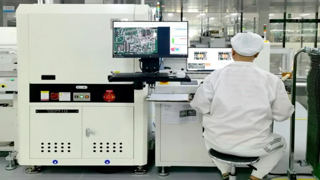
Ethernet Switch PCB quality inspection using AOI and electrical testing equipment
The required quality plan depends on product complexity, electrical performance targets, applicable standards, and the buyer’s acceptance requirements. Buyers should define the verification scope before production rather than assume that every supplier includes the same tests.
| Verification item | Purpose | What buyers should request |
|---|---|---|
| Electrical continuity and isolation | Detect opens and unintended shorts | Test coverage and results |
| Impedance testing | Verify specified transmission-line structures | Target values, tolerances, and TDR report |
| AOI | Identify visible fabrication or assembly defects | Inspection criteria and relevant records |
| X-ray inspection | Examine hidden solder joints or internal features where applicable | Inspection scope and acceptance criteria |
| Microsection analysis | Examine internal construction and plated structures | Cross-section records when required |
| Dimensional inspection | Verify thickness, outline, and critical dimensions | Measurement records |
| Functional testing | Check specified board-level functions | Test procedure and pass/fail criteria |
| Material traceability | Support quality investigations and revision control | Material identification and applicable records |
Not every test is necessary for every product, and not every test is performed on every production lot. The inspection and test plan should specify which tests apply to prototypes, qualification builds, and routine production.
Where the project requires regulatory or industry-specific compliance, the buyer should identify the applicable standards and documentation requirements in the purchase specification.
What Determines Ethernet Switch PCB Manufacturing Cost and Lead Time?
Ethernet switch PCB cost and lead time depend on the manufacturing specification, material availability, design complexity, order quantity, component sourcing, inspection scope, and production schedule.
Which Factors Have the Greatest Impact on PCB Fabrication Cost?
Important cost drivers include:
- Layer count and finished board dimensions.
- Laminate type and availability.
- Copper thickness and special processing requirements.
- Controlled-impedance structures and tolerances.
- Blind, buried, or other specialized via structures.
- Backdrilling, if required.
- Surface finish and dimensional tolerances.
- Electrical testing and documentation.
- Order quantity and panel utilization.
A more complex specification may increase processing time and reduce manufacturing yield if critical parameters are difficult to control. Early design-for-manufacturing (DFM) review can identify avoidable costs before the design is released.
What Affects PCBA Cost and Delivery Time?
For assembled boards, additional factors include component lead times, BOM availability, package complexity, sourcing restrictions, stencil requirements, inspection scope, and functional test development.
Long-lead or obsolete components can delay a project even when the bare PCB can be fabricated quickly. Buyers should identify approved alternatives early and confirm whether substitutions require engineering validation.
A reliable quotation should separate relevant cost categories where practical and identify assumptions about material availability, component sourcing, testing, and delivery.
How Can Buyers Reduce Cost Without Compromising Reliability?
Useful measures include simplifying the stackup where the electrical design permits, avoiding unnecessary specialized vias, standardizing materials where appropriate, resolving DFM issues early, and agreeing on the inspection plan before production.
Cost reduction should not depend on unapproved material substitutions, relaxed critical tolerances, or removal of required tests. Any proposed change should be assessed against the product’s electrical, mechanical, and reliability requirements.
How Should OEM Buyers Evaluate an Ethernet Switch PCB Manufacturer?
A qualified supplier should demonstrate that its manufacturing processes, materials, quality controls, and testing capabilities match the actual board specification.
Buyers should evaluate documented capability rather than rely solely on general claims about advanced equipment or maximum layer count.
Which Manufacturing Capabilities Should Buyers Verify?
The supplier review should cover:
- Supported layer counts, board dimensions, and thickness ranges.
- Available laminate grades and material traceability.
- Copper thickness and via structures.
- Controlled-impedance capability and measurement methods.
- Relevant drilling, registration, and lamination tolerances.
- Assembly capability for the required component packages.
- Inspection and testing available for the project.
- Process-change controls and production traceability.
The buyer should also establish whether prototype, pilot, and volume production can maintain the approved design and acceptance criteria.
What Questions Should Buyers Ask Before Placing an Order?
Before awarding a project, ask the supplier to clarify:
- Which specification items require additional engineering review?
- Which materials and fabrication processes are proposed?
- Which electrical and dimensional tests are included?
- What quality records will accompany the shipment?
- How will component substitutions and material changes be controlled?
- How will defects, nonconformances, and corrective actions be managed?
- Which quotation assumptions could affect cost or lead time?
Answers should be specific to the project and documented in the quotation, manufacturing specification, quality agreement, or purchase order as appropriate.
What Information Should Buyers Include in an Ethernet Switch PCB RFQ?
A complete request for quotation (RFQ) gives the manufacturer enough information to evaluate feasibility, estimate production effort, identify risks, and provide a meaningful price and delivery proposal.
| RFQ category | Recommended information |
|---|---|
| Application | Industrial, enterprise, PoE, rugged, or data center switch |
| Manufacturing scope | Bare PCB, PCBA, or turnkey sourcing and assembly |
| Design files | Gerber, ODB++, IPC-2581, or agreed formats |
| Stackup | Layer count, material grade, dielectric thickness, copper weight |
| Electrical requirements | Impedance targets, tolerances, interface specifications |
| Mechanical requirements | Dimensions, thickness, tolerances, connector constraints |
| Via requirements | Through, blind, buried, or backdrilled structures |
| Surface finish | Required finish and acceptance criteria |
| BOM and assembly data | Part numbers, placement files, assembly drawings |
| Quantity | Prototype, pilot, and forecast production quantities |
| Quality requirements | Inspection, electrical testing, traceability, qualification |
| Delivery | Target date, shipping destination, and production milestones |
If some details are not finalized, identify them as open engineering items. A supplier can then distinguish the information needed for an initial quotation from the items that must be resolved before production.
How Can Shenzhen Hongda Circuit Technology Support Ethernet Switch PCB Projects?
Shenzhen Hongda Circuit Technology Co., Ltd. supports PCB manufacturing and PCBA assembly projects that require engineering review, manufacturing planning, and defined quality requirements.
For an Ethernet switch project, the first step is to review the actual design data, stackup, material requirements, electrical specifications, production quantity, and testing expectations. The appropriate process and delivery plan should be confirmed against the specific project rather than assumed from a general capability statement.
What Should Buyers Prepare for an Engineering Review?
Prepare the latest PCB fabrication files, stackup details, BOM if assembly is required, controlled-impedance specifications, mechanical requirements, target quantity, and desired delivery date.
If the project requires impedance reports, specialized electrical measurements, X-ray inspection, functional testing, or particular quality documents, include those requirements in the RFQ.
How Can Buyers Request an Ethernet Switch PCB Quote?
Send your design files and procurement requirements to Shenzhen Hongda Circuit Technology Co., Ltd. for a manufacturing review and quotation.
- Company: Shenzhen Hongda Circuit Technology Co., Ltd.
- Website: https://www.pcbkr.com/
- Email: pcb@pcbkr.com
Request an Ethernet Switch PCB Manufacturing and Assembly Review to clarify fabrication feasibility, assembly scope, quality requirements, and production planning.
Frequently Asked Questions About Ethernet Switch PCBs
What Is an Ethernet Switch PCB?
An Ethernet switch PCB is a printed circuit board used in wired networking equipment to connect switching controllers, PHYs, network interfaces, power circuits, and management components.
Which PCB Material Is Best for an Ethernet Switch?
The appropriate material depends on signaling requirements, operating frequency, thermal conditions, mechanical constraints, and cost. FR-4 may suit many designs, while demanding high-speed channels may require lower-loss laminates.
How Many Layers Does an Ethernet Switch PCB Need?
Layer count depends on routing density, component packages, board dimensions, power distribution, grounding, and signal-integrity requirements. The final stackup should be established through design review and manufacturing assessment.
Does an Ethernet Switch PCB Need Controlled Impedance?
Controlled impedance is required when specified by the electrical interfaces and signal-channel design. The target values, tolerances, controlled structures, and verification method should be documented in the fabrication package.
When Is Backdrilling Required for an Ethernet Switch PCB?
Backdrilling may be required when unused via stubs cause unacceptable electrical discontinuities. The need depends on the channel design, via geometry, and applicable signal-integrity limits.
What Tests Should Buyers Request from an Ethernet Switch PCB Manufacturer?
Depending on the design, relevant tests may include continuity and isolation, impedance measurement, dimensional inspection, microsection analysis, AOI, X-ray inspection, and functional testing. The required scope should be agreed upon before production.
Can the Same Supplier Manufacture and Assemble an Ethernet Switch PCB?
Yes. A supplier offering both PCB fabrication and PCBA services may coordinate bare-board manufacturing, component sourcing, assembly, inspection, and agreed testing. Buyers should confirm the actual service scope and responsibilities.
What Determines Ethernet Switch PCBA Cost?
Cost depends on the bare PCB specification, component prices and availability, assembly complexity, production quantity, inspection and testing requirements, and delivery schedule.
What Files Are Required for an Ethernet Switch PCB Quote?
Typical files include Gerber or ODB++ data, stackup specifications, fabrication drawings, and quantity requirements. For PCBA, provide the BOM, component-placement data, assembly drawings, and any test requirements.
How Can OEM Buyers Qualify an Ethernet Switch PCB Supplier?
Evaluate process capability, material traceability, impedance verification where applicable, inspection methods, quality documentation, change control, and the supplier’s ability to meet the approved specification from prototype through production.
How Can I Request an Ethernet Switch PCB Manufacturing Quote?
Contact Shenzhen Hongda Circuit Technology Co., Ltd. at pcb@pcbkr.com or visit https://www.pcbkr.com/. Include your design files, material and stackup requirements, order quantity, assembly scope, testing requirements, and target delivery date.
About the Author
David Chen is a senior PCB manufacturing engineer at Shenzhen Hongda Circuit Technology Co., Ltd. His technical focus includes PCB fabrication, PCBA manufacturing and testing, process optimization, fault analysis, reliability, and advanced PCB manufacturing.
LinkedIn: David chen