Ultra-Thin PCB for Wearable Electronics: A Procurement Engineer’s Guide to Sourcing Reliable Wearable Flexible PCB Solutions
When procurement teams source an ultra thin PCB for wearable devices, the gap between a supplier’s marketing claims and actual factory capability can cost an OEM six months in delayed launches. Wearable electronics—smartwatches, health monitoring bands, AR/VR headsets—demand circuit boards that are not merely thin, but mechanically reliable under repeated flexing, thermally stable across skin-temperature ranges, and manufacturable at scale without the warpage or delamination that destroys yield.
This guide is written for buyers, hardware project managers, and supply chain engineers who need to move beyond datasheets and verify real manufacturing capability. We cover the technical specifications that matter, the material choices that determine field reliability, and the 2026 process technologies that separate qualified wearable ultra thin PCB manufacturers from trading companies that outsource to third-tier fabs.
What Is an Ultra Thin PCB for Wearable Devices? Understanding the Technology Behind Modern Wearable Electronics
Defining Ultra-Thin Standards: From 0.05 mm Flex to 0.8 mm Rigid-Flex for Wearable Applications
An ultra thin PCB for wearable electronics is not simply a standard board milled down. In production terminology, it refers to printed circuit boards with a total finished thickness of 0.05 mm to 0.2 mm for single-layer or multilayer flexible constructions, and up to 0.8 mm for rigid-flex assemblies that integrate both rigid component mounting zones and dynamic flex sections.
For procurement teams, the critical distinction lies in how that thinness is achieved. A 0.1 mm flexible PCB built with standard adhesive-based polyimide will delaminate after 3,000 bending cycles. The same thickness built with adhesiveless thermoplastic polyimide (TPI) and processed through vacuum lamination can survive 100,000+ dynamic flex cycles with resistance change under 10%. The material stack-up and lamination protocol matter more than the thickness number on paper.
At Shenzhen Hongda Circuit Technology, our wearable flexible PCB production line handles single-layer flex down to 50 µm total thickness and rigid-flex wearable assemblies at 0.1–0.15 mm in the flex region, with rigid sections engineered to IPC-6013 Class 3 reliability standards.
Why Wearable Ultra Thin PCB Technology Is Non-Negotiable for Smartwatch and Health Monitor OEMs
The shift from “technology push” to “procurement pull” in wearable electronics is driven by three irreversible market forces:
- Space constraint: A premium smartwatch has less than 8 mm of internal z-axis height. The motherboard, battery, haptic motor, and sensor array must coexist without interference. A thin PCB for smartwatch integration is the only architecture that leaves room for a meaningful battery cell.
- Biomechanical conformity: Health monitoring wearables must maintain skin contact. Rigid boards create pressure points and break seals. Wearable flexible PCB solutions conform to wrist curvature and move with the body without solder joint fatigue.
- Signal integrity at density: Modern wearables integrate Bluetooth 5.3, NFC, and multi-channel biometric sensors. HDI microvia technology on ultra-thin substrates enables 90Ω controlled differential pairs for antenna routing in a footprint that subtractive etching cannot achieve.
Thin PCB for Smartwatch and Health Wearables: Critical Specifications Buyers Must Verify Before Placing Orders
Procurement’s most expensive mistake is assuming that any flex PCB supplier can reliably produce 0.1 mm boards with HDI features. Before issuing a PO, verify these five capability gates:
Thickness Tolerance and Material Stack-Up Requirements for Wearable Flexible PCB
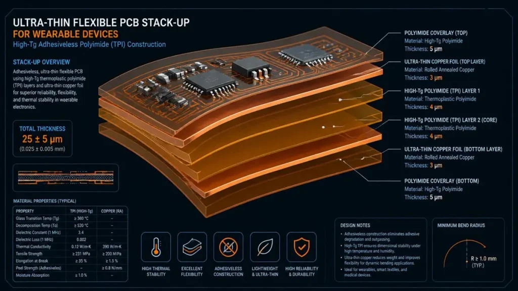
Ultra-Thin Flexible PCB Stack-Up Diagram (Adhesiveless TPI Construction)
| Parameter | Typical Capability | Wearable-Grade Requirement | Why It Matters for Buyers |
|---|---|---|---|
| Total Thickness | 0.1–0.6 mm | 0.05–0.2 mm flex; 0.8 mm rigid-flex | Determines enclosure fit and battery volume |
| Base Material | Standard PI with adhesive | Adhesiveless TPI or high-Tg PI (≥170°C) | Adhesive layers crack under thermal cycling and repeated bending |
| Copper Weight | 1 oz (35 µm) | 3–12 µm (ultra-thin foil) | Thinner copper enables finer lines and reduces stress on flex regions |
| Coverlay | Liquid photoimageable solder mask | Polyimide coverlay | Solder mask cracks when bent; coverlay maintains peel strength ≥ 0.7 N/mm |
Buyer action item: Request a cross-sectional photograph of the supplier’s actual 0.1 mm production sample. If they cannot provide it, they have not solved the handling and etching challenges of ultra-thin material.
HDI Microvia and Any-Layer Interconnect Capabilities in Wearable Ultra Thin PCB
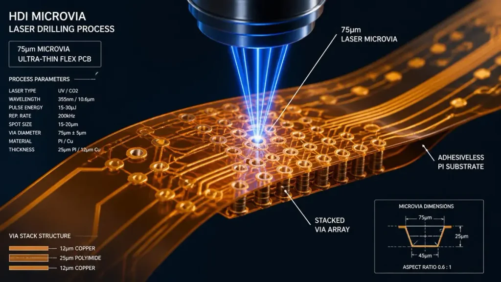
Technical 3D render of HDI microvia laser drilling process (75µm microvia, adhesiveless PI substrate) by Shenzhen Hongda Circuit Technology Co., Ltd
Wearable devices route signals between sensors, MCUs, and wireless modules in three dimensions. This demands laser-drilled microvias with diameters down to 75 µm and any-layer HDI interconnect density.
Traditional through-hole drilling is impossible below 0.2 mm board thickness without destroying the substrate. Only suppliers with UV/CO₂ laser drilling systems can place blind and buried microvias in ultra-thin build-up dielectrics. At Hongda Circuit, our Mitsubishi Electric UV/CO₂ laser drilling platform achieves 50–75 µm microvia diameters in 25 µm PI films, with positional accuracy suitable for stacked via structures up to four layers deep.
Red flag for procurement: If a supplier quotes 0.1 mm boards but only offers mechanical drilling with 0.15 mm minimum holes, they will route traces around vias instead of through them—consuming 30–40% more board area and forcing larger product dimensions.
Dynamic Flexing Reliability: IPC-6013 Class 3 Standards Every Procurement Team Should Demand
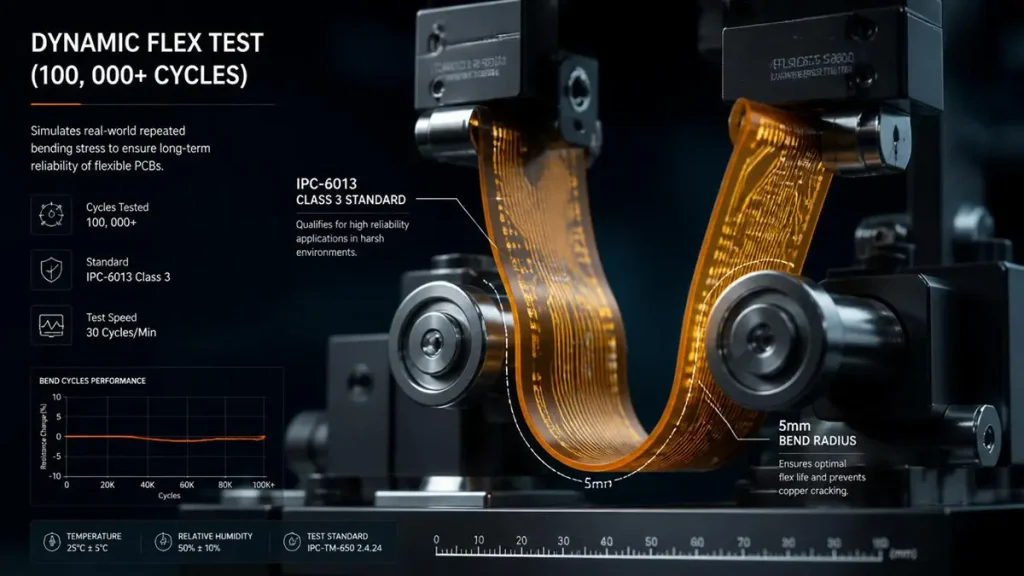
IPC-6013 Class 3 dynamic flex endurance testing setup demonstrating 100,000+ bending cycles at a 5mm bend radius.
Not all “flexible” PCBs are created equal. IPC-6013 defines three classes:
- Class 1: One-time flex for installation only. Unacceptable for wearables.
- Class 2: Occasional flexing. Marginal for fitness bands.
- Class 3: Dynamic flexing with ≥10,000 cycles at a specified bend radius.
For wearable ultra thin PCB procurement, Class 3 is the minimum viable standard. Verify that the supplier conducts dynamic bend testing per IPC-6013, measuring resistance change across 100,000 cycles at the design bend radius. Resistance variation exceeding 10% indicates cracked traces or via barrel failure.
At Hongda Circuit, our wearable flexible PCB qualification protocol includes:
- Dynamic flex test: 100,000 cycles at R5 mm bend radius, ΔR ≤ 10%
- Thermal cycling: −40°C to +85°C, 500 cycles, no delamination
- Damp heat: 85°C / 85% RH, 1,000 hours, insulation resistance > 100 MΩ
- Thermal stress: 3× 288°C reflow simulation, no layer separation
Material Science and Manufacturing Process: What Separates Production-Ready Wearable Flexible PCB Suppliers from Trading Companies
Adhesiveless Polyimide (TPI) vs. Standard Adhesive-Based Construction in Ultra Thin PCB for Wearable
The hidden failure mode in cheap wearable PCBs is the adhesive layer between copper and polyimide. Standard acrylic or epoxy adhesives add 12–20 µm of thickness but become brittle after thermal aging. In a health monitor worn 24/7, body heat and sweat accelerate adhesive degradation, leading to copper peel and open circuits.
Adhesiveless construction uses thermoplastic polyimide (TPI) as both substrate and bonding layer. This eliminates the weak interface, improves layer-to-layer adhesion, and reduces total thickness by 15–20%. For procurement teams, specifying “adhesiveless PI, no epoxy bond ply” in the RFQ filters out suppliers who rely on commodity flex materials.
Coverlay Selection and ENIG Surface Finish Requirements for Long-Term Wearable Reliability
Surface finish choice directly impacts solder joint life and contact resistance in wearable environments. For thin PCB for smartwatch assemblies with fine-pitch components (0.3–0.4 mm pitch BGA or CSP), we specify:
- ENIG (Electroless Nickel Immersion Gold): Ni ≥ 3 µm, Au ≥ 0.05 µm. Provides flat, coplanar pads essential for BGA placement and prevents nickel corrosion in humid conditions.
- Coverlay opening: Laser-cut coverlay apertures with ±25 µm registration accuracy, ensuring solder mask does not encroach on SMT pads.
Common procurement pitfall: Suppliers offering OSP or HASL on ultra-thin flex to reduce cost. OSP oxidizes during multiple reflow cycles; HASL creates uneven surfaces that prevent 0.3 mm pitch component placement. Both cause field failures in wearables.
Anti-Warpage Processing: Why 0.1 mm Mass Production Requires Vacuum Lamination and Precision Handling
Ultra-thin substrates warp during lamination, etching, and reflow. A 0.1 mm panel that bows 2 mm across a 200 mm span cannot be assembled by automated pick-and-place machines. Solving this requires process-level investment, not just careful handling.
At Hongda Circuit, our Lauffer vacuum lamination system applies uniform low-pressure across the panel surface, eliminating air gaps between layers and maintaining thickness tolerance within ±5 µm. Combined with carrier-panel processing during etching and automated conveyor systems that avoid mechanical stress, we achieve flatness suitable for high-speed SMT without manual flattening.
What to ask your supplier:“What is your standard bow and twist specification for 0.1 mm flex panels, and what lamination equipment do you use to achieve it?” If they mention standard hydraulic presses without vacuum capability, expect warpage-related assembly defects.
Shenzhen Hongda Circuit Technology’s 2026 Manufacturing Upgrade: Advanced Equipment for Wearable Ultra Thin PCB Production
Shenzhen Hongda Circuit Technology Co., Ltd. has completed a 2026 process upgrade specifically targeting wearable and foldable electronics. Our facility in Shenzhen operates a dedicated wearable flexible PCB production line with equipment configurations that match IC-substrate-level precision.
SCREEN Ledia LDI + mSAP Process: Achieving 20 µm/20 µm Line/Space on Ultra-Thin Substrates
Traditional subtractive etching on 18 µm copper foil cannot reliably produce lines below 50 µm due to isotropic undercut. For wearable ultra thin PCB designs requiring fine-pitch routing under BGA components, we deploy Modified Semi-Additive Process (mSAP) paired with SCREEN Ledia Laser Direct Imaging (LDI).
The mSAP workflow at Hongda Circuit:
- Laminate 1.5–3 µm ultra-thin copper seed layer on TPI substrate
- Image circuit pattern with LDI at ±1.5 µm registration accuracy
- Selectively plate copper to target trace height (15–20 µm)
- Flash-etch the seed layer, leaving near-vertical trace sidewalls
This achieves 20 µm/20 µm line/space in volume production and 8 µm/8 µm qualified for substrate-like PCB (SLP) builds. For wearable procurement teams, this means Bluetooth antenna traces and sensor interconnects that fit in 30% less area than subtractive-etched alternatives, enabling smaller product form factors without sacrificing signal integrity.
Mitsubishi UV/CO₂ Laser Drilling for 75 µm Microvias in Wearable Flexible PCB
Our Mitsubishi Electric UV/CO₂ hybrid laser drilling system processes microvias down to 50 µm diameter in 25 µm build-up dielectrics. The UV laser ablates copper cleanly; the CO₂ laser drills through polyimide without carbonization. This dual-source approach produces smooth via walls with no glass fiber protrusion—a common defect in mechanical drilling that causes plating voids and intermittent opens.
For thin PCB for smartwatch applications, this enables via-in-pad designs under 0.3 mm pitch components, reducing layer count and overall thickness.
Lauffer Vacuum Lamination and HX Automated Plating for 0.1 mm Rigid-Flex Volume Production
The transition from prototype to mass production is where most wearable PCB suppliers fail. Our Lauffer vacuum lamination system and HX Automation 3-in-1 horizontal plating line maintain process consistency across 1,000+ panel production runs. The plating line delivers uniform copper deposition in high-aspect-ratio microvias while reducing chemical consumption by 40% compared to conventional vertical lines.
Capacity note: We support 0.1 mm rigid-flex volume production with prototype turnaround of 3–5 days and mass production delivery of 2–3 weeks, with no minimum order quantity (MOQ) pressure for wearable startups validating designs.
AI-Driven Impedance Matching and Full-Process Quality Traceability
In 2026, we integrated an AI-driven impedance optimization algorithm into our design review workflow. For wearable flexible PCB projects, this simulates signal transmission paths during the stack-up design phase, predicting crosstalk and parasitic capacitance before fabrication. The result: Bluetooth antenna differential pairs controlled to 90Ω ±7% and high-speed digital lines at 50Ω ±10%, verified by TDR scanning on every production panel.
Full-process traceability means every panel has a serial number linked to lamination batch, plating chemistry lot, and AOI inspection images. If a field issue arises, we can trace it to the exact process step within 24 hours.
DFM Guidelines for Wearable PCB Procurement: Reducing Risk from Prototype to Mass Production
Panelization and Fiducial Design for High-Yield SMT Assembly of Thin PCB for Smartwatch
Ultra-thin boards are difficult to handle in automated assembly. We recommend:
- Tab routing with 0.3–0.5 mm process edge and 1.0 mm spacing between boards. This prevents flex damage during depanelization while maximizing material utilization.
- Global fiducials: Minimum 3 per panel, 1.0 mm diameter, clear of coverlay.
- Local fiducials: 2 per fine-pitch component site, ensuring SMT placement accuracy of ±25 µm.
Impedance Control for Bluetooth Antenna (90Ω ±7%) and High-Speed Signals in Wearable Devices
Wearable devices operate in a noisy RF environment. Uncontrolled impedance causes signal reflections that reduce Bluetooth range and corrupt sensor data. Our DFM review validates:
- 90Ω ±7% differential impedance for Bluetooth/NFC antenna traces
- 50Ω ±10% single-ended impedance for high-speed digital lines
- Continuous reference planes beneath critical traces—no splits or voids under routing channels
Stack-Up Design Review: How Hongda’s Engineering Team Prevents Costly Respins
Before fabrication begins, our engineers conduct a stack-up feasibility review that checks:
- Bend radius vs. layer count compatibility (more than 4 layers in a 3 mm bend radius invites failure)
- Copper weight distribution (asymmetric copper causes curl)
- Coverlay overlap onto pads (prevents soldering defects)
This review is provided at no charge and typically identifies 2–3 design issues that would otherwise require respins, saving 2–3 weeks in development time.
Application-Specific Solutions: Matching Wearable Flexible PCB Types to End-Use Requirements
hin PCB for Smartwatch Motherboards: Integrating RF Antennas, Charging Modules, and HDI Routing
A smartwatch motherboard is typically a 0.8 mm rigid-flex assembly: rigid sections for the MCU, PMIC, and eSIM; flex tails for the display connector and haptic engine. We integrate:
- Bluetooth antenna: 90Ω differential pair on outer flex layer with ground reference
- Wireless charging coil: Thick copper (2 oz) on dedicated flex layer to minimize I²R loss
- HDI routing: 3+N+3 any-layer interconnect to escape 0.35 mm pitch BGA
0.1 mm Flexible PCB for Health Sensor Modules: Heart Rate, Blood Oxygen, and Temperature Monitoring
Health sensor flex circuits require biocompatibility-grade materials and extreme thinness to maintain skin contact. Our 0.1 mm, 2-layer flex solutions for PPG (photoplethysmography) sensors use:
- Adhesiveless PI with matte copper for LED and photodiode mounting
- Open-window coverlay exposing sensor pads for direct skin or optical coupling
- Dynamic flex qualification: 10,000+ cycles at R3 mm to survive daily donning/doffing
AR/VR Headset Interconnects: Ultra-Thin Flexible Circuits for Display-to-Mainboard Connections
AR/VR headsets route high-speed video (MIPI DSI) from the mainboard to micro-OLED displays across hinge mechanisms. These wearable flexible PCB interconnects must:
- Carry 4-lane MIPI at 1.5 Gbps/lane without skew
- Survive 50,000+ fold cycles at the temple hinge
- Maintain thickness ≤ 0.2 mm to avoid bulk
We achieve this with shielded flex constructions: dual stripline routing between ground planes, with silver ink or copper mesh EMI shielding on the outer surfaces.
Why Procurement Teams Choose Shenzhen Hongda Circuit Technology Co., Ltd. for Wearable Ultra Thin PCB
Verified 2026 Capability: 0.1 mm Rigid-Flex and Flexible PCB Mass Production with Full Certifications
- ISO 9001 quality management
- IPC-A-600 and IPC-6013 Class 3 acceptance criteria
- RoHS and REACH material compliance
- UL recognition for flammability ratings
Our facility operates in a Class 1000 cleanroom environment for SLP and ultra-fine line processing, preventing particulate-induced shorts in 0.1 mm constructions.
Engineering-First Collaboration: From Gerber Review to DFM-Optimized Stack-Up Design
We do not quote from a price list. Every ultra thin PCB for wearable project begins with a 30-minute engineering call to review:
- Bend radius and flex cycle requirements
- Component placement and via strategy
- Impedance targets and material selection
This collaborative approach eliminates the “quote first, respin later” cycle that burns budget and schedule.Agile Delivery Model: 3–5 Day Prototypes, 2–3 Week Mass Production, No MOQ Pressure
Wearable hardware moves fast. Our production system supports:
- Prototype: 3–5 days for 0.1–0.2 mm flex and rigid-flex
- Pilot run: 1 week for 50–500 units
- Mass production: 2–3 weeks for 5,000+ units, with capacity scaling to 20,000 m²/month
No MOQ means health-tech startups can validate clinical prototypes without committing to 1,000-unit minimums.
Frequently Asked Questions by Wearable PCB Buyers
How Do I Verify That a Supplier Can Actually Manufacture 0.1 mm Ultra Thin PCB for Wearable Devices, Not Just Quote Them?
Request three verification documents: (1) a cross-sectional micrograph of their actual 0.1 mm production sample showing copper thickness and layer registration; (2) IPC-6013 Class 3 dynamic flex test data with resistance plots across 10,000+ cycles; (3) photographs of their lamination equipment—if they use standard hydraulic presses without vacuum capability for ultra-thin boards, they cannot control warpage. At Hongda Circuit, we provide all three during the qualification phase, plus a live video factory tour showing our Lauffer vacuum lamination and SCREEN LDI lines in operation.
What Is the Difference Between a Wearable Flexible PCB and a Standard Flex PCB, and Why Does It Matter for Pricing?
A standard flex PCB is designed for static installation (Class 1) with adhesive-based materials and solder mask. A wearable flexible PCB must meet IPC-6013 Class 3 dynamic flexing, use adhesiveless TPI substrates, polyimide coverlay instead of solder mask, and ENIG finish for fine-pitch assembly. These material and process upgrades add 20–35% to unit cost but prevent field failures that cost 10× more in warranty claims and brand damage. When comparing quotes, verify that both suppliers are quoting to the same material specification—not just the same thickness.
Why Should I Specify mSAP Instead of Standard Subtractive Etching for Thin PCB for Smartwatch Applications?
Subtractive etching on 18 µm copper cannot reliably produce traces below 50 µm due to undercut. For smartwatch motherboards with 0.35 mm pitch BGA and dense antenna routing, you need 15–30 µm line/space that only mSAP (Modified Semi-Additive Process) can achieve with vertical sidewalls and ±5% impedance tolerance. Suppliers without LDI + mSAP equipment will either refuse the design or outsource it, adding margin and risk. Hongda Circuit operates an in-house mSAP line with SCREEN Ledia LDI, achieving 20 µm/20 µm in volume and 8 µm/8 µm for advanced SLP builds
What DFM Mistakes Cause the Most Delays in Wearable Ultra Thin PCB Projects?
The top three DFM errors we correct during pre-fabrication review are: (1) asymmetric copper distribution—placing 2 oz copper on one side and 0.5 oz on the other causes the panel to curl after etching; (2) insufficient bend radius—designing a 6-layer flex to bend at R2 mm guarantees trace fracture within 1,000 cycles; (3) split reference planes under high-speed traces—voids in the ground plane beneath Bluetooth antenna pairs destroy impedance control and reduce range by 30–50%. Our engineering team catches these issues during stack-up review, before tooling charges are incurred.
How Do I Manage Supply Chain Risk When Sourcing Wearable Flexible PCB from China for Medical or Consumer Products?
Mitigate risk through four qualification layers: (1) Certification audit—verify ISO 9001, IPC membership, and material RoHS/REACH compliance; (2) Process audit—conduct a virtual or on-site factory tour focusing on whether the supplier owns their mSAP, LDI, and laser drilling equipment or outsources critical processes; (3) First-article inspection—require full cross-section, impedance TDR plots, and thermal cycle data on the first production lot; (4) Traceability system—confirm that every panel has a serial number linked to raw material batches and process parameters. Hongda Circuit provides full documentation packages including material certificates of conformance, IPC test reports, and serialized production records for every order.
Ready to source production-ready ultra-thin PCBs for your next wearable project?
Contact Shenzhen Hongda Circuit Technology Co., Ltd. at PCB@pcbkr.com for a free DFM review and technical quotation.
About Author
David Chen https://www.linkedin.com/in/pcbcoming
David Chen boasts an extensive professional background in PCBA manufacturing, PCBA testing, and PCBA optimization, with specialized expertise in high-precision PCBA fault analysis and rigorous PCBA reliability testing. The author has worked with high-layer-count server PCB fabrication, ultra-low-loss backplane stackups, and thermo-mechanical reliability optimization for AI infrastructure projects involving 112G and 224G PAM4 architectures. Skilled in complex circuit design and cutting-edge advanced PCB manufacturing processes, he delivers solutions that elevate product durability and performance across industrial applications. His technical articles focusing on PCBA manufacturing workflows and testing methodologies are widely cited by industry peers, research institutions, and technical platforms, solidifying his reputation as a recognized technical authority in the global circuit board manufacturing sector.