PLC Rack Backplane PCB Manufacturing: Custom Design, Fabrication & Assembly
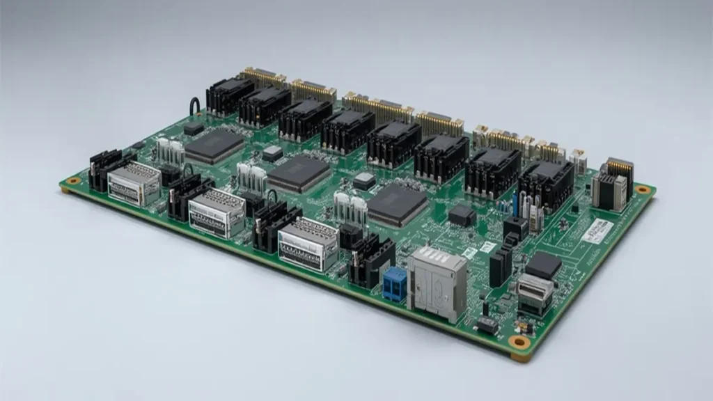
Base Material: FR-4 / High-Tg FR-4
Layer Count: 4–12 Layers
Board Thickness: 1.6–3.2 mm
Copper Thickness: 1–3 oz
Minimum Trace Width / Spacing: 4/4 mil
Minimum Hole Size: 0.20 mm
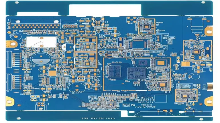
A PLC rack backplane PCB connects the processor, power supply, communication interface, and I/O modules installed in a modular PLC rack. Unlike a general PLC control board, its design must coordinate module slot positions, backplane bus connections, power distribution, and the mechanical interface between the PCB and plug-in modules. These requirements affect not only the circuit layout but also connector selection, board thickness, copper design, fabrication tolerances, assembly, and inspection.
For OEMs developing a new PLC platform or sourcing a custom industrial backplane, the manufacturing review should begin with the rack architecture and module interface—not simply the required PCB layer count. A supplier needs enough information to evaluate the electrical and mechanical requirements together before confirming manufacturability, cost, and lead time.
This guide explains the main design and manufacturing considerations for custom PLC rack backplane PCBs, from slot and connector layout to bus routing, power integrity, PCBA assembly, testing, and RFQ preparation.
1. PLC Rack Backplane Architecture and Main Functions
A PLC rack backplane is the shared electrical interconnection structure behind the modules installed in a modular controller. Depending on the platform, it may distribute power, carry communication signals, provide module identification or addressing connections, and establish the physical positions of the installed modules.
The exact architecture varies by PLC manufacturer and product family. Some backplanes are primarily passive interconnection boards; others include active electronic circuits for signal conditioning, bus management, protection, or monitoring. A backplane should therefore be evaluated against its actual system architecture rather than a generic PLC wiring diagram.
Power Distribution Between PLC Modules
The backplane commonly distributes one or more DC power rails from a power supply module to the CPU, I/O modules, and other rack components. The number of rails, voltage levels, current limits, and protection arrangements depend on the system.
For PCB manufacturing, the power design affects:
- Copper thickness and current-carrying capacity.
- Width and continuity of power distribution paths.
- Ground return paths and plane configuration.
- Connector pin allocation and contact-current requirements.
- Thermal rise around high-current traces, vias, and connector pads.
- Clearance and spacing around different voltage domains.
A backplane power design should be reviewed using the maximum expected load and the actual distribution topology. A nominal voltage value alone is not enough to determine copper requirements or connector suitability.
Backplane Bus Communication
The backplane bus provides communication paths between modules. Depending on the PLC platform, these may include parallel bus connections, serial communication, differential signaling, addressing lines, clock signals, or proprietary interfaces.
The PCB layout must preserve the electrical relationships defined by the system design. Relevant considerations include:
- Signal routing between module connectors.
- Ground reference continuity.
- Signal return paths and plane transitions.
- Crosstalk between adjacent signal groups.
- Termination and isolation components, where required.
- Connector pin mapping and routing consistency.
Not every PLC rack backplane uses high-speed differential signaling or requires controlled impedance. Those requirements should be determined from the interface specification, edge rate, signaling method, and system timing—not assumed from the word “backplane.”
Slot Configuration and Module Interconnection
The slot arrangement defines where each module connects to the backplane. It also determines connector placement, module spacing, board dimensions, and the relationship between the PCB and the rack chassis.
A manufacturing review should confirm:
- Total number of slots and their physical positions.
- Connector type and orientation at each slot.
- Pin assignment and electrical function by connector position.
- Board outline, mounting holes, and mechanical keep-outs.
- PCB thickness and connector engagement requirements.
- Any differences between CPU, power, communication, and I/O slots.
The slot map is a critical input for both PCB fabrication and assembly. A board can pass basic electrical continuity testing and still fail to fit the rack if the connector positions, board outline, or mechanical datum locations are incorrect.
2. Passive vs. Active PLC Rack Backplane PCB Design
The distinction between passive and active backplanes affects the manufacturing scope, component requirements, and test plan.
Passive PLC Backplane
A passive backplane primarily provides electrical connections between module connectors. It may contain copper routing, power planes, ground planes, and passive components, but it does not necessarily perform active bus processing.
Typical manufacturing considerations include:
- Multilayer routing for power and signal interconnections.
- Connector footprint and plated-hole accuracy.
- Copper distribution and isolation between power domains.
- Board thickness and flatness.
- Electrical continuity and insulation testing.
For a passive design, the main manufacturing risks are often associated with connector alignment, plated-through-hole quality, copper integrity, and the dimensional relationship between the PCB and rack.
Active PLC Backplane
An active backplane includes electronic components that perform functions such as signal buffering, bus management, termination, protection, monitoring, or other platform-specific operations.
In addition to bare-board requirements, active designs may require:
- Component placement and soldering controls.
- Fine-pitch SMT assembly.
- Through-hole connector soldering.
- AOI inspection and X-ray inspection where appropriate.
- Power-up checks and customer-defined functional testing.
- Component traceability and revision control.
The actual test scope depends on the circuit design and customer acceptance criteria. A supplier should not treat every active backplane as having the same functional test requirements.
Defining the Manufacturing Scope
Before requesting a quotation, clarify whether the supplier is expected to deliver:
| Manufacturing scope | Typical deliverable |
|---|---|
| PCB fabrication | Bare PLC rack backplane PCB |
| PCB fabrication + PCBA | Fabricated board with specified components and connectors assembled |
| Turnkey PCBA | PCB, approved component sourcing, assembly, and agreed inspection or testing |
| Build-to-print production | Manufacturing against customer-approved design and documentation |
This distinction prevents misunderstandings about connector sourcing, component procurement, assembly responsibility, and final testing.
3. PLC Rack Module Slots and Connector Layout
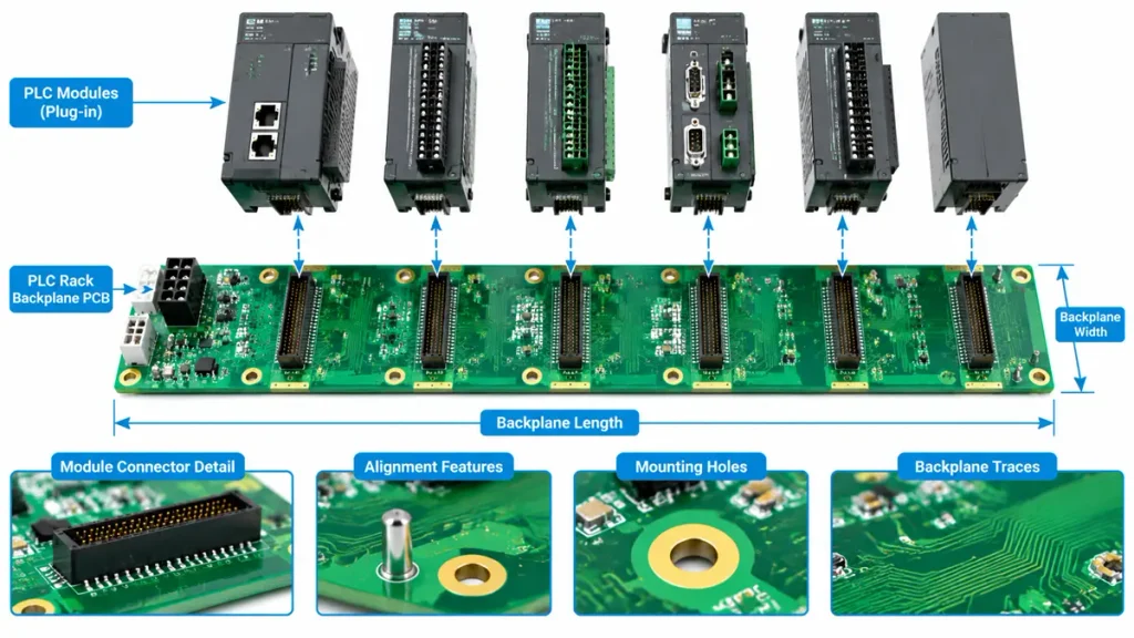
PLC Rack Backplane Module Slots and Connector Layout
The module interface is one of the most important parts of a PLC rack backplane. Connector positions must match the mechanical slot arrangement and the electrical pin assignment of the corresponding modules.
A supplier should review the connector drawing and rack mechanical documentation together with the PCB fabrication data. Reviewing only the Gerber files may not reveal all the mechanical constraints.
Slot Pitch and Connector Positioning
The slot pitch determines the spacing between adjacent modules. Connector placement must maintain the required alignment across the entire rack.
Important design inputs include:
- Slot count and slot-to-slot spacing.
- Connector center positions and orientation.
- Board datum points and mounting-hole coordinates.
- Connector height and mating direction.
- Chassis clearance and module insertion path.
- Tolerance accumulation across multiple slots.
For a long backplane, small positioning deviations can accumulate along the board. The mechanical drawing should identify the datum scheme and the tolerances that control connector alignment.
Connector Type and PCB Footprint
PLC rack backplanes may use through-hole, press-fit, SMT, or other connector technologies depending on the platform.
The connector manufacturer’s drawing should define the footprint and relevant mechanical requirements. The PCB manufacturer should review:
- Finished-hole diameter and tolerance.
- Hole position and pitch.
- Pad dimensions and annular ring.
- Plating requirements.
- Connector body clearance.
- Surface finish compatibility.
- Assembly method and inspection access.
For press-fit connectors, the finished-hole specification and plating structure are particularly important. The hole must meet the connector manufacturer’s requirements; a nominal drill size alone does not establish press-fit suitability.
Pin Assignment and Electrical Separation
Connector pin assignments should be checked against the approved schematic, interface specification, and module documentation.
The review should identify:
- Power and ground pins.
- Communication and control signals.
- Reserved or unused pins.
- Isolation boundaries, where applicable.
- High-current contacts.
- Any redundant or duplicated connections.
Power and signal pins should not be grouped or routed based only on physical convenience. Their arrangement must follow the electrical design and applicable safety requirements.
4. PLC Backplane Bus Architecture and Signal Integrity
A PLC backplane bus is not simply a collection of traces connecting adjacent slots. Its routing must preserve the intended electrical behavior between modules.
The correct layout approach depends on the bus topology, signaling method, data rate, edge speed, loading, connector characteristics, and the number of modules connected to the bus.
Bus Topology and Routing Structure
The design may use shared bus connections, point-to-point links, dedicated slot connections, or a combination of these structures.
The PCB layout should follow the approved topology. Changing a bus connection from a shared path to a branched path—or changing the routing length between slots—may affect signal behavior and system timing.
Before manufacturing, review:
- Bus topology and module connection sequence.
- Signal routing between connector pins.
- Branch lengths and stubs, if relevant to the interface.
- Reference-plane continuity.
- Ground and power plane transitions.
- Termination locations and component values.
- Connector pin mapping and routing symmetry, where required.
Signal Integrity and Ground Reference
For faster bus interfaces, routing geometry and reference-plane continuity may become important to signal quality. Potential issues include reflections, crosstalk, excessive skew, and discontinuities at connectors or vias.
Controlled impedance should be specified only when the electrical interface requires it. If the design includes defined impedance targets, the RFQ should provide the target values, tolerance, relevant signal layers, and stack-up requirements.
Where controlled impedance is required, the PCB supplier should review the proposed stack-up and trace geometry before fabrication. Test coupons and impedance measurement may be included when required by the approved specification.
For more demanding signal interfaces, see PCBKR’s High-Speed PCB manufacturing information. The need for high-speed design controls should still be confirmed against the actual PLC bus specification.
EMC and Noise Control
Industrial control cabinets may contain switching power supplies, motor drives, contactors, and other sources of electrical noise. The backplane’s grounding and routing strategy should therefore be considered as part of the complete control-system design.
PCB-level review may include:
- Separation of noisy power paths from sensitive signal paths.
- Continuous reference planes where the design permits.
- Appropriate return paths for switching and communication signals.
- Filtering and protection footprints specified by the circuit design.
- Ground connection strategy between modules.
- Connector pin allocation for ground and shielding interfaces.
PCB layout alone cannot guarantee system-level EMC compliance. The final result depends on the complete rack, enclosure, cabling, grounding, power supply, and installation environment.
5. PLC Rack Backplane Power Distribution Requirements
Power distribution is a major design consideration because the backplane may supply several modules through a shared connector and copper network.
The power architecture should be documented before PCB stack-up and copper requirements are finalized.
Power Rails and Current Requirements
The design package should identify each power rail, its nominal voltage, maximum current, expected load, and protection method.
A Texas Instruments application note describes a PLC power backplane as a shared structure for distributing power and data, and discusses protection concerns including current limiting, overvoltage, reverse-current blocking, inrush current, and surge protection. It also notes that typical backplane voltage levels vary by PLC system, so a single voltage range should not be treated as a universal design rule. ti.com
For each rail, the engineering review should establish:
- Maximum continuous current.
- Peak or transient current, if specified.
- Permitted voltage drop.
- Copper thickness and trace or plane geometry.
- Number of parallel connector contacts.
- Via count and current path.
- Thermal conditions and operating environment.
Copper Thickness and Current-Carrying Capacity
Copper weight is one factor in determining the current-carrying capacity of a backplane. The final design also depends on copper width, copper distribution, layer arrangement, thermal environment, allowable temperature rise, and the length of the current path.
A heavier copper specification does not automatically solve every power-distribution problem. It may affect etching, spacing, via design, and manufacturing cost. The appropriate construction should be evaluated against the actual current and temperature requirements.
For designs with demanding current loads, PCBKR’s Heavy Copper PCB manufacturing page may be relevant when evaluating copper construction options.
Voltage Drop and Thermal Management
Voltage drop across long copper paths or connector interfaces can cause modules to receive a voltage outside their specified operating range.
The design review should consider the complete path from the power input to each module slot, including:
- Copper resistance along the distribution path.
- Connector contact resistance.
- Via resistance and current sharing.
- Load variation between slots.
- Temperature rise under expected operating conditions.
If the backplane uses separate power groups or multiple feeds, their electrical boundaries and protection arrangements should be clearly identified in the design documentation.
Protection and Power Sequencing
Protection functions such as overcurrent limiting, reverse-current blocking, overvoltage protection, and inrush-current control may be implemented on the power supply, backplane, or individual modules.
The responsible circuit location must be defined by the system architecture. The PCB supplier should manufacture and assemble the specified design, not assume that every protection function belongs on the backplane.
For additional power-board design context, see PCBKR’s PCB for Power Supply page.
6. PCB Materials, Layer Stack-up and Manufacturing Specifications
PLC rack backplane PCB specifications should be selected according to electrical loading, mechanical dimensions, operating temperature, connector requirements, and the complexity of the routing.
There is no single standard layer count or material construction for every PLC backplane.
FR-4 and High-Tg Material Selection
FR-4 is commonly used for industrial control PCBs, but the appropriate grade should be selected based on the operating environment and manufacturing requirements.
Material review may include:
- Glass transition temperature (Tg).
- Thermal decomposition characteristics.
- Dielectric properties.
- Moisture absorption.
- Dimensional stability.
- Compatibility with the intended multilayer lamination process.
High-Tg material may be appropriate where the thermal environment or assembly process requires it. The selection should be based on the actual temperature profile and reliability requirements rather than choosing a material solely because it has a higher Tg value.
Multilayer Stack-up Design
A multilayer backplane may use dedicated power and ground planes to support current distribution and signal return paths. The layer count depends on the number of signals, connector pin density, routing topology, and electrical performance requirements.
The stack-up review should define:
- Total layer count.
- Core and prepreg construction.
- Finished board thickness.
- Copper weight by layer.
- Dielectric thickness.
- Signal, power, and ground layer allocation.
- Impedance requirements, if applicable.
- Finished-board flatness and dimensional tolerances.
The stack-up should be approved before production. Unapproved changes to dielectric thickness, copper weight, or material construction may affect impedance, board thickness, and connector fit.
Surface Finish and Connector Requirements
Surface finish should be selected according to the exposed copper features and component interface requirements.
The supplier should confirm whether the design requires ENIG, lead-free HASL, OSP, or another specified finish. Connector technology, solderability, contact design, and the applicable component requirements should guide the selection.
For press-fit connectors, the finished-hole and plating specifications must be reviewed against the connector manufacturer’s requirements. For soldered connectors, pad geometry, soldering process, and inspection criteria should be defined.
Mechanical Dimensions and Board Flatness
A backplane is both an electrical board and a mechanical interface. Board thickness, outline dimensions, mounting-hole locations, and flatness can affect module engagement.
The manufacturing drawing should specify the critical dimensions and tolerances. Where the board spans multiple slots, the datum system and connector-position tolerances should be reviewed before tooling and panelization are finalized.
7. PLC Backplane Connector Assembly and Mechanical Reliability
Connector assembly is a key manufacturing stage because the connectors establish the physical and electrical interface between the backplane and the installed modules.
The appropriate process depends on connector construction and the approved assembly documentation.
Through-Hole and SMT Connector Assembly
Through-hole connectors are commonly used where mechanical retention and electrical connection are required through the PCB. SMT connectors may be used where the connector design and mechanical loading permit surface mounting.
Assembly review should consider:
- Connector part number and approved revision.
- Pin pitch and footprint accuracy.
- Insertion direction and orientation.
- Solder joint accessibility.
- Thermal requirements during soldering.
- Mechanical support and retention.
- Inspection criteria for solder joints.
If the connector is press-fit, the insertion process and tooling requirements should be defined separately from conventional soldering.
Solder Joint and Connector Inspection
Connector defects can affect both electrical continuity and module engagement. Inspection should be selected according to the connector type and joint geometry.
Possible inspection methods include:
- Visual inspection of connector orientation and seating.
- AOI for accessible solder joints and components.
- X-ray inspection where hidden solder joints or specific connector structures justify it.
- Electrical continuity checks.
- Dimensional inspection of critical connector positions.
Not every connector assembly can be fully assessed by AOI or X-ray alone. The inspection plan should match the physical construction and the customer’s acceptance criteria.
Mechanical Reliability Considerations
The backplane’s mechanical environment may include repeated module insertion, vibration, thermal cycling, and cabinet-level mechanical stress.
The design and manufacturing review should consider:
- Connector retention and support.
- PCB thickness and local stiffness.
- Board mounting and screw locations.
- Connector alignment across the rack.
- Solder joint stress.
- Warpage limits.
- Environmental requirements specified by the OEM.
If insertion-cycle, vibration, or thermal-cycle testing is required, the test method and acceptance criteria should be provided by the customer or agreed during engineering review.
8. PLC Rack Backplane PCB Fabrication and PCBA Assembly Process
A controlled manufacturing process begins with a complete and approved data package. For a custom PLC rack backplane, the supplier should review both the electrical fabrication data and the mechanical interface information.
CAM and DFM Engineering Review
Before fabrication, the manufacturing team should review:
- Gerber or ODB++ files.
- NC drill data.
- Board outline and mechanical drawing.
- Stack-up and material specifications.
- Copper thickness and finished board thickness.
- Connector footprints and finished-hole requirements.
- Surface finish and tolerance requirements.
- Impedance requirements, where applicable.
The DFM review should identify manufacturability risks before production. These may include insufficient annular ring, unsuitable finished-hole dimensions, connector pad issues, copper-spacing conflicts, or stack-up inconsistencies.
Any proposed change affecting electrical or mechanical performance should be submitted for customer approval before implementation.
Multilayer PCB Fabrication
The fabrication process may include inner-layer imaging, etching, lamination, drilling, plating, outer-layer imaging, solder mask application, surface finishing, routing, and electrical testing.
For a PLC backplane, particular attention should be paid to:
- Layer-to-layer registration.
- Plated-through-hole quality.
- Finished-hole dimensions.
- Copper integrity in power paths.
- Board thickness and flatness.
- Connector footprint accuracy.
- Final board outline and mounting-hole position.
The applicable process controls and acceptance criteria should be defined by the drawing, purchase specification, and agreed quality requirements.
PCBA Assembly
For active backplanes or designs requiring connector installation, assembly may include SMT placement, through-hole soldering, connector insertion, and other customer-specified processes.
The assembly package should contain a controlled BOM, placement data, assembly drawings, component orientation information, and any special process instructions.
The supplier should also confirm whether components are customer-supplied or supplier-sourced and whether substitutions require written approval.
Prototype and Production Scaling
Prototype builds are useful for confirming mechanical fit, connector engagement, electrical continuity, and assembly feasibility before volume production.
For a new design, the first-article review may include:
- Board outline and thickness verification.
- Slot and connector position measurement.
- Connector seating and orientation checks.
- Bare-board electrical test results.
- Assembly inspection records.
- Customer-defined power-up or functional test results.
After prototype approval, the released data package should be controlled by revision to prevent differences between sample and production builds.
9. Electrical Testing and Quality Control for PLC Backplane PCBs
Testing should distinguish between bare-board verification, assembly inspection, and system-level functional validation. These are different activities and should not be treated as interchangeable.
Bare PCB Electrical Testing
Bare-board electrical testing checks the fabricated PCB against the approved netlist or test data.
Depending on the specification, this may include:
- Open-circuit detection.
- Short-circuit detection.
- Continuity verification.
- Insulation resistance testing, where specified.
- Verification of defined electrical nets.
A successful bare-board electrical test does not prove that the complete PLC rack will communicate correctly or distribute power properly under operating load.
Connector and Assembly Inspection
For assembled backplanes, inspection may include:
- Connector presence and part-number verification.
- Polarity and orientation checks.
- Solder joint inspection.
- AOI for applicable components and joints.
- X-ray for suitable hidden-joint structures.
- Assembly workmanship inspection.
The inspection method should be selected based on the actual assembly structure.
Power Distribution Verification
Where required by the customer, power-related tests may verify continuity between the power input and designated slot contacts, polarity, isolation between rails, and voltage behavior under specified test conditions.
Load testing or temperature-rise evaluation should only be claimed when the test setup, load conditions, measurement method, and acceptance limits are defined and performed.
Functional Testing Based on Customer Requirements
A complete PLC rack functional test may require the actual CPU, power supply, I/O modules, communication modules, firmware, and test fixtures. A PCB manufacturer may not have access to the customer’s complete system configuration.
The RFQ should therefore identify which party is responsible for system-level validation and what evidence the PCB or PCBA supplier must provide.
10. PLC Rack Backplane PCB Manufacturing Cost Factors
The cost of a custom PLC rack backplane depends on more than the board’s dimensions or layer count. Connector requirements, mechanical tolerances, material construction, assembly scope, and testing can all affect the quotation.
| Cost factor | Potential cost impact |
|---|---|
| Board dimensions | Material usage, panel utilization, routing and handling |
| Layer count | Lamination complexity, drilling and registration controls |
| Copper thickness | Material and etching process requirements |
| PCB material | Material grade, availability and thermal requirements |
| Connector type | Component cost, hole tolerances, insertion or soldering process |
| Surface finish | Finish selection and processing requirements |
| Mechanical tolerances | Additional process control and inspection |
| PCBA scope | Component sourcing, SMT, through-hole assembly and inspection |
| Testing | Electrical fixtures, functional test setup and documentation |
| Order quantity | Setup cost allocation, panel utilization and production planning |
For a more accurate quotation, the buyer should specify whether the request covers bare PCB fabrication, connector assembly, complete PCBA, or turnkey supply. Comparing quotations with different manufacturing scopes can lead to misleading price decisions.
11. What to Prepare Before Requesting a PLC Backplane PCB Quote
A complete RFQ package allows the supplier to evaluate the backplane’s manufacturing requirements without making assumptions about the rack interface.
The following information is particularly useful.
PCB Fabrication Files
- Gerber or ODB++ fabrication files.
- NC drill files.
- Board outline and mechanical drawing.
- Layer stack-up.
- Copper weight by layer.
- Finished board thickness.
- Surface finish.
- Critical dimensional tolerances.
- Electrical test requirements.
Rack and Connector Documentation
- Rack mechanical drawing.
- Slot map and slot pitch.
- Connector manufacturer and part numbers.
- Connector datasheets and footprint drawings.
- Pin assignment and interface mapping.
- Finished-hole and plating requirements.
- Mounting-hole and datum information.
- Board-to-chassis clearance requirements.
Electrical and Functional Requirements
- Power rail definitions and maximum current.
- Signal and bus interface specifications.
- Impedance requirements, if applicable.
- Grounding and isolation requirements.
- Protection circuit requirements.
- Operating temperature range.
- Required electrical and functional tests.
- Customer acceptance criteria.
Commercial and Production Information
- Prototype and production quantities.
- Required manufacturing scope: PCB, PCBA, or turnkey.
- Component sourcing responsibility.
- Target delivery schedule.
- Required inspection reports and traceability.
- Applicable quality standards and documentation requirements.
For replacement projects, provide the exact platform, rack model, board revision, connector details, slot configuration, and available system documentation. A visually similar board should not be assumed to be electrically or mechanically interchangeable. Industrial control hardware documentation also emphasizes the importance of matching the backplane configuration and mechanical installation details during replacement. support.rockwellautomation.com+1
12. Custom PLC Rack Backplane PCB Manufacturing by PCBKR
PCBKR supports custom PCB fabrication and PCBA assembly for OEM projects. For PLC rack backplane enquiries, the manufacturing scope should be reviewed against the customer’s released design files, connector specifications, electrical requirements, and mechanical drawings.
A project review can be organized around the following items:
Custom PCB fabrication
- Gerber or ODB++ data review.
- Layer stack-up and material requirements.
- Board thickness and copper specifications.
- Finished-hole and connector footprint requirements.
- Surface finish and dimensional tolerances.
PCBA assembly
- BOM and component revision review.
- SMT and through-hole assembly requirements.
- Connector type, orientation, and assembly method.
- Inspection and test requirements.
Engineering and production review
- Slot layout and connector alignment.
- Power distribution and copper requirements.
- Bus routing and impedance requirements, where specified.
- Prototype and production quantity planning.
- Open technical issues requiring customer confirmation.
PCBKR’s manufacturing proposal should be based on the actual project scope and approved technical documentation. Specific layer counts, material grades, connector processes, tolerances, testing coverage, and delivery schedules should be confirmed during quotation rather than assumed from a generic capability statement.
For a custom PLC rack backplane PCB quotation, send the fabrication files, BOM if assembly is required, rack and connector drawings, and the required quantity to sales@pcbkr.com. This gives the engineering and sales teams a basis for reviewing the manufacturing scope and identifying missing technical information.
13. Frequently Asked Questions About PLC Rack Backplane PCB Suppliers
How Do I Find a Manufacturer for a Custom PLC Rack Backplane PCB?
Look for a PCB manufacturer that can review multilayer fabrication requirements, connector footprints, finished-hole tolerances, board thickness, and mechanical alignment. If the project requires an assembled backplane, confirm that the supplier can also handle the specified SMT or through-hole connector assembly.
When comparing suppliers, provide the same Gerber or ODB++ files, stack-up, connector drawings, BOM, and inspection requirements to each manufacturer. This makes quotations easier to compare on an equivalent technical scope.
Can a PCB Manufacturer Produce a Custom PLC Rack Backplane Based on My Gerber Files?
Yes. A manufacturer can evaluate a custom backplane using customer-provided Gerber or ODB++ files, provided the package contains sufficient fabrication information.
For an accurate review, also provide the stack-up, drill data, board outline, connector drawings, finished-hole specifications, and critical mechanical tolerances. If the board is part of an existing PLC platform, include the relevant rack and module interface documentation.
Can You Manufacture Both the PLC Backplane PCB and the Assembled PCBA?
This depends on the supplier’s manufacturing scope. A project may require bare PCB fabrication only, PCB fabrication with connector installation, or a complete PCBA with active components and connectors.
For an assembled backplane, the RFQ should include the BOM, component part numbers, placement data, assembly drawings, connector specifications, and inspection requirements. Confirm whether component sourcing, substitutions, and functional testing are included in the quotation.
What Information Do I Need to Request a PLC Rack Backplane PCB Quote?
At minimum, prepare the Gerber or ODB++ files, NC drill data, board outline, stack-up, board thickness, copper specifications, surface finish, and required quantity.
For a rack backplane, also provide the slot layout, connector part numbers, pin assignment, mechanical drawings, power requirements, and bus interface specifications. If PCBA is required, include the BOM and assembly documentation. Incomplete connector or mechanical information may prevent the supplier from confirming manufacturability and quotation assumptions.
Can a Custom PLC Rack Backplane PCB Replace an Existing Backplane?
A custom-manufactured board may be produced against an existing design or an approved replacement design, but physical similarity alone does not establish compatibility.
Before approving a replacement, verify the PLC platform, rack model, hardware revision, slot configuration, connector pinout, power distribution, bus architecture, board dimensions, and mounting details. The replacement should be validated against the original system documentation and the customer’s acceptance requirements.
About Author
David Chen LinkedIn Profile
David Chen is a Senior RF/PCB Process Engineer at Shenzhen Hongda Circuit Technology Co., Ltd., with over 12 years of experience in high-frequency PCB fabrication, impedance-controlled stack-up design, and Rogers/PTFE laminate processing. He also boasts an extensive professional background in PCBA manufacturing, PCBA testing, and PCBA optimization, with specialized expertise in high-precision PCBA fault analysis and rigorous PCBA reliability testing. The author has worked with high-layer-count server PCB fabrication, ultra-low-loss backplane stackups, and thermo-mechanical reliability optimization for AI infrastructure projects involving 112G and 224G PAM4 architectures. Skilled in complex circuit design and cutting-edge advanced PCB manufacturing processes, he delivers solutions that elevate product durability and performance across industrial applications. His technical articles focusing on PCBA manufacturing workflows and testing methodologies are widely cited by industry peers and technical platforms, and have gained attention and recognition from industry colleagues.
PLC Rack Backplane PCB – Data Sheet
| Item | Specification |
|---|---|
| Product Type | PLC Rack Backplane PCB |
| PCB Type | Custom Industrial Control Backplane |
| PCB Material | FR-4 / High-Tg FR-4 |
| Layer Count | Custom Multilayer |
| Board Thickness | Customizable |
| Copper Thickness | Customizable by Layer |
| Minimum Trace Width / Spacing | Based on Design Requirements |
| Minimum Hole Size | Based on Connector and Design Requirements |
| Surface Finish | ENIG / Lead-Free HASL / OSP |
| Solder Mask | Green / Black / Blue / Other Custom Colors |
| Silkscreen | White / Other Custom Colors |
| PCB Structure | Passive or Active Backplane |
| Connector Type | Through-Hole / SMT / Press-Fit |
| Slot Configuration | Custom Module Slot Layout |
| Bus Interface | Defined by Customer Design |
| Power Distribution | Custom Power Rail Configuration |
| Impedance Control | Available When Required by Design |
| PCB Fabrication | Multilayer PCB Manufacturing |
| Assembly Process | SMT / Through-Hole Assembly |
| Inspection | AOI / X-Ray / Electrical Testing, as Applicable |
| Electrical Testing | Open / Short Circuit Testing |
| Functional Testing | According to Customer Specifications |
| Production Volume | Prototype / Small Batch / Mass Production |
| Application | PLC Racks, Industrial Automation and Modular Control Systems |
Optional Engineering Requirements
- Custom connector positioning and pin assignment
- Controlled impedance for specified bus interfaces
- Heavy copper power distribution
- High-Tg material selection
- Connector soldering and inspection
- Power rail continuity and isolation verification
- Customer-defined functional testing
Note: The specifications above are configurable reference options, not fixed specifications for every PLC rack backplane. Final material, layer count, board thickness, copper weight, trace width/spacing, hole size, connector construction, impedance requirements, and inspection scope must be confirmed according to the customer’s Gerber files, BOM, mechanical drawings, electrical specifications, and acceptance criteria.