
What Should You Look for in a CPE PCBA Manufacturing Partner?
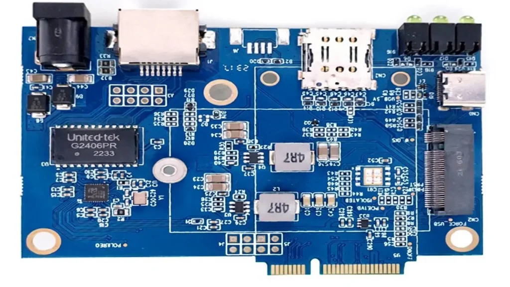
PCB Material: FR‑4; high‑frequency/hybrid laminates per design
Layer Count: Multilayer, customized by circuit complexity
Board Thickness: Customized for mechanical & stack‑up needs
Copper Thickness: Customized for current & signal demands
Min Trace Width / Spacing: Per layout & DFM review
Min Hole Size: Per via, component & DFM review
CPE PCBA manufacturing and assembly requires more than basic SMT placement. PCBKR supports custom PCB fabrication and PCBA assembly for Customer Premises Equipment projects, with engineering review of board files, component packages, assembly requirements, inspection and agreed testing scope. Send your Gerber files, BOM and project requirements to sales@pcbkr.com for a manufacturing assessment and quotation.
CPE PCBA Manufacturing for Customer Premises Equipment
Customer Premises Equipment (CPE) connects a user’s local network or devices to a service provider’s communication infrastructure. Depending on the product, CPE hardware may include broadband gateways, fiber terminals, wireless access equipment, 5G fixed wireless access devices and network interface units.
These products often combine digital processing, memory, power management, wired network interfaces and wireless communication circuits on one or more printed circuit boards. Their PCBA requirements therefore depend on the product architecture, component selection, electrical specifications and intended operating environment.
PCBKR provides PCB fabrication and PCBA assembly for custom electronic board projects. For CPE manufacturers and OEM engineering teams, the manufacturing scope can be reviewed according to the supplied design files and project requirements.
Typical project requirements may include:
- Multilayer PCB fabrication for communication and control boards.
- SMT and through-hole component assembly.
- Fine-pitch IC, BGA and QFN package assembly, subject to design and process review.
- Assembly of Ethernet connectors, power components and communication-related components.
- AOI, X-ray and applicable electrical inspection.
- Testing according to customer-defined procedures and acceptance criteria.
The exact manufacturing route is determined by the board design, BOM, component packages, production quantity and required inspection or testing scope.
CPE Mainboard PCB Fabrication Requirements
The PCB is the manufacturing foundation of a CPE mainboard. Layer count, material selection, copper thickness, finished board thickness, surface finish and stack-up all influence fabrication feasibility and assembly performance.
Before production, the engineering review should establish the requirements that affect the manufacturing process.
Layer Count and PCB Stack-Up
CPE mainboards may use multilayer structures to accommodate processors, memory, power circuits, Ethernet interfaces and wireless-related components. The actual layer count depends on routing density, electrical requirements and the mechanical dimensions of the product.
The fabrication package should identify:
- Total PCB layer count.
- Finished board thickness and tolerance.
- Copper weight for each layer.
- Core and prepreg requirements.
- Surface finish.
- Controlled-impedance requirements, where applicable.
- Board outline, slots and mechanical tolerances.
A complete stack-up drawing helps prevent assumptions about material thickness and impedance during quotation. If the customer requires a specific stack-up, it should be included in the manufacturing data rather than left to interpretation.
Material and Signal Routing Considerations
Material selection should follow the electrical and environmental requirements of the actual design. Standard FR-4 may be appropriate for many CPE control and interface boards. Designs with more demanding high-frequency or signal-integrity requirements may require a different laminate or a hybrid stack-up.
For boards requiring advanced interconnection density, PCBKR can review whether HDI structures and microvias are suitable for the supplied design. Related manufacturing information is available in our HDI PCB manufacturing page.
Material selection should not be based on product labels alone. The design’s operating frequency, dielectric requirements, loss budget, impedance targets and manufacturing tolerances should guide the decision.
Controlled Impedance and High-Frequency Requirements
Some CPE boards contain high-speed digital interfaces or RF-related signal paths. These designs may require controlled impedance, defined reference planes, suitable dielectric properties and consistent copper geometry.
For an engineering review, the customer should provide:
- Target impedance values and tolerances.
- Relevant signal-layer information.
- Reference-plane and stack-up requirements.
- Trace geometry or design data.
- Any specified impedance coupon or test requirements.
PCBKR’s high-frequency PCB manufacturing information can be reviewed on the High Frequency PCB page.
Controlled-impedance fabrication does not, by itself, verify the performance of a complete CPE device. System-level signal integrity, RF performance and network operation must be evaluated using the customer’s design and test procedures.
Processor, Memory and Fine-Pitch Component Assembly
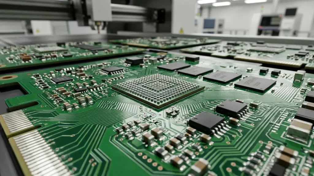
BGA and QFN component assembly for CPE mainboard manufacturing, supporting compact processor and memory integration.
CPE mainboards may integrate application processors, network processors, memory devices, storage components and power-management ICs. These components can use fine-pitch packages that require careful coordination between PCB design and assembly processes.
BGA and QFN Assembly Considerations
BGA and QFN packages require attention to land patterns, solder-mask design, stencil apertures, component coplanarity and the selected reflow process.
For BGA assembly, important review items include:
- Package dimensions and ball pitch.
- PCB pad geometry and solder-mask definition.
- Component moisture sensitivity and handling requirements.
- Reflow profile requirements.
- X-ray inspection criteria.
- Customer-defined acceptance standards.
X-ray inspection is particularly relevant to solder joints that cannot be visually inspected after assembly, including joints beneath BGA packages. Inspection criteria should be agreed before production.
QFN and other bottom-terminated packages also require suitable pad and stencil design. Voiding, solder coverage and thermal considerations should be evaluated against the component manufacturer’s guidance and the customer’s acceptance requirements.
SMT and Through-Hole Assembly
CPE boards may combine surface-mount devices with through-hole connectors, ports, switches or other mechanical interface components.
The assembly plan should identify:
- SMT component placement and orientation.
- Through-hole component locations.
- Connector alignment and mechanical requirements.
- Polarity-sensitive components.
- Components requiring special handling.
- Any selective soldering or manual assembly operations.
Clear assembly drawings and complete placement data reduce ambiguity during manufacturing.
RF and Wireless Circuit Assembly for CPE Boards
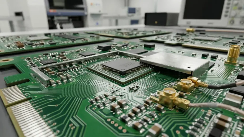
RF and wireless circuit assembly for CPE communication boards, including RF components, antenna connectors and signal-related circuitry.
Wireless CPE products may include RF transceivers, wireless modules, antenna connectors, matching components and related signal paths. The exact configuration depends on the product design and supported communication technology.
From a PCBA manufacturing perspective, the important issue is to ensure that the PCB and assembly requirements match the approved design.
RF Components and Connector Assembly
RF-related assembly may involve small passive components, shielding structures, coaxial connectors and wireless modules. Their placement and soldering quality can affect the electrical connection and mechanical reliability of the board.
The RF assembly review should consider:
- Component package and placement requirements.
- RF connector footprint and mechanical support.
- Ground connections and shielding requirements.
- Soldering specifications for RF connectors.
- Clearance and keep-out areas defined by the PCB design.
- Inspection and electrical test requirements.
PCB assembly quality is one part of RF product performance. Antenna tuning, radiated performance, wireless protocol validation and regulatory testing are separate activities that must be defined in the customer’s product validation plan.
RF Measurement and Test Scope
Where a project requires RF-related measurements, the customer should specify the measurement points, frequency range, test method, limits and required report format.
PCBKR has VNA measurement capability up to 70 GHz. The availability and suitability of a specific measurement for a CPE project must be confirmed against the board design, test setup and project requirements.
This distinction matters: a manufacturer’s measurement equipment capability should not be interpreted as automatic certification of a finished wireless device.
Ethernet, WAN/LAN and Power Management Assembly
Wired network interfaces and power circuits are important parts of many CPE mainboards. Their assembly requirements should be reviewed separately because they involve different component types and inspection considerations.
Ethernet and Network Interface Components
Depending on the design, Ethernet interfaces may include:
- RJ45 connectors.
- Ethernet PHY devices.
- Network transformers or magnetics.
- ESD protection components.
- Interface filters and supporting passive components.
Connector alignment and solder-joint quality are important for boards exposed to repeated cable insertion and removal. The assembly drawing should identify connector orientation, mechanical support and any special soldering requirements.
Where the customer requires electrical verification, the test procedure should define the applicable interface checks and pass/fail limits.
Power Management Circuit Assembly
Power-management circuits may include DC-DC converters, regulators, inductors, capacitors, protection devices and power connectors.
The BOM and assembly data should clearly identify component values, ratings, package types and reference designators. If a component has multiple possible variants, the correct build configuration must be confirmed before assembly.
Thermal performance, voltage regulation and power sequencing are primarily design and system-validation requirements. PCBA manufacturing should follow the approved design and the customer’s specified inspection and test procedures.
CPE PCBA Inspection and Testing
Inspection and testing should be selected according to the board design, component packages, product risk and customer acceptance requirements. No single inspection method can verify every aspect of a completed CPE board.
PCBKR uses inspection and test methods including 3D AOI, X-ray and four-wire Kelvin flying probe testing. Their use depends on the product design and the agreed manufacturing scope.
| Inspection or test method | Typical purpose | Important limitation |
|---|---|---|
| 3D AOI | Checks visible component placement, polarity and solder-joint conditions within inspection coverage | Cannot inspect hidden BGA solder joints |
| X-ray inspection | Examines hidden solder connections, including BGA joints | Requires defined inspection criteria and does not replace functional testing |
| Four-wire Kelvin flying probe | Performs applicable electrical measurements with reduced lead-resistance influence | Test coverage depends on accessible test points and the agreed test program |
| Functional testing | Verifies specified board functions under defined operating conditions | Requires customer test procedures, fixtures, firmware or other project inputs as applicable |
Defining the Testing Scope Before Production
A quotation should distinguish between visual inspection, electrical testing and functional testing.
For example, AOI can identify certain assembly defects, while X-ray can help inspect hidden solder connections. Flying probe testing can check specified electrical characteristics. Functional testing requires an agreed test method and defined pass/fail limits.
Before production, the customer and manufacturer should confirm:
- Which inspection methods are required.
- Whether testing applies to every board or a sample.
- Required test points and electrical limits.
- Whether firmware programming is included.
- Whether the customer supplies test fixtures and procedures.
- What inspection or test records are required for delivery.
A clearly defined test scope prevents misunderstandings about what a statement such as “tested PCBA” actually includes.
Component Sourcing and Turnkey CPE PCBA Assembly
Component procurement can affect both quotation accuracy and production scheduling. A CPE BOM may contain processors, memory devices, communication ICs, connectors and passive components with different availability and lifecycle conditions.
The purchasing arrangement should be established before the order is released.
Customer-Supplied Components
In a customer-supplied arrangement, the customer provides some or all of the electronic components. The RFQ should identify the supplied parts, quantities, delivery schedule, packaging requirements and any approved component sources.
The manufacturer should receive a complete and traceable component list to coordinate incoming materials with the production plan.
Manufacturer-Coordinated Component Procurement
Where component procurement is included in the agreed project scope, the BOM should identify manufacturer part numbers, approved alternatives and any restrictions on sourcing channels.
Before approving a quotation, buyers should clarify:
- Which components are included in the quotation.
- Whether alternative parts are permitted.
- Who approves proposed substitutions.
- How shortages and obsolete components are handled.
- Whether material traceability documents are required.
No component substitution should be made solely because a part appears electrically similar. Package, pinout, ratings, firmware compatibility and customer approval requirements must be considered.
Turnkey and Partial-Turnkey Project Scope
A turnkey quotation may combine PCB fabrication, component procurement, assembly and agreed inspection or testing. A partial-turnkey project may divide material responsibilities between the customer and manufacturer.
The quotation should state which party is responsible for each part of the supply chain. It should also identify excluded items such as enclosure assembly, cable harnesses, firmware development or system-level validation when these are outside the requested PCBA scope.
CPE PCBA Prototype, NPI and Production Requirements
A CPE project may move through prototype, engineering validation, pilot production and recurring manufacturing. Each stage has different priorities.
Prototype and Engineering Builds
Prototype builds help customers evaluate whether the supplied design and manufacturing process meet the project’s requirements.
Before assembly, the manufacturer should review the latest Gerber data, BOM, placement file and assembly drawings. Any discrepancies between document revisions should be resolved before production.
Pilot Production and Process Confirmation
Pilot production can help identify assembly or material issues that may not be apparent from a small prototype build. It also gives the customer an opportunity to confirm inspection criteria, packaging and production documentation.
The pilot build should use an approved design revision and clearly defined acceptance requirements.
Repeat Production and Revision Control
For repeat orders, revision control is essential. A change to the PCB layout, BOM, component source or assembly instruction may affect manufacturing and inspection.
Customers should provide a formal revision identifier and updated files for each approved change. The manufacturer should not assume that a new file automatically replaces an earlier approved version without confirmation.
CPE PCBA RFQ Requirements and Quotation Process
A complete RFQ allows the engineering and purchasing teams to evaluate the same manufacturing scope. It also helps reduce quotation delays caused by missing component information or unclear test requirements.
For a CPE PCBA quotation, prepare the following information where available.
| RFQ document or information | What it should contain |
|---|---|
| Gerber or ODB++ files | PCB copper, solder mask, silkscreen and board outline data |
| NC drill files | Hole locations and drill information |
| PCB fabrication drawing | Layer count, thickness, copper weight, finish and tolerances |
| Stack-up information | Material construction and controlled-impedance requirements, if applicable |
| BOM | Reference designators, quantities, manufacturer names and part numbers |
| Pick-and-place file | Component coordinates, rotation and placement information |
| Assembly drawing | Polarity, orientation, special instructions and component variants |
| Inspection and test requirements | AOI, X-ray, electrical test and functional test scope |
| Quantity and schedule | Prototype quantity, production quantity and target delivery date |
| Commercial requirements | Component sourcing arrangement, packaging, labeling and shipping destination |
If the complete document package is not yet available, buyers can initially provide the product type, board dimensions, estimated quantity and a brief project description. The missing information can then be identified before a firm quotation is prepared.
What Affects CPE PCBA Cost and Lead Time?
CPE PCBA pricing depends on more than the number of components on the board. Important factors include:
- PCB layer count, material and fabrication complexity.
- Board dimensions, copper weight and surface finish.
- BGA, QFN and other fine-pitch package requirements.
- Component availability and sourcing arrangement.
- SMT and through-hole assembly operations.
- Inspection coverage and testing requirements.
- Prototype quantity and recurring production volume.
- Special packaging, labeling and documentation requirements.
A quotation should separate PCB fabrication, components, assembly, inspection, testing and other requested services where applicable. This makes it easier for procurement teams to compare offers on an equivalent basis.
Request a CPE PCBA Manufacturing Quote from PCBKR
PCBKR works with customers on custom PCB fabrication and PCBA assembly projects. For CPE mainboards and communication-related electronic boards, the manufacturing scope is assessed according to the actual design files, component requirements, production quantity and inspection or test plan.
To start a quotation review, send:
- Your latest Gerber or ODB++ files.
- BOM with manufacturer part numbers.
- Pick-and-place data and assembly drawings.
- PCB specifications and stack-up requirements.
- Prototype and production quantities.
- Required inspection, electrical testing or functional testing scope.
If your design includes BGA, QFN, RF components, controlled-impedance routing or other special requirements, identify them in your inquiry so they can be reviewed during the quotation process.
Contact PCBKR for CPE PCBA manufacturing and assembly:
Email: sales@pcbkr.com
Website: https://www.pcbkr.com/
Send your CPE PCBA project files and requirements to discuss manufacturing feasibility, assembly scope and quotation details.
Frequently Asked Questions About CPE PCBA
What files are required for a CPE PCBA manufacturing quotation?
A typical CPE PCBA RFQ should include Gerber or ODB++ files, NC drill data, a PCB fabrication drawing, BOM, Pick-and-Place file and assembly drawings. Include stack-up information, target quantities, delivery requirements and inspection or testing specifications where applicable. These documents allow the manufacturer to review PCB fabrication, component assembly and quotation scope.
Can PCBKR manufacture and assemble CPE mainboard PCBs with BGA and QFN components?
PCBKR can review CPE mainboard projects involving fine-pitch components, including BGA and QFN packages, according to the supplied PCB design, component specifications and assembly requirements. X-ray inspection is available for applicable hidden solder-joint inspection. Package pitch, pad design, board construction and inspection criteria should be confirmed during engineering review.
Does CPE PCBA manufacturing include RF and wireless component assembly?
CPE boards may contain RF modules, wireless components, antenna connectors and related passive devices. PCBKR can assess the PCB fabrication and assembly requirements from the customer’s design files. RF performance validation, antenna tuning and complete wireless-device certification are separate activities and must be specified and arranged according to the project scope.
Can I order PCB fabrication and PCBA assembly together for a CPE project?
PCB fabrication and PCBA assembly can be reviewed together as one project scope. The quotation should identify the bare PCB specifications, BOM, component supply arrangement, assembly operations, inspection requirements and any agreed testing. Customers should confirm whether components are supplied by the customer or included in an agreed procurement scope.
What determines CPE PCBA manufacturing cost and lead time?
The main factors include PCB layer count, material, board dimensions, fabrication tolerances, component packages, BOM availability, assembly complexity, production quantity and testing requirements. Incomplete BOM information or unclear component alternatives can delay quotation and production planning. Providing the latest design files and a clear RFQ scope helps the manufacturer prepare a more accurate quotation.
About Author
David Chen LinkedIn Profile
David Chen is a Senior RF/PCB Process Engineer at Shenzhen Hongda Circuit Technology Co., Ltd., with over 12 years of experience in high-frequency PCB fabrication, impedance-controlled stack-up design, and Rogers/PTFE laminate processing. He also boasts an extensive professional background in PCBA manufacturing, PCBA testing, and PCBA optimization, with specialized expertise in high-precision PCBA fault analysis and rigorous PCBA reliability testing. The author has worked with high-layer-count server PCB fabrication, ultra-low-loss backplane stackups, and thermo-mechanical reliability optimization for AI infrastructure projects involving 112G and 224G PAM4 architectures. Skilled in complex circuit design and cutting-edge advanced PCB manufacturing processes, he delivers solutions that elevate product durability and performance across industrial applications. His technical articles focusing on PCBA manufacturing workflows and testing methodologies are widely cited by industry peers and technical platforms, and have gained attention and recognition from industry colleagues.
CPE PCBA – Data Sheet
| Item | Technical Description |
|---|---|
| Product Type | Customer Premises Equipment (CPE) PCBA |
| PCB Structure | Multilayer PCB |
| PCB Material | FR-4 / High-frequency laminate / Hybrid materials |
| PCB Design | Custom stack-up and controlled impedance, if required |
| Main Components | Processor, memory, power management ICs, RF components and interface components |
| Component Packages | BGA, QFN, SMT and through-hole components |
| Wireless Circuit | RF modules, antenna connectors and related passive components, as specified |
| Network Interfaces | Ethernet PHY, RJ45 connectors, network transformers and protection components |
| Power Circuit | DC-DC converters, voltage regulators and protection components |
| Assembly Process | SMT and through-hole assembly |
| PCB Fabrication | Custom PCB fabrication according to Gerber and stack-up specifications |
| Component Sourcing | Customer-supplied, partial turnkey or turnkey, subject to project agreement |
| Inspection | 3D AOI and X-ray inspection, as applicable |
| Electrical Testing | Four-wire Kelvin flying probe testing, subject to test requirements |
| RF Measurement | VNA measurement up to 70 GHz, subject to project requirements |
| Functional Testing | According to customer-provided test procedures and acceptance criteria |
| Production Volume | Prototype, small batch and mass production, subject to project review |
| Customization | PCB specifications, component selection, assembly and testing based on customer requirements |
Note: Final specifications, component configurations, manufacturing processes and testing scope are subject to the customer’s Gerber files, BOM, technical drawings and project requirements. RF performance validation and complete CPE device certification are not included unless separately agreed.