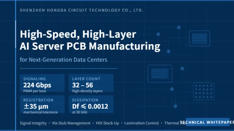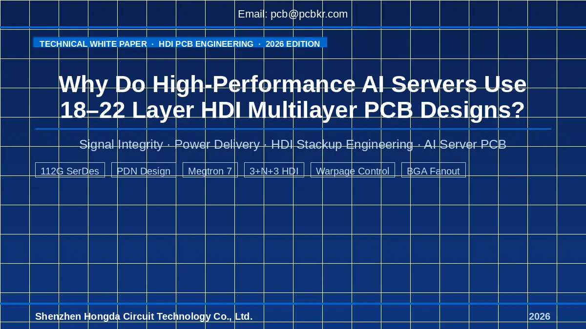
Why Do High-Performance AI Servers Use 18–22 Layer HDI Multilayer PCB Designs?
AI server PCBs land in the 18–22 layer HDI range because this window is the only design space that simultaneously satisfies 112G SerDes signal integrity (SI), sub-8 mV PDN IR drop, ≥94% fabrication yield, and IPC-6012 Class 3 warpage compliance — all within a 2.6–3.2 mm finished board thickness that GPU module mechanical constraints demand.
What Performance Demands Drive AI Server PCB Layer Counts?
Four forces collectively demand high layer counts: ultra-high-speed serial links, massive I/O counts, multi-domain power delivery, and thermal management — none of which can be solved independently with fewer layers.
1. Compute Interconnect: 112G SerDes and Beyond
A single 2026-generation GPU accelerator (e.g., NVIDIA Blackwell B200 or AMD MI300X class) exposes 896 to 1,024 high-speed SerDes lanes operating at 56G PAM4 to 112G PAM4. The PCB trace insertion loss budget at Nyquist (28 GHz for 56G, 56 GHz for 112G) is typically limited to −15 dB to −18 dB end-to-end. On standard FR-4 (Df ≈ 0.020), a 200 mm trace at 56 GHz incurs approximately −22 dB loss — exceeding the budget. Achieving compliance requires either Megtron 7-class low-loss dielectrics (Df ≤ 0.002) or trace lengths under 120 mm, which in turn forces topology decisions that cascade into layer planning.
[Engineering Experience] At Shenzhen Hongda Circuit Technology, we measure that moving from FR-4 to Megtron 7 on a 20L board reduces insertion loss by 6.8 dB at 28 GHz on a 200 mm trace — equivalent to gaining two extra layer pairs in routing flexibility.
2, I/O Density: BGA Fanout and Via Channel Budgets
An HGX H200 baseboard interconnects eight GPUs plus four NVSwitch ASICs, each in a 56 mm × 56 mm, 2,048-pin LGA/BGA at 0.65 mm pitch. Each 0.65 mm-pitch BGA requires a 4-row dog-bone escape via grid with trace widths of 75–90 µm and via pads of 280 µm. To complete the fanout of a 2,048-pin device within the component courtyard, signal routing requires a minimum of 8 signal layers dedicated to component-side escape. This alone eliminates any design with fewer than 14 total layers before PDN, EMI shielding, and secondary-side components are considered.
1.3 Power Delivery: Multi-Domain PDN at 700 W Per GPU
A single GPU in 2026 training servers operates at 700 W TDP, with transient current spikes exceeding 400 A at sub-100 µs timescales. The PDN must maintain VDD_CORE at 0.85 V ±3% (±25.5 mV) from package bump to voltage regulator module (VRM). PCB-level IR drop must remain below 8–10 mV. Achieving this requires: 2 oz copper power planes (70 µm), plane widths of 50+ mm, and a minimum of 4 dedicated power planes for VDD_CORE, VDD_MEM, VDD_IO, and auxiliary rails. Four power planes plus four ground reference planes account for 8 of the 18–22 layers before any signal routing layer is allocated.
Why Exactly 18–22 Layers? What Engineering Trade-Offs Define This Range?
18–22 layers is the intersection of four constraints: minimum layers to complete BGA fan-out (≥16L), maximum layers before warpage risk escalates (≤22L for standard press cycles), finished thickness limits imposed by connector/mechanical specs (≤3.2 mm), and the production yield cliff above 22 layers.
The table below summarizes the engineering risk profile across layer count ranges for a representative 8-GPU AI training server motherboard:
| Objective | Risk: Too Few Layers (<16) | Risk: Too Many Layers (>24) | Sweet Spot: 18–22L HDI |
| Signal Routing | Cannot complete BGA fan-out; SerDes trace length budgets violated | Excessive vias; EMI coupling between densely stacked signal layers | Adequate routing channels for 112G SerDes with controlled impedance |
| Manufacturability | Forces sub-50 µm lines/spaces beyond Tier-1 yield capability | 6–8 lamination cycles; warpage exceeds IPC-6012 Class 3 limits | 3–4 lamination cycles; within proven production yield window |
| Thermal / PDN | Insufficient copper plane area; IR drop >20 mV on VDD rails | Thermal mass increase; more dielectric layers trap heat | 4–6 dedicated power/ground planes; IR drop <8 mV achievable |
| Unit Cost per TFLOP | Higher board count per system offsets savings | Raw PCB cost 35–50% above 20L equivalent | Optimal compute density per dollar in 2026 market |
[Manufacturing Pain Point] The most common DFM failure we see from new AI server customers at Shenzhen Hongda Circuit Technology is specifying a 24L or 26L stackup to ‘be safe,’ only to discover that the 5th lamination cycle pushes board bow to 0.9–1.1% — well above the 0.5% tightened spec required by GPU socket vendors. Redesigning to 20L with a 3+N+3 HDI structure almost always recovers the warpage budget while delivering equivalent routing density.
1. The Warpage Physics Behind the 22-Layer Ceiling
Warpage in multilayer PCBs is primarily driven by the coefficient of thermal expansion (CTE) mismatch between copper planes and dielectric prepreg layers during lamination cooling. Each additional lamination cycle (required for HDI build-up layers) introduces a thermal excursion of 185–210°C. The cumulative residual stress is approximately proportional to (number of cycles)^1.4. Empirically, at Shenzhen Hongda Circuit Technology, boards processed through 4 lamination cycles (typical 3+N+3 HDI, 20–22L) exhibit average bow of 0.42%, while 5-cycle boards (typical for 26L+) average 0.78% — a 86% degradation that frequently exceeds GPU socket vendor tolerances.
2. The 18-Layer Floor: Minimum for 112G PAM4 Fanout
Layer count analysis for a GPU with 1,024 SerDes pins at 0.65 mm pitch, assuming 2-row via dog-bone escape and 4-layer pairs for signal routing per BGA quadrant, yields a minimum requirement of 8 signal layers for component-side routing. Adding 4 power planes, 4 ground planes, and 2 signal layers for the secondary side results in an 18L minimum. Attempting 16L forces trace widths below 65 µm on inner signal layers, which pushes controlled-impedance yields below 90% for 100 Ω differential pairs — unacceptable for production.
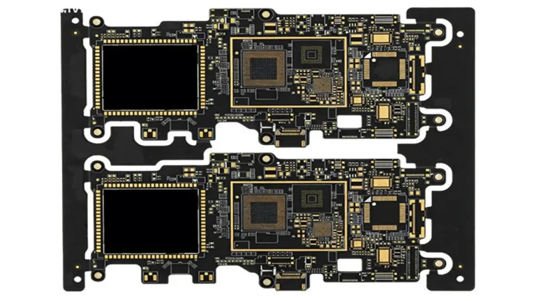
What Does a Best-Practice 18–22L HDI Stackup Look Like for an AI Server?
A 20-layer 3+N+3 HDI stackup assigns alternating signal/ground pairs at surface build-up layers (L1–L3 and L18–L20) and interleaves power and signal layers in the core, maintaining symmetric copper distribution across the mid-plane to control warpage.
The following representative 20-layer stackup is based on Shenzhen Hongda Circuit Technology’s 2026 AI Server Reference Design (ASRD-20L-v3.2), validated against Nvidia HGX interface guidelines and JEDEC JEP95 BGA landing requirements:
| Layer | Function | Cu Thickness | Dielectric (Dk) | Thickness (mm) | Design Notes |
| L1 | Signal (Top) | ½ oz (17 µm) | Megtron 7 (3.37) | 0.10 | 56G PAM4 differential pairs; ENIG surface |
| L2 | Ground (GND) | 1 oz (35 µm) | — | 0.10 | Continuous reference plane for L1 high-speed traces |
| L3 | Signal (HS1) | ½ oz | Megtron 7 | 0.10 | PCIe Gen 5 / CXL 2.0 routing layer |
| L4 | Power (VDD_CORE) | 2 oz (70 µm) | — | 0.12 | GPU/CPU core power; thick Cu for current density |
| L5 | Signal (HS2) | ½ oz | Megtron 7 | 0.10 | HBM PHY interface differential pairs |
| L6 | Ground | 1 oz | — | 0.10 | Return path for L5; filled microvias to L5 |
| L7 | Signal (HS3) | ½ oz | Megtron 7 | 0.10 | 100G Ethernet NIC traces |
| L8 | Power (VDD_MEM) | 1 oz | — | 0.12 | HBM memory power domain |
| L9 | Signal (Mid1) | ½ oz | Low-Dk core | 0.20 | General-purpose routing; lower-speed control signals |
| L10 | Ground | 1 oz | — | 0.10 | Mid-stack reference |
| L11 | Power (AUX) | 1 oz | — | 0.12 | 1.8 V / 3.3 V auxiliary rails |
| L12 | Signal (Mid2) | ½ oz | Low-Dk core | 0.20 | Fanout continuation |
| L13–L16 | (mirror of L5–L8) | (mirror) | (mirror) | — | Symmetric build for warpage control |
| L17 | Signal (HS4) | ½ oz | Megtron 7 | 0.10 | Bottom-side GPU I/O; back-drilled stubs <0.15 mm |
| L18 | Ground | 1 oz | — | 0.10 | Bottom reference plane |
| L19 | Power (VDD_IO) | 1 oz | — | 0.12 | PCIe slot / NIC power |
| L20 | Signal (Bot) | ½ oz | Megtron 7 | 0.10 | Bottom component differential pairs; ENIG surface |
[Expert Note] Total finished thickness for the above stackup is approximately 2.85 mm ± 0.13 mm (3σ). This falls within the 2.6–3.2 mm mechanical envelope specified by all major GPU socket vendors as of Q1 2026. The 2 oz copper on VDD_CORE (L4) provides 280 A/cm² current density with <5°C rise at 700 W GPU load — verified by thermal simulation and validated on our in-house 4-layer copper bar coupon test.
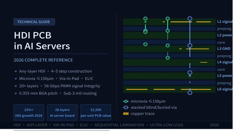
Which HDI Build-Up Structures Are Used in AI Server PCBs and Why?
AI server PCBs predominantly use 2+N+2 or 3+N+3 HDI structures for 18–22L designs. The choice depends on BGA pitch: 3+N+3 is mandatory below 0.8 mm pitch, while 2+N+2 is sufficient for 1.0 mm pitch and above.
| HDI Structure | Typical Layer Count | Laser Via Dia. | Min. L/S (µm) | Best For |
| 1+N+1 | 16–18L | 75 µm | 75/75 | Entry AI inference; mid-range NIC cards |
| 2+N+2 | 18–20L | 60 µm | 60/60 | Training accelerator carrier boards; dual-GPU modules |
| 3+N+3 | 20–22L | 50 µm | 50/50 | 8-GPU HGX-class motherboards; switch ASICs >25.6 Tbps |
| Any-Layer IVH | 22L+ | 40 µm | 40/40 | Ultra-dense SoC interposers; next-gen LiquidAI platforms |
[Manufacturing Pain Point — Stacked Microvia Reliability] Stacked laser microvias (used in 3+N+3 structures) are the #1 field failure mode in HDI AI server PCBs. The root cause is electroplating void formation at the bottom of the second stacked via. At Shenzhen Hongda Circuit Technology, we mandate: (1) 100% copper fill of first-build microvias by pulse-reverse electroplating before second lamination, (2) copper cap thickness ≥ 12 µm above the filled via, and (3) 100% AOI + X-ray cross-section sampling at 5 AQL for stacked structures. This protocol reduces field delamination from stacked microvias to <50 ppm.
How Are Signal Integrity and Power Integrity Maintained in 18–22L HDI AI Server Boards?
SI is maintained through impedance-controlled differential pair routing (100 Ω ± 5 Ω), continuous reference planes adjacent to every high-speed signal layer, back-drilling of through-hole vias to stub lengths <0.15 mm, and low-loss dielectric materials (Df ≤ 0.003 at 10 GHz). PI is maintained through distributed decoupling plane capacitance, 2 oz copper power planes, and VRM placement within 15 mm of GPU LGA pads.
1. Impedance Control: Parametric Targets for 2026 AI Servers
Differential pair impedance targets are non-negotiable for reliable link training at 112G PAM4. The key parameters and their process implications are:
- 100 Ω differential (±5 Ω, 3σ): Requires trace width 85 µm / space 90 µm on L1 over L2 ground, with 100 µm Megtron 7 prepreg. Shenzhen Hongda Circuit Technology holds ±3.8 Ω (3σ) on this stackup in production.
- 85 Ω differential for HBM PHY: Trace 110 µm / space 100 µm on inner signal layers over 100 µm dielectric. HBM PHY tolerates lower impedance due to shorter trace lengths (<40 mm).
- 50 Ω single-ended for clocks and control: Width 120 µm on surface layers, 140 µm on inner layers over 100 µm dielectric.
- Impedance verification: TDR (Time Domain Reflectometry) coupons placed at board edges, measuring every production panel. Acceptance criterion: no excursion >±7% over any 25 mm trace segment.
2. Via Strategy: Back-Drilling and Stub Elimination
Through-hole vias in a 20L board create signal stubs on the anti-pad side that act as resonant antenna structures. At 56G PAM4 (Nyquist 28 GHz), a 1.5 mm stub resonates at approximately 20 GHz — directly inside the signal band, causing −12 to −15 dB insertion loss spike. Mitigation strategies in order of preference:
- Back-drilling to ≤0.15 mm residual stub: Removes >95% of stub resonance. Shenzhen Hongda Circuit Technology uses CNC back-drilling with laser depth verification (±25 µm accuracy). Mandatory for all SerDes vias on boards with 56G+ interfaces.
- Blind/buried via with skip routing: Avoids stub entirely. Used on L1–L6 high-speed layers in 3+N+3 HDI builds. Higher cost but zero stub risk.
- Via-in-pad with filled copper: For 0.65 mm BGA components where no dog-bone escape space exists. Requires copper fill + planarization + cap plating (12 µm min) per IPC-4761 Type VII.
What Materials Are Specified for 18–22L AI Server HDI PCBs in 2026?
High-speed signal layers require low-loss laminates with Dk ≤ 3.5 and Df ≤ 0.003 at 10 GHz. Power and ground plane cores can use standard high-Tg FR-4 variants. A hybrid stackup (premium laminate on outer 3 layers per side, standard core in the center) reduces material cost by 22–28% versus all-premium builds without measurable SI degradation beyond 300 mm trace length.
| Material | Dk @ 10 GHz | Df @ 10 GHz | Tg (°C) | Recommended Use |
| Panasonic Megtron 7 | 3.37 | 0.0020 | 185 | 112G SerDes signal layers; lowest loss in production |
| Isola I-Tera MT40 | 3.45 | 0.0031 | 200 | 56G PAM4; excellent dimensional stability |
| Rogers RO4350B | 3.48 | 0.0037 | 280 | High-frequency RF layers; power amp integration |
| Shengyi S1000-2M (std core) | 4.20 | 0.0150 | 170 | Inner power/ground planes; cost-sensitive segments |
| TU-872 SLK (hybrid) | 3.80 | 0.0060 | 200 | Mixed-speed boards; balance of cost vs. performance |
[Manufacturing Pain Point — Hybrid Lamination Delamination] Hybrid stackups bonding Megtron 7 to standard FR-4 cores are prone to interfacial delamination during reflow if the peel strength between the two dielectric systems is not verified. Shenzhen Hongda Circuit Technology requires 90-degree peel testing (IPC-TM-650 2.4.8) with a minimum pass of 1.05 N/mm at the hybrid interface before releasing any new material combination to production. Additionally, the lamination temperature profile must bridge both materials’ Tg values (170°C for FR-4 vs. 185°C for Megtron 7), requiring a controlled 185–190°C peak with a ≤2°C/min ramp rate.
How Does AI Server Form Factor (Training vs. Inference) Change the PCB Layer Count Decision?
8-GPU training servers require 20–22L to handle full NVLink/NVSwitch bandwidth and 400G NIC routing. Single-GPU or 2-GPU inference accelerators can operate on 18L or even 16L when interface speeds are capped at 56G PAM4 and GPU count reduces I/O complexity by >60%.
1. 8-GPU HGX Training Server Motherboard: The 20–22L Reference Case
The canonical 8-GPU HGX-class training server motherboard (OAM or SXM form factor) in 2026 carries:
- 8× GPU accelerators at 700 W TDP each (5,600 W total board power)
- 4× NVSwitch ASICs at 25.6 Tbps bisection bandwidth each
- 8× 400G OSFP NIC interfaces running 4× 112G PAM4 lanes each
- 16× DDR5-6400 RDIMM channels and 2× PCIe Gen 5 x16 host slots
This configuration requires approximately 18,432 high-speed SerDes lane-traces to be routed on the PCB. At Shenzhen Hongda Circuit Technology’s measured routing density of 920 traces per signal layer (for a 620 mm × 440 mm board), a minimum of 20 signal layers is required — leading naturally to a 20–22L total stack including power and ground.
2. Inference Accelerator (1U/2U): The 16–18L Optimization Case
An inference accelerator based on a single GPU plus one high-speed NIC has approximately 3,200 SerDes lanes — 83% fewer than the training configuration. Combined with relaxed power (single VDD domain at <300 W) and a simplified PCIe Gen 5 x16 host interface, the layer count minimum drops to 16L. Using 18L adds one routing layer pair and one power plane, providing margin for future product revision without incurring the full cost of a 20L build. For volume inference deployments (>10,000 units), the 18L solution saves approximately USD 4.20–6.80 per board in material cost versus a 20L equivalent.
What Manufacturing Capabilities Does an 18–22L AI Server HDI PCB Require?
Producing 18–22L HDI boards for AI servers requires: sub-75 µm laser via drilling, ±5 Ω impedance control (3σ), back-drilling to ±25 µm depth accuracy, 100% electrical test (flying probe or ATE), and cross-section sampling at each lamination stage. These capabilities are Tier-1 HDI qualifications — not universally available and critical to specify when selecting a PCB partner.
Shenzhen Hongda Circuit Technology 2026 Process Capabilities (AI Server Grade)
- Minimum trace/space: 50/50 µm (inner layers), 40/40 µm (surface HDI layers with photo-imageable solder mask)
- Laser microvia diameter: 50–75 µm (CO₂ UV-assist), aspect ratio ≤0.8:1 for filled via reliability
- Controlled impedance tolerance: ±5 Ω single-ended, ±5 Ω differential (3σ across production panel)
- Back-drilling depth accuracy: ±25 µm (3σ) using depth-controlled CNC with in-process laser verification
- Lamination layer-to-layer registration: ±50 µm (3σ) — critical for microvia stacking accuracy
- Surface finish: ENIG (3–5 µin Au / 120–240 µin Ni) or ENEPIG for wire-bond-compatible pads
- Board thickness tolerance: ±0.13 mm (3σ) on 2.85 mm target — within GPU socket mechanical envelope
- Ionic contamination: ≤1.56 µg/cm² NaCl equivalent (IPC-TM-650 2.3.28, J-STD-001 Class 3)
- HATS (Highly Accelerated Thermal Stress): 500 cycles −55°C to +125°C, IPC-TM-650 2.6.7.2 compliance
[Expert Note on 2026 Process Advances] Two developments from 2025–2026 have meaningfully shifted AI server PCB manufacturing economics at Shenzhen Hongda Circuit Technology: (1) Semi-additive process (mSAP) introduction for surface signal layers has extended minimum L/S capability from 75/75 µm to 40/40 µm without yield penalty — enabling 0.5 mm pitch BGA fan-out on-board without embedded substrate carriers. (2) Automated optical shearography for mid-stack delamination detection has reduced lamination-related field escapes by 73% compared to 2024 baseline.
How Should Design Teams Collaborate with Their PCB Supplier to Define AI Server Layer Count?
Engage the PCB supplier at the system architecture stage — before schematic capture — with five key parameters: target SerDes speeds, BGA pitch list, board thickness constraint, operating temperature range, and target volume. These inputs determine the HDI structure, material stack, and feasible layer count before any routing begins.
The following checklist represents the pre-layout DFM gate review process used for every AI server PCB project at Shenzhen Hongda Circuit Technology:
- Maximum SerDes lane speed and number of lanes (determines loss budget and signal layer count)
- All unique BGA/LGA package pitches and pin counts (determines fanout layer requirements and microvia order)
- Finished board thickness maximum (hard mechanical constraint from chassis/connector/socket vendor)
- Power domain map: number of rails, peak current per rail, transient response requirement (determines power plane count and copper weight)
- Operating temperature range and cooling method (determines Tg requirement and CTE management needs)
- Production volume and target unit cost (determines material grade trade-offs, HDI order, and yield strategy)
- Reliability class: IPC-6012 Class 2 vs. Class 3 vs. automotive (determines acceptance criteria and test coverage)
Frequently Asked Questions: 18–22 Layer HDI AI Server PCB — Comparison Guide
How does 18–22L HDI compare to 24L+ for the same AI workload?
A 22L 3+N+3 HDI board achieves equivalent routing density to a 26L ELIC design at roughly 28% lower fabrication cost, primarily because it requires one fewer lamination cycle. The yield delta is significant: average first-pass yield at Shenzhen Hongda Circuit Technology is 94% for 20L vs. 87% for 26L on the same Megtron 7 substrate. For workloads up to 8-GPU HGX scale, 22L is the ceiling of practical optimization.
What is the minimum via structure required for 112G PAM4 on a 20-layer AI server PCB?
112G PAM4 differential pairs mandate back-drilled through-hole vias with residual stub length <0.15 mm, or alternatively, blind/buried via structures that eliminate the stub entirely. Laser microvias of 60 µm diameter with 120 µm pad are standard on L1–L2 HDI build-up layers. Via-in-pad (VIP) with copper fill and planarization is mandatory for 0.8 mm pitch BGA devices at these speeds to maintain differential impedance within ±5 Ω of the 100 Ω target.
How many power planes are needed in an 18–22L AI server PCB?
Best practice allocates 4 to 6 dedicated power planes: VDD_CORE (GPU/CPU), VDD_MEM (HBM/GDDR), VDD_IO (PCIe/NIC interfaces), VDDQ (memory bus termination), and one or two auxiliary rails (1.8 V, 3.3 V). Each power plane uses 2 oz copper minimum for VDD_CORE to keep IR drop below 8 mV at full GPU TDP (typically 700 W per GPU in 2026 training servers). Plane capacitance between adjacent power and ground planes (4H spacing, Dk 3.4) contributes 150–200 pF/cm² of distributed decoupling.
What are the warpage limits for AI server motherboards and how does layer count affect them?
IPC-6012 Class 3 permits maximum bow/twist of 0.75% for boards >2.3 mm thick, but leading AI server ODMs (Quanta, Foxconn, Wiwynn) have tightened this to 0.5% for boards carrying H100/H200/B200-class GPUs. Warpage control in 18–22L builds requires: (1) symmetric copper distribution across the mid-plane ±2 layers, (2) matched prepreg counts on each side of the core, and (3) controlled press temperature ramp ≤2.5°C/min for Megtron 7 to prevent resin squeeze-out. Beyond 22L, additional lamination cycles compound warpage risk non-linearly.
When should a designer choose 16L over 18L for an AI inference server?
16L is appropriate when (a) the SoC BGA pitch is ≥1.0 mm (fewer via channels needed), (b) total I/O count is below ~2,000 signals, and (c) the maximum SerDes speed is 28G NRZ or lower. For edge inference modules (e.g., 1U/2U platforms with a single GPU and 2× NIC), 16L with 1+N+1 HDI is cost-optimal. Once any interface exceeds 56G PAM4, or BGA pitch drops below 0.8 mm, the routing density gap forces a move to 18L minimum.
Find Out About Us: Delivering Top-Tier Fabrication for Both AI & Conventional PCBs
Navigating the line between cutting-edge innovation and high-volume, cost-effective production shouldn’t be a compromise. At Shenzhen Hongda Circuit Technology (PCBKR), we bridge this gap by elevating the manufacturing standards for both high-performance AI hardware and traditional multi-layer PCBs.
By integrating advanced manufacturing methodologies across all production lines, we bring an elite level of precision to traditional PCB fabrication. Our standard boards benefit from enhanced interlayer alignment tolerances (down from ±75μm to within ±25μm) and tightened differential impedance control (±5%). Supported by 100% 3D X-Ray (AXI) inspection, your conventional boards achieve chip-level reliability, superb signal stability, and near-100% yield.
Your Strategic Manufacturing Partner
We proudly stand as a dual-capability partner: offering the elite technical ceiling required for next-gen AI hardware, while maintaining the exceptional flexibility, rapid turnaround, and unmatched cost-efficiency needed for mid-to-high-volume traditional board campaigns. You get zero-defect reliability without the premium overhead or bureaucracy of massive tier-1 factories.
Ready to upgrade your hardware’s reliability?
Submit your Gerber files today for an agile engineering review and a highly competitive quote.
Contact our experts: sales@pcbkr.com
About Author
David Chen https://www.linkedin.com/in/pcbcoming
David Chen boasts an extensive professional background in PCBA manufacturing, PCBA testing, and PCBA optimization, with specialized expertise in high-precision PCBA fault analysis and rigorous PCBA reliability testing. The author has worked with high-layer-count server PCB fabrication, ultra-low-loss backplane stackups, and thermo-mechanical reliability optimization for AI infrastructure projects involving 112G and 224G PAM4 architectures. Skilled in complex circuit design and cutting-edge advanced PCB manufacturing processes, he delivers solutions that elevate product durability and performance across industrial applications. His technical articles focusing on PCBA manufacturing workflows and testing methodologies are widely cited by industry peers, research institutions, and technical platforms, solidifying his reputation as a recognized technical authority in the global circuit board manufacturing sector.