The Ultimate Guide to Multilayer PCB Stackup Design & Advanced Manufacturing Technology (2026 Edition)
The global printed circuit board industry is entering a defining era. From AI server infrastructure to next-generation automotive electronics, demand for precision multilayer PCB fabrication has never been more acute. At Shenzhen Hongda Circuit Technology Co., Ltd., we manufacture high-density interconnect (HDI) boards, controlled-impedance multilayer PCBs, and advanced rigid-flex assemblies for customers across North America, Europe, and Asia. This technical guide brings together our engineering expertise with the most significant PCB manufacturing innovations of 2026.
Whether you are an OEM engineer evaluating stackup configurations, a procurement manager benchmarking PCB fabrication capabilities, or a hardware designer navigating the shift to high-speed SerDes interfaces, this resource is built for you.
Table of Contents
- Introduction: The Era of High-Speed Multilayer Electronics
- 1. Why Multilayer PCB Stackup Design Is the Foundation of Modern Electronics
- 1.1 The DFM Gap Between Design and PCB Fabrication
- 2. Standard Multilayer PCB Stackup Configurations: 4-Layer, 6-Layer, and 8-Layer
- 2.1 4-Layer PCB Stackup – Cost-Performance Baseline
- 2.2 6-Layer PCB Stackup – Mainstream for AI Hardware
- 2.3 8-Layer PCB Stackup – AI Servers and High-Speed Backplanes
- 3. Impedance Control in PCB Manufacturing: Fundamentals and Practice
- 3.1 Variables That Determine Trace Impedance
- 3.2 Dielectric Material Selection for High-Speed Applications
- 3.3 Copper Thickness Trade-offs in Controlled Impedance PCBs
- 4. HDI PCB Technology and Microvia Design: 2026 Advancements
- 4.1 What Defines HDI PCB Manufacturing
- 4.2 Via Structure Selection for High-Speed Multilayer PCBs
- 5. EMI Reduction Through Stackup Engineering and Plane Management
- 5.1 Reference Plane Continuity and Return Current Paths
- 5.2 Layer Pairing for Power Delivery Noise Suppression
- 5.3 Symmetrical Stackup Design for Warpage Control
- 6. 2026 PCB Manufacturing Technology: Key Industry Advances
- 6.1 AI-Driven Process Automation in PCB Fabrication
- 6.2 Advanced Materials for High-Frequency Manufacturing
- 6.3 Rigid-Flex PCB Manufacturing for Space-Constrained Applications
- 6.4 Sustainable PCB Manufacturing Practices
- 7. Practical Stackup Design Workflow for Engineers (Step-by-Step)
- 8. Common PCB Stackup and Fabrication Mistakes to Avoid
- 9. Shenzhen Hongda Circuit Technology Co., Ltd. – Manufacturing Capabilities
- 10. Conclusion: Choosing the Right Multilayer PCB Manufacturing Partner
1. Why Multilayer PCB Stackup Design Is the Foundation of Modern Electronics
Every high-performance electronic system traces its signal integrity, power delivery, and electromagnetic compliance back to one decision made early in the design process: the PCB stackup. A stackup is not simply a layer count—it is the engineered arrangement of conductive and dielectric layers that determines impedance, crosstalk suppression, return current pathways, and thermal performance.
Stackup errors are expensive. A 10 Gbps differential pair routed across a split reference plane can exhibit more than 10% impedance deviation, degrading eye diagrams and causing system-level failures that take weeks to diagnose. In 2026, as PCIe Gen 5, DDR5, and 112 Gbps PAM4 SerDes become mainstream, the engineering cost of a poorly designed stackup is measured not just in board respins but in delayed product launches.
1.1 The DFM Gap Between Design and PCB Fabrication
One of the most persistent challenges in multilayer PCB manufacturing is the gap between what engineers design and what factories can reliably produce. Shenzhen Hongda Circuit Technology Co., Ltd. addresses this through early DFM (Design for Manufacturability) review—evaluating impedance tolerance, via structures, copper balance, and material choices before a single panel enters fabrication.
Common DFM failure points include:
- Non-symmetrical stackup causing board warpage during lamination.
- Impedance targets specified without accounting for copper thickness tolerance.
- High-speed traces routed on outer microstrip layers rather than inner stripline layers, increasing radiation and insertion loss.
- Missing impedance coupons on production panels, leaving no traceability for impedance verification.
2. Standard Multilayer PCB Stackup Configurations: 4-Layer, 6-Layer, and 8-Layer
Selecting the correct layer count is the first structural decision in multilayer PCB design. Layer count affects cost, signal integrity, EMI performance, and manufacturing complexity. Below are the three configurations most commonly produced at our facility, with engineering guidance on when each is appropriate.
2.1 4-Layer PCB Stackup – Cost-Performance Baseline
The 4-layer stackup remains the workhorse of industrial and embedded electronics. A standard configuration places signal layers on L1 (Top) and L4 (Bottom), with a ground plane on L2 and a power plane on L3.
Key engineering considerations for 4-layer designs:
- L1 must have an uninterrupted GND reference on L2 to maintain controlled impedance on surface microstrip traces.
- Power plane splits on L3 must not interrupt GND return paths for signals crossing different power domains.
- EMI control is more challenging than in higher-layer-count designs; component placement and decoupling discipline are critical.
Appropriate applications include low-speed AI edge modules, industrial control boards, and power management circuits where signal frequencies remain below 3 Gbps.
2.2 6-Layer PCB Stackup – Mainstream for AI Hardware
The 6-layer stackup represents the most common configuration for modern AI hardware, including GPU carrier boards, network switches, and memory modules. A well-designed 6-layer PCB provides dual reference planes for inner signal layers, enabling stripline routing with excellent crosstalk suppression and lower radiation than microstrip.
Recommended 6-layer sequence:
- L1: High-speed signal (Microstrip, top side)
- L2: Ground plane
- L3: Inner signal (Stripline, high-speed routing)
- L4: Power plane
- L5: Ground plane
- L6: Signal (Bottom side)
This arrangement sandwiches the most critical high-speed traces on L3 between two reference planes, minimizing near-end crosstalk (NEXT) and far-end crosstalk (FEXT). The adjacent GND-Power pair on L4–L5 creates a distributed plane capacitance that stabilizes the power delivery network (PDN).
2.3 8-Layer PCB Stackup – AI Servers and High-Speed Backplanes
The 8-layer multilayer PCB is the entry point for serious AI server infrastructure, PCIe Gen 4 and Gen 5 add-in cards, and 100G+ switching boards. All high-speed signal routing in an 8-layer design should be confined to inner stripline layers.
Example 8-layer configuration:
- L1: Signal – Microstrip (lower-priority nets, power management signals)
- L2: Ground plane
- L3: Signal – Stripline (high-speed SerDes, DDR)
- L4: Power plane
- L5: Power or signal (secondary high-speed)
- L6: Signal – Stripline (high-speed SerDes)
- L7: Ground plane
- L8: Signal – Microstrip (lower-priority nets)
Ground planes on L2 and L7 create a symmetrical, low-radiation structure. The symmetry is not merely aesthetic: asymmetrical copper distribution causes differential thermal expansion during reflow, resulting in warpage that directly affects solder joint reliability.
3. Impedance Control in PCB Manufacturing: Fundamentals and Practice
Controlled impedance is the most technically demanding requirement in multilayer PCB fabrication. A PCB with a specified impedance of 50 Ω on a single-ended trace or 100 Ω differential must be fabricated within a defined tolerance—typically ±10% for standard production and ±5% for advanced applications.
3.1 Variables That Determine Trace Impedance
Four physical parameters govern trace impedance in any layer stack:
- Dielectric thickness (h): The distance between the trace and its reference plane. Thinner dielectric results in lower impedance.
- Copper thickness (t): Affects the effective trace width after etching. Heavier copper reduces effective impedance.
- Trace width (w): Wider traces have lower impedance.
- Dielectric constant (Dk): Higher Dk materials reduce impedance and slow signal propagation velocity.
The interaction between these variables is why stackup definition must be done in collaboration with the PCB manufacturer before layout begins. Changes made after routing is complete often require full rerouting of controlled-impedance nets.
3.2 Dielectric Material Selection for High-Speed Applications
FR4—the industry standard for decades—has a Dk of approximately 4.2 to 4.5 and a dissipation factor (Df) of 0.020 or higher. For signals below 3 Gbps, FR4 performs adequately. Above 10 Gbps, FR4’s insertion loss per inch becomes unacceptable, and low-loss materials are required.
At Shenzhen Hongda Circuit Technology Co., Ltd., we work with the following dielectric classes:
- Standard FR4: Suitable for 4-layer and 6-layer designs up to 3 Gbps.
- Mid-loss materials (Df ≈ 0.010): Suitable for 6 to 10 Gbps applications.
- Low-loss materials (Megtron 6, Tachyon 100G, Df < 0.005): Required for 10 Gbps and above, including PCIe Gen 5 and 112 Gbps PAM4 SerDes.
Material selection is not a cost optimization variable—it is a system reliability decision. An AI accelerator board using FR4 at 25 Gbps will exhibit channel losses that no equalization can recover.
3.3 Copper Thickness Trade-offs in Controlled Impedance PCBs
Copper thickness is specified in ounces (oz), where 1 oz equals approximately 35 µm. The choice of copper weight affects both impedance controllability and fabrication yield.
- 0.5 oz copper on inner signal layers: Preferred for high-speed controlled impedance. Thinner copper is more uniformly etched, reducing impedance variation across the panel.
- 1 oz copper: Acceptable for moderate speeds and outer signal layers.
- 2 oz and heavier: Reserved for power planes and thermal management layers. Thick copper on signal layers creates significant etch undercut, making precise impedance control difficult.
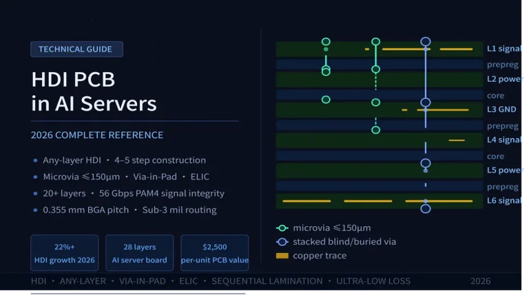
4. HDI PCB Technology and Microvia Design: 2026 Advancements
High-Density Interconnect (HDI) PCB technology has moved from a premium niche to a mainstream requirement across consumer electronics, automotive ADAS systems, and AI edge hardware. In 2026, HDI and ultra-HDI designs represent one of the fastest-growing segments in PCB manufacturing.
4.1 What Defines HDI PCB Manufacturing
HDI PCBs are characterized by:
- Microvias with diameters of 0.1 mm or smaller, enabling via-in-pad designs for fine-pitch BGAs.
- Trace widths and spaces of 75 µm / 75 µm (3 mil / 3 mil) or finer.
- Sequential lamination build-up processes (1+N+1, 2+N+2, and higher orders).
- Filled and capped vias for reliable BGA escape routing on 0.4 mm and 0.3 mm pitch packages.
The move toward ultra-HDI—with trace widths below 50 µm—is driven by the growing footprint of advanced packaging: chiplet designs, fan-out wafer-level packages (FOWLP), and CoWoS substrates all require board-level routing capability that approaches traditional IC substrate densities.
4.2 Via Structure Selection for High-Speed Multilayer PCBs
Via selection in a multilayer PCB has direct consequences for signal integrity at high speeds. The three primary via types each have distinct performance and cost profiles:
- Through-hole vias (PTH): Lowest cost, but introduce via stubs that create resonance nulls in the frequency response. At 10 Gbps and above, backdrilling is required to remove stubs and restore channel margin.
- Blind vias: Connect surface layers to internal layers without penetrating the full board thickness. Ideal for surface BGA escapes while eliminating stub effects.
- Buried vias: Connect internal layers to internal layers, invisible from the board surface. Used in dense HDI designs where surface via density would otherwise limit routing.
Backdrilling—controlled-depth mechanical drilling to remove unused via barrels—is now standard practice in our facility for any design targeting 10 Gbps or higher channel speeds.
5. EMI Reduction Through Stackup Engineering and Plane Management
Electromagnetic interference (EMI) compliance failures are among the most costly setbacks in hardware development. A board that fails radiated emissions testing late in the certification process requires both a hardware revision and a retest—typically adding six to twelve weeks and substantial cost to a product launch. Stackup-level EMI mitigation is far more effective and economical than post-layout EMI suppression.
5.1 Reference Plane Continuity and Return Current Paths
Every high-speed signal current has an equal and opposite return current flowing in the nearest reference plane. When the reference plane is split by a power domain boundary, a slot, or a connector keepout, the return current is forced to detour around the discontinuity. This detour increases the current loop area, directly increasing radiated emissions.
The engineering rule is absolute: no high-speed trace may cross a reference plane split. Layout teams must verify this during design review, not as a post-routing check.
5.2 Layer Pairing for Power Delivery Noise Suppression
Adjacent power and ground planes form a distributed planar capacitor. In a 6-layer stackup with L4 (Power) adjacent to L5 (GND), the effective capacitance per unit area is inversely proportional to the dielectric thickness between the planes. Specifying thin core material—0.1 mm rather than 0.2 mm—between power and ground planes doubles the distributed decoupling capacitance, reducing PDN impedance across the frequency range that matters most for processor core power delivery.
5.3 Symmetrical Stackup Design for Warpage Control
A stackup must be symmetrical about its center plane—not just in layer count, but in dielectric thickness, prepreg type, and copper weight distribution. Any asymmetry creates differential thermal expansion coefficients between the upper and lower halves of the board during lamination and reflow. The result is a curved board that causes assembly yield problems and, in severe cases, mechanical stress on BGA solder joints leading to field failures.
6. 2026 PCB Manufacturing Technology: Key Industry Advances
The PCB industry is undergoing accelerated transformation in 2026, driven by the infrastructure requirements of AI data centers, autonomous vehicles, and 5G/6G radio hardware. Several manufacturing technology developments are directly relevant to engineering decisions made today.
6.1 AI-Driven Process Automation in PCB Fabrication
AI-powered inspection and process control systems are now deployed throughout leading PCB manufacturing facilities. Automated optical inspection (AOI) systems trained on defect libraries of millions of images catch dimensional deviations invisible to conventional threshold-based systems. In-process impedance measurement on test coupons, correlated with dielectric and copper thickness measurements from earlier process steps, enables real-time stackup parameter adjustment before boards are laminated.
At Shenzhen Hongda Circuit Technology Co., Ltd., our production lines incorporate closed-loop process control that links incoming material characterization (Dk/Df measurement, copper roughness profiling) with impedance modeling to predict and correct impedance deviations before they occur.
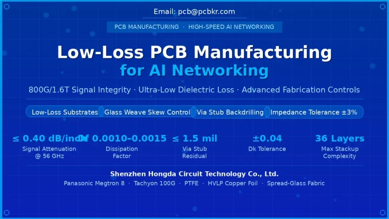
6.2 Advanced Materials for High-Frequency Manufacturing
Material science advancement in 2026 continues to extend the frequency range achievable in PCB-based systems. Key developments include:
- Ultra-low-loss laminates: Df values below 0.003 at 10 GHz, enabling PCB-based mm-wave antenna systems for 5G and 6G base stations.
- Thermally conductive dielectrics: Tc values above 2.0 W/m·K for high-power LED drivers and automotive power electronics where thermal management is as critical as signal performance.
- Halogen-free laminates: Meeting IEC 61249-2-21 requirements, now mandated by EU RoHS amendments and increasingly specified by automotive OEMs.
- Optimized copper-clad laminates: Controlled surface roughness profiles optimized for skin effect loss minimization at 56 Gbps and 112 Gbps PAM4 signaling speeds.
6.3 Rigid-Flex PCB Manufacturing for Space-Constrained Applications
Rigid-flex PCBs combining rigid multilayer sections with flexible polyimide interconnects eliminate connectors in weight-critical and space-constrained assemblies. In 2026, demand for rigid-flex PCBs is growing across wearable medical devices, aerospace avionics, and advanced driver assistance systems (ADAS) where connector reliability under vibration is a life-safety concern.
Manufacturing rigid-flex PCBs requires specialized tooling, controlled impedance design extended through the flex sections, and careful management of bend radius relative to copper weight and flex layer count. Shenzhen Hongda Circuit Technology Co., Ltd. maintains dedicated production capacity for rigid-flex assemblies up to 20 layers.
6.4 Sustainable PCB Manufacturing Practices
Environmental compliance is no longer a secondary consideration in PCB manufacturing procurement. Leading manufacturers in 2026 operate under ISO 14001 environmental management systems and have implemented:
- Closed-loop copper recovery from etch waste streams, recovering above 95% of process copper for recycling.
- Lead-free surface finishes (ENIG, ENEPIG, ImSn, ImAg) meeting RoHS Directive 2011/65/EU and its amendments.
- Reduction of VOC emissions in solder mask and surface treatment processes.
- Halogen-free laminate qualification for automotive and consumer electronics supply chains requiring IEC 61249 compliance.
7. Practical Stackup Design Workflow for Engineers (Step-by-Step)
Producing a manufacturable, high-performance multilayer PCB stackup requires a systematic workflow that engages both the design team and the PCB manufacturer from the earliest stages of a project. The following sequence is used by engineering teams working with Shenzhen Hongda Circuit Technology Co., Ltd.:
- Step 1 – Define Interface Requirements: Document all electrical interfaces: signal data rates, interface standards (PCIe Gen 5, USB4, DDR5, 100G Ethernet), impedance requirements (single-ended and differential), and current-carrying requirements for power rails. This specification drives every subsequent stackup decision.
- Step 2 – Select Dielectric Material: Match dielectric Dk and Df to the highest-frequency interface. Request material data sheets from your PCB manufacturer and verify that the Dk and Df values reflect measured behavior at the operating frequency, not the 1 MHz test frequency commonly cited in generic datasheets.
- Step 3 – Determine Layer Count and Plane Assignment: Assign ground and power planes based on the number of high-speed signal layers required. A useful heuristic: each high-speed signal layer requires an adjacent reference plane. The stackup should dedicate at least 40% of its layers to ground and power planes for designs above 10 Gbps.
- Step 4 – Calculate Impedance and Verify with Manufacturer: Use a field-solver tool (Polar Si9000, HyperLynx, Ansys SIwave) to calculate trace impedance for target widths and dielectric thicknesses. Submit the stackup to your PCB manufacturer for their impedance modeling, using their measured material parameters and process capability data. Request a stackup confirmation sheet with guaranteed impedance tolerances.
- Step 5 – Define Via Structures and Backdrilling Requirements: Specify via types, drill diameters, and backdrilling depth for all controlled-impedance via transitions. Include this information in the fabrication note on the stackup drawing. Omitting backdrilling requirements from fabrication documentation is a common cause of channel performance failures in production boards.
- Step 6 – Generate Stackup Drawing and DFM Checklist: Create a formal stackup drawing specifying each layer’s function, material, thickness, copper weight, and finished impedance targets. Include an impedance coupon specification for each impedance structure type. Submit for DFM review before releasing to fabrication.
8. Common PCB Stackup and Fabrication Mistakes to Avoid
Engineering experience at Shenzhen Hongda Circuit Technology Co., Ltd. has identified recurring design issues that result in fabrication re-spins, EMI failures, or signal integrity margin loss. The following represent the highest-frequency engineering errors in multilayer PCB design:
- Crossing split planes with high-speed signals: The most common EMI failure cause. No exceptions; reroute the trace or revise the plane split.
- Specifying impedance without accounting for copper thickness tolerance: An impedance target of ±5% requires understanding that ±0.5 oz copper weight variation translates directly to impedance deviation.
- Asymmetric stackup structures: Any stackup where the upper and lower halves differ in copper weight or dielectric thickness will warp during lamination. Symmetry must be verified before releasing the stackup.
- Routing high-speed signals on outer microstrip layers unnecessarily: Outer-layer microstrip trades isolation for ease of routing. Inner stripline layers provide better crosstalk suppression and lower radiation.
- Omitting impedance coupons from production panels: Without coupons, there is no way to verify that the fabricated boards meet impedance specifications. This is a fundamental process control requirement, not an optional extra.
- Releasing stackup to fabrication without DFM review: A stackup confirmed by both the design team and the manufacturer before layout begins eliminates the most expensive class of PCB design errors.
9. Shenzhen Hongda Circuit Technology Co., Ltd. – Manufacturing Capabilities
Shenzhen Hongda Circuit Technology Co., Ltd. is a professional PCB manufacturer based in Shenzhen, China, supplying multilayer PCBs, HDI boards, rigid-flex assemblies, and high-frequency PCBs to customers worldwide. Our manufacturing capabilities are aligned with the demands of AI hardware, telecommunications infrastructure, automotive electronics, and industrial automation.
Core manufacturing capabilities include:
- Multilayer PCBs from 2 to 40 layers.
- HDI build-up constructions including 1+N+1 and 2+N+2 sequential lamination.
- Controlled impedance fabrication with ±5% and ±10% tolerance classes.
- High-frequency PCBs using PTFE, Rogers, Megtron 6, and equivalent low-loss laminates.
- Rigid-flex PCBs up to 20 layers with UL-listed polyimide flex materials.
- Heavy copper PCBs up to 20 oz for power electronics and busbars.
- Surface finishes including ENIG, ENEPIG, HASL (lead-free), ImSn, ImAg, and OSP.
- IPC Class 2 and Class 3 workmanship certification.
- ISO 9001:2015, ISO 14001:2015, and IATF 16949 quality management.
Our engineering team is available for stackup consultation, DFM review, and impedance modeling prior to design release. We believe that the best PCB is one where manufacturing constraints are understood by the design team from day one, and that philosophy is embedded in every customer engagement at Shenzhen Hongda Circuit Technology Co., Ltd.
10. Conclusion: Choosing the Right Multilayer PCB Manufacturing Partner
The printed circuit board is simultaneously the most ubiquitous and most underappreciated component in modern electronics. Every technological breakthrough—AI inference at the edge, autonomous vehicle sensing systems, 5G base station radios—is enabled or constrained by the PCB that carries the signals between components.
In 2026, the gap between generic PCB fabrication and precision multilayer PCB manufacturing has widened. AI hardware, high-speed SerDes interfaces, and millimeter-wave RF systems require a manufacturing partner with deep materials knowledge, proven impedance control processes, and the engineering collaboration capability to bridge the DFM gap.
Shenzhen Hongda Circuit Technology Co., Ltd. was built to close that gap. From 4-layer industrial boards to 20-layer AI server backplanes, from standard FR4 to PTFE-based mm-wave antenna substrates, our manufacturing capability and engineering support are available to customers who demand more than a board house—and need a true PCB manufacturing partner.
Contact Shenzhen Hongda Circuit Technology Co., Ltd.
E-mail: sales@pcbkr.com
Location: Shenzhen, Guangdong, China
FAQs
What is your standard turnaround and DFM review process for high-speed AI server PCBs?
At Shenzhen Hongda Circuit Technology Co., Ltd., we close the DFM (Design for Manufacturability) gap by performing a rigorous pre-fabrication engineering review. Our team evaluates layer symmetry to prevent board warpage, verifies copper thickness tolerances against impedance targets, and ensures proper microvia and stripline configurations before panels enter production to eliminate costly re-spins.
What advanced materials do you support for 10 Gbps+ and high-frequency 2026 applications?
We support a wide array of advanced, high-performance dielectrics optimized for low insertion loss. While we process standard FR4 for designs under 3 Gbps, we specialize in mid-loss materials (Df ≈ 0.010) and low-loss/ultra-low-loss laminates (including Megtron 6, Tachyon 100G, and PTFE-based substrates with Df < 0.005) tailored for PCIe Gen 5, 112 Gbps PAM4 SerDes, and mm-wave antenna systems.
Can you meet tight controlled impedance tolerances for multi-layer and HDI boards?
Yes. We deliver controlled impedance fabrication within standard ±10% tolerances, as well as advanced ±5% precision tolerance classes required for high-speed AI infrastructure and telecommunications. We incorporate automated in-process impedance testing and mandatory impedance coupons on production panels to guarantee complete verification and traceability.
What are your manufacturing limits for high-density interconnect (HDI) and heavy copper PCBs?
Our core manufacturing capabilities are built to scale for high-end electronics. We fabricate multilayer PCBs up to 40 layers, support rigid-flex assemblies up to 20 layers, and deliver advanced HDI build-ups (including 1+N+1 and 2+N+2 lamination with microvias ≤ 0.1 mm and trace configurations down to 75 µm). Additionally, we manufacture heavy copper boards up to 20 oz for power electronics.
What quality management certifications and environmental standards does your factory hold?
Shenzhen Hongda Circuit Technology Co., Ltd. operates under strict globally recognized standards to ensure industrial compliance. We are certified in ISO 9001:2015, ISO 14001:2015, and IATF 16949 (automotive quality). Our production adheres to IPC Class 2 and Class 3 workmanship, utilizes RoHS-compliant lead-free finishes (ENIG, ENEPIG, ImSn, ImAg, OSP), and features closed-loop copper recycling systems.
About Author
David Chen https://www.linkedin.com/in/pcbcoming
David Chen boasts an extensive professional background in PCBA manufacturing, PCBA testing, and PCBA optimization, with specialized expertise in high-precision PCBA fault analysis and rigorous PCBA reliability testing. The author has worked with high-layer-count server PCB fabrication, ultra-low-loss backplane stackups, and thermo-mechanical reliability optimization for AI infrastructure projects involving 112G and 224G PAM4 architectures. Skilled in complex circuit design and cutting-edge advanced PCB manufacturing processes, he delivers solutions that elevate product durability and performance across industrial applications. His technical articles focusing on PCBA manufacturing workflows and testing methodologies are widely cited by industry peers, research institutions, and technical platforms, solidifying his reputation as a recognized technical authority in the global circuit board manufacturing sector.