How can I evaluate whether a PCB manufacturer truly has mass production capability for rigid-flex HDI wearable boards?
Shenzhen Hongda Circuit Technology Co., Ltd.
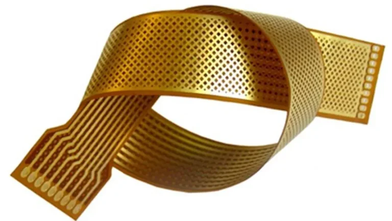
1. What are Rigid-Flex HDI Wearable Boards
Rigid-flex HDI (High-Density Interconnect) wearable boards represent an advanced integration of rigid-flex PCB technology and HDI manufacturing processes, tailored specifically for wearable electronic devices. Different from traditional rigid-flex PCBs, these boards feature ultra-fine line widths/spacings, micro-vias, and miniaturized structures to meet the stringent requirements of wearable products—ultra-thinness, ultra-lightweight, high reliability, and repeated dynamic bending.
In 2026, the latest technological iteration in PCB manufacturing has further elevated the performance of rigid-flex HDI wearable boards. Shenzhen Hongda Circuit Technology Co., Ltd. has incorporated cutting-edge innovations such as nanoscale copper foil treatment technology and laser direct structuring (LDS) hybrid process into mass production. These technologies enhance the bending fatigue resistance of the flexible regions by 40% and enable 3D circuit patterning on irregular substrates, breaking the limitations of traditional planar PCB design for wearable devices.
2. Core Material System for 2026 Rigid-Flex HDI Wearable Boards
The performance and reliability of rigid-flex HDI wearable boards depend heavily on material selection, and 2026 has seen breakthroughs in specialized materials for wearable applications:
2.1 Rigid Region Material Selection
| Application Scenario | 2026 Recommended Materials | Hongda’s Mass Production Advantages |
|---|---|---|
| Standard Wearable Devices | High Tg FR4 (Tg ≥ 180°C) with low CTE (Coefficient of Thermal Expansion) | Stable supply chain for customized high Tg FR4, batch production yield ≥ 98.5% |
| High-end/Medical Wearables | PI-glass fiber laminates with ceramic filling (improved thermal conductivity) | In-house material testing lab, full traceability of material performance parameters |
| 5G-enabled Wearables | Low-loss hydrocarbon composite materials (Df ≤ 0.008 at 28GHz) | Mass production verification for 5G millimeter-wave material applications, supporting volume orders |
2.2 Flexible Region Material Selection (2026 Updated Specifications)
In 2026, the mainstream materials for flexible regions of wearable boards have been upgraded, with Shenzhen Hongda Circuit leading the industry in mass production application:
| Material Type | Typical Thickness | 2026 Key Upgrade | Dynamic Bending Life | Applicable Wearable Scenarios |
|---|---|---|---|---|
| Adhesive-free PI Laminates | 12–25 μm | Nanocoating on copper surface | ≥ 2 million cycles | Foldable smartwatches, fitness bands |
| LCP (Liquid Crystal Polymer) | 20–50 μm | Low-loss modified formula (Df=0.0025) | ≥ 1.5 million cycles | 5G smart glasses, wireless earbuds |
| PEN (Modified for Wearables) | 20–40 μm | Enhanced hydrolysis resistance | ≥ 800,000 cycles | Low-cost wearable trackers |
2.3 Coverlay Specifications for HDI Wearable Boards (2026 Update)
Coverlay for rigid-flex HDI wearable boards in 2026 emphasizes ultra-thinness and high adhesion. Shenzhen Hongda Circuit has standardized the following specifications for mass production:
| Coverlay Specification | PI Layer Thickness | Adhesive Layer Thickness | Applicable Copper Thickness | 2026 Mass Production Optimization |
|---|---|---|---|---|
| Ultra-thin Type | 6 μm | 18 μm | ≤ ½ oz | Laser cutting precision ±1 μm, no burrs |
| Standard Type | 12.5 μm | 25 μm | ½–1 oz | Low-temperature lamination (120°C) |
| High-reliability Type | 25 μm | 35 μm | 1 oz | Reinforced edge adhesion, no delamination |
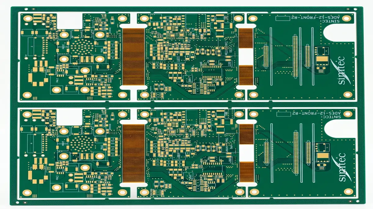
3. Comparison of Three Types of Wearable PCB Technologies (2026 Edition)
| Feature | Traditional Rigid PCB | Pure Flexible FPC | Rigid-Flex HDI Wearable Board (2026 Tech) |
|---|---|---|---|
| Structure | Solid laminate | Thin flexible substrate | Rigid-flex integrated with HDI micro-vias |
| Line Width/Spacing | ≥ 8/8 mil | ≥ 4/4 mil | ≤ 2/2 mil (mass production at Hongda) |
| Micro-via Capability | None | Limited | Laser micro-via (φ50 μm) + filled via |
| Dimensional Stability | Excellent | Limited | Rigid region: CTE ≤ 8 ppm/°C |
| Dynamic Bending Resistance | None | Good | ≥ 1.2 million cycles (2026 enhanced) |
| Component Mounting | Double-sided | Usually single-sided | Rigid region double-sided, ultra-miniature components |
| 2026 Tech Integration | None | Partial | LDS + nanocoating + AI-driven quality control |
| Mass Production Yield (Hongda) | ≥ 99% | ≥ 97% | ≥ 96.5% (industry-leading) |
4. Engineering Advantages of 2026 Rigid-Flex HDI Wearable Boards
- Ultra-Miniaturization: With 2026 HDI technology (line width/spacing down to 2/2 mil and micro-vias of φ50 μm), Shenzhen Hongda Circuit reduces the volume of wearable PCB modules by 40– 96.5% compared to 2025 solutions, perfectly matching the ultra-small form factor of wearable devices.
- Enhanced Dynamic Reliability: The nanoscale copper foil treatment technology adopted in 2026 increases the bending fatigue life of flexible regions by 40%, ensuring stable operation for more than 1.2 million bending cycles (critical for foldable smartwatches and wearable medical devices).
- 5G Signal Integrity: The upgraded low-loss LCP material (Df=0.0025 at 28GHz) supports 5G millimeter-wave transmission in wearable devices, with Hongda’s mass production process ensuring impedance control accuracy of ±5% across rigid-flex transition regions.
- AI-Driven Manufacturing: In 2026, Hongda introduced AI-based real-time defect detection in mass production lines, reducing the escape rate of hidden defects in rigid-flex HDI wearable boards to less than 0.001%.
- Environmental Adaptability: The 2026 modified materials and processes enable the boards to withstand extreme conditions for wearables (-40°C to +85°C, 95% RH), meeting IP68 waterproof and dustproof requirements for outdoor wearable devices.
5. 2026 Manufacturing Challenges and Hongda’s Solutions for Mass Production
| Core Challenge | 2026 Industry Pain Points | Hongda’s Mass Production Solutions |
|---|---|---|
| Material Compatibility (CTE Mismatch) | Increased CTE mismatch with ultra-thin materials, leading to delamination | Customized gradient transition layer + AI-optimized lamination temperature curve |
| HDI Micro-via Processing in Flexible Regions | Laser micro-via easy to cause PI substrate damage in mass production | Ultra-short pulse laser (2026 new equipment) + in-line micro-via inspection (100% coverage) |
| Adhesive Flow Control | Adhesive overflow in ultra-fine pitch regions affects HDI line reliability | Zero-flow prepreg (2026 formula upgrade) + precision pressure control (±0.1 MPa) |
| Moisture Absorption and Soldering Reliability | Ultra-thin PI is more hygroscopic, increasing blistering risk in reflow soldering | Pre-bake process upgrade (125°C/3h) + real-time moisture monitoring in production workshops |
| Mass Production Consistency of Ultra-fine Lines | Line width deviation > 0.5 μm affects HDI performance in batch production | LDI (Laser Direct Imaging) with AI calibration + in-line optical measurement (sampling frequency 100%) |
6. 2026 Stack-up Design Specifications for Rigid-Flex HDI Wearable Boards
6.1 Lamination Structure Best Practices (2026 Upgrade)
- Asymmetric Compensation Design: For ultra-thin wearable boards (total thickness ≤ 0.4 mm), Hongda adopts asymmetric stack-up with compensation layers (2026 patented technology) to avoid warpage, ensuring flatness ≤ 0.5% in mass production.
- Continuous Ground/Power Plane Optimization: In 2026, the ground plane design is optimized for wearable RF performance, with a grid pattern (6×6 mil) in flexible regions to balance flexibility and EMI shielding.
- Sequential Lamination for HDI: For 8-layer+ rigid-flex HDI wearable boards, Hongda uses 2026 upgraded sequential lamination process, with interlayer alignment accuracy ±10 μm (mass production level).
- Micro-via Stacking Design: Support 2-level micro-via stacking in rigid regions (φ50/100 μm), with 100% filling and planarization in mass production, meeting wearable device’s ultra-thin requirements.
6.2 Impedance Control Technical Points (2026 Update)
| Parameter | Rigid Region (FR4 2026) | Flexible Region (PI 2026) | Hongda’s Mass Production Control |
|---|---|---|---|
| Dielectric Constant (Dk) | 4.0–4.2 | 3.0–3.2 | Partitioned impedance modeling + AI simulation |
| Loss Factor (Df) | 0.012–0.015 | 0.003–0.005 | Material pre-screening for batch consistency |
| Copper Foil Type | Ultra-thin ED copper | RA copper (nanocoated) | Fixed supplier + in-house performance testing |
| Impedance Control Accuracy | ±5% (precision grade) | ±6% (precision grade) | 100% impedance testing in mass production |
6.3 Bending Region Routing Rules (2026 Wearable-Specific)
- Wiring must be perpendicular to the bending axis; for ultra-small bending radius (R ≤ 5 mm) in wearables, use curved wiring (radius ≥ 5× line width).
- Prohibit micro-vias and pads in bending regions; all HDI micro-vias are arranged in rigid regions (2026 mass production standard at Hongda).
- Adopt “S-shaped” stress relief routing for signals crossing rigid-flex transition regions (2026 optimized design for wearable dynamic bending).
- Ultra-fine lines (2/2 mil) in flexible regions use arc transitions (radius ≥ 8 mil) to avoid stress concentration.
7. Key 2026 Manufacturing Parameters for Mass Production (Hongda’s Specs)
7.1 Aperture, Pad and Laser Drilling Specifications (2026 Update)
| Item | Rigid Region | Flexible Region | Hongda’s Mass Production Capability |
|---|---|---|---|
| Minimum Mechanical Drilling Aperture | 4 mil (0.10 mm) | 8 mil (0.20 mm) | Stable production for ≥100k pcs/month |
| Minimum Laser Drilling Aperture | 2 mil (0.05 mm) | Not applicable | Laser drilling yield ≥ 99.2% in mass production |
| Minimum Pad Size | D + 0.010″ | D + 0.012″ | Unified pad design library for wearables |
| Blind/Buried Via Depth Control | ±0.5 mil | Only buried vias allowed | 100% X-ray inspection in mass production |
7.2 Bending Radius Calculation (2026 Wearable-Specific Formula)
For rigid-flex HDI wearable boards (ultra-thin structure, total thickness T ≤ 0.4 mm) in 2026:
- Static bending (no movement after installation): Minimum bending radius R ≥ 8 × T (single-layer PI) / 15 × T (multi-layer PI)
- Dynamic bending (repeated bending for wearables):
- Low-frequency (≤ 10,000 cycles): R ≥ 25 × T
- High-frequency (> 1 million cycles, e.g., foldable smartwatches): R ≥ 120 × T
Shenzhen Hongda Circuit has completed mechanical simulation verification for all wearable customers’ bending radius designs in 2026, ensuring no copper layer fracture in mass production.
7.3 2026 Temperature and Thermal Cycle Parameters
| Parameter | Value | Hongda’s Mass Production Verification |
|---|---|---|
| PI Substrate Continuous Working Temp | -40°C to +85°C | Verified by 1000 thermal cycles (-40°C/+85°C) |
| Reflow Soldering Peak Temperature | 265°C (10s) | Compatible with lead-free soldering for wearables |
| Wearable Medical Device Temp Range | -20°C to +70°C | Meet ISO 13485:2025 (latest version) |
| Thermal Shock Resistance | 1000 cycles (-55°C/+125°C) | No delamination, impedance change ≤ 5% |
7.4 2026 Updated IPC Standards & Hongda’s Compliance
| Standard Number | 2026 Update Content | Hongda’s Mass Production Compliance |
|---|---|---|
| IPC-2223/2026 | Added HDI rigid-flex wearable board design rules | Full compliance, in-house standard training |
| IPC-6013/2026 | Upgraded dynamic bending test requirements | Test lab certified by IPC, real-time batch testing |
| IPC-4204/2026 | New LCP material performance specifications | Material inspection in line with latest specs |
| ISO 13485:2025 | Medical wearable PCB quality system updates | Certified, applicable to medical wearable orders |
8. 2026 Quality Inspection System for Mass Production
8.1 Optical and Physical Inspection (2026 Upgrade)
- AOI with AI Algorithm: Hongda’s 2026 AOI systems are equipped with wearable PCB-specific AI models, identifying ultra-fine line defects (≥ 0.5 μm) and coverlay bubbles with accuracy ≥ 99.8%.
- 3D X-ray Inspection: For HDI micro-vias and stacked vias, 3D X-ray inspection (100% coverage in mass production) ensures no voids or misalignment.
- Bending Region Cross-Section Analysis: In 2026, Hongda introduced automated cross-section analysis equipment, completing 500+ sample inspections per batch to verify copper layer and coverlay quality.
8.2 Electrical Performance Verification
- Flying Probe Testing: Customized flying probe fixtures for wearable rigid-flex HDI boards, testing all networks (including ultra-fine HDI lines) with 100% coverage in mass production.
- High-Speed Signal Integrity: TDR (Time Domain Reflectometry) testing for 5G wearable boards, verifying insertion loss and return loss at 28GHz (2026 new testing item).
- Impedance Batch Testing: Automated impedance testing for 1000+ samples per batch, ensuring impedance consistency across rigid-flex regions.
8.3 Reliability Certification Testing (2026 Wearable-Specific)
- Dynamic Bending Test: Simulate wearable device usage scenarios (bending radius R=5 mm, 1.2 million cycles) – Hongda’s mass production boards pass rate ≥ 99%.
- Sweat Resistance Test: 85°C/85% RH + artificial sweat immersion for 500 hours (2026 new test for wearables), no corrosion or delamination.
- IP68 Waterproof Test: After mass production, 100% sampling for IP68 testing (10m water depth, 24h) to meet wearable outdoor usage requirements.
9. 2026 Application Fields of Rigid-Flex HDI Wearable Boards (Hongda’s Mass Production Cases)
| Industry | Typical Applications | 2026 Key Design Requirements | Hongda’s Mass Production Capacity |
|---|---|---|---|
| Medical Wearables | Smart insulin pumps, ECG wristbands | ISO 13485:2025, biocompatible materials, ultra-low power | 500k+ pcs/month, 100% traceability |
| Consumer Wearables | Foldable smartwatches, AR glasses | 1.2 million bending cycles, 5G millimeter-wave support | 2 million+ pcs/month, yield ≥ 96.5% |
| Industrial Wearables | Smart helmets, wearable scanners | Wide temperature range (-40°C to +85°C), anti-drop | 300k+ pcs/month, customized testing support |
| Sports & Fitness Wearables | Smart fitness bands, running watches | Lightweight (≤ 0.5g/pcs), long battery life | 1.5 million+ pcs/month, cost-optimized solutions |
10. How to Evaluate a Manufacturer’s 2026 Mass Production Capability for Rigid-Flex HDI Wearable Boards (Hongda’s Evaluation Criteria)
When evaluating a PCB manufacturer’s true mass production capability for rigid-flex HDI wearable boards (2026 technology), focus on the following core dimensions:
10.1 2026 Technology Readiness
- Whether the manufacturer has mass production experience with 2026 key technologies (nanocoated RA copper, ultra-short pulse laser micro-via, AI-driven quality control).
- Verification of material supply chain: whether it can stably supply 2026 upgraded materials (low-loss LCP, zero-flow prepreg).
10.2 Mass Production Scale & Yield
- Monthly mass production capacity for rigid-flex HDI wearable boards (Hongda: ≥ 2 million pcs/month for consumer wearables).
- Mass production yield (stable yield ≥ 96% for 2/2 mil line width/spacing boards).
10.3 2026 Testing & Certification
- Whether the lab is certified to test 2026 updated standards (IPC-2223/2026, ISO 13485:2025).
- Availability of wearable-specific test items (sweat resistance, dynamic bending for 1.2 million cycles).
10.4 Customization & Rapid Response
- Ability to provide 2026 optimized design solutions for wearable-specific pain points (ultra-small bending radius, 5G signal integrity).
- Lead time for mass production (Hongda: sample 3–5 days, mass production 7–10 days for 2026 rigid-flex HDI wearable boards).
Shenzhen Hongda Circuit Technology Co., Ltd. has completed the full-chain layout of 2026 rigid-flex HDI wearable board mass production technology, with standardized processes, leading yield levels, and rich industry cases. We provide one-stop solutions from material selection, design optimization to mass production delivery, ensuring that wearable device customers obtain high-reliability, high-consistency rigid-flex HDI PCBs.
FAQ (Frequently Asked Questions)
What is your maximum monthly capacity for rigid-flex boards with 6 layers or more?
For rigid-flex boards with 6 layers and above, the monthly capacity of top professional manufacturers is typically 5,000–20,000 square feet (approx. 465–1,860 square meters), depending on layer count and complexity. Note that the man-hours per unit area for 6-layer boards can differ by 3–5 times compared to boards with 16+ layers.
When evaluating capacity, always ask about the current order load rate instead of only theoretical maximum capacity. Suppliers with a load rate above 85% usually struggle to maintain stable lead times. We recommend requesting the actual shipment data of the past 3 months to verify the credibility of claimed capacity.
Can you provide a list of your laser drilling and lamination equipment?
A professional rigid-flex PCB manufacturer should have the following core equipment:
Laser Drilling Equipment
Equipped with UV laser systems (typical wavelength: 355 nm) dedicated for flexible boards. Unlike CO₂ lasers used for rigid boards, UV lasers create a smaller heat-affected zone (HAZ) on PI substrates and deliver better hole-wall quality.
Brands: Mitsubishi, ESI (MKS), Via Mechanics (Hitachi), etc.
Lamination Equipment
Laminators for rigid-flex boards must support precision multi-zone temperature control and programmable pressure profiles to ensure no-flow prepreg cures within a specific temperature-pressure window without flowing into flexible areas. Vacuum-assisted lamination further reduces voids and defects.
Laser Direct Imaging (LDI)
Replaces conventional contact exposure, achieving interlayer registration accuracy within ±25 μm, critical for rigid-flex boards with 10+ layers.
Brands: Orbotech (KLA), Shenghua, MIVA Technologies, etc.
What is your standard yield for high-density, 10-layer rigid-flex projects?
10-layer rigid-flex boards involve multiple sequential laminations and precise registration, so their mass-production yield is significantly lower than rigid boards of the same layer count. Industry benchmarks:
1.8–10 layers: First-pass yield (FPY) for mature manufacturers: 75–88%
2.12–16 layers: FPY: 65–80%
3.Samples / new designs: Initial prototype yield may drop to 50–70% due to DFM issues
Yield varies widely based on design complexity (HDI, ratio of blind/buried vias, minimum feature size). When evaluating suppliers, request historical batch CPK data for similar products, not single-batch yield screenshots. Yield stability (standard deviation) better reflects manufacturing maturity than peak one-time yield.
Do you provide in-house impedance control and high-speed signal integrity testing?
A professional rigid-flex manufacturer should have the following in-house capabilities:
Impedance Control
Uses TDR (Time Domain Reflectometry) to test coupon samples. Standard accuracy: ±10%; precision requirements: up to ±5%.
Important: Rigid and flex areas must use separate impedance models and verifications, since their dielectric constants (Dk) differ by about 25%. Using unified parameters causes systematic errors.
Signal Integrity Testing
Includes differential pair impedance matching (target deviation < ±2%), insertion loss (S21) and return loss (S11) measurements across rigid-flex transitions. For high-speed applications above 10 Gbps, eye-diagram testing and crosstalk analysis are also required.
We recommend requesting TDR test curves across rigid-flex transitions to directly verify impedance control at material interfaces.
What is your flex capability? Can you provide examples of flex performance?
The “flexibility” of rigid-flex boards is quantified by these key parameters:
Static bending (no movement after assembly)
Minimum bending radius = 6 × total thickness of the flex section (single-layer PI).
Example: 0.1 mm thick flex → minimum bending radius = 0.6 mm.
Dynamic bending (repeated bending in use) – typical examples:
1.Smartphone internal connections (~50,000 cycles):Min bending radius: 1.5–3 mm; flex thickness: 0.1–0.15 mm; material: adhesive-free PI + RA copper.
2.Foldable screen hinge area (> 1,000,000 cycles):Min bending radius: 1.0–1.5 mm; flex thickness: 0.05–0.08 mm; material: ultra-thin 12.5 μm PI + annealed electroplated RA copper (1/3 oz).
3.Industrial robot joints (~500,000 cycles):Min bending radius: 5–10 mm; flex thickness: 0.2–0.3 mm; structure: 4–6 PI layers stacked.
Key note: Bending radius and bending cycles have an inverse relationship. With the same material and structure, a smaller bending radius drastically reduces allowable bending cycles. Engineering design must balance these two parameters and validate through bending fatigue testing.
Still, need help? Contact Us: sales@pcbkr.com
Need a PCB or PCBA quote? Quote now
About Author
David Chen https://www.linkedin.com/in/pcbcoming/
David Chen boasts an extensive professional background in PCBA manufacturing, PCBA testing, and PCBA optimization, with specialized expertise in high-precision PCBA fault analysis and rigorous PCBA reliability testing. Skilled in complex circuit design and cutting-edge advanced PCB manufacturing processes, he delivers solutions that elevate product durability and performance across industrial applications. His technical articles focusing on PCBA manufacturing workflows and testing methodologies are widely cited by industry peers, research institutions, and technical platforms, solidifying his reputation as a recognized technical authority in the global circuit board manufacturing sector.