Why Do AI Server PCBs Require More Testing?
AI server PCBs require far more testing because they operate under extreme current density, ultra-high-speed PAM4 signaling, continuous thermal cycling, and synchronized multi-GPU workloads. A microscopic PCB defect that would be harmless in traditional servers can trigger AI training collapse, GPU desynchronization, packet retransmission storms, or catastrophic cluster instability.
Why Are AI Server PCB Failure Risks Much Higher Than Traditional Server Boards?
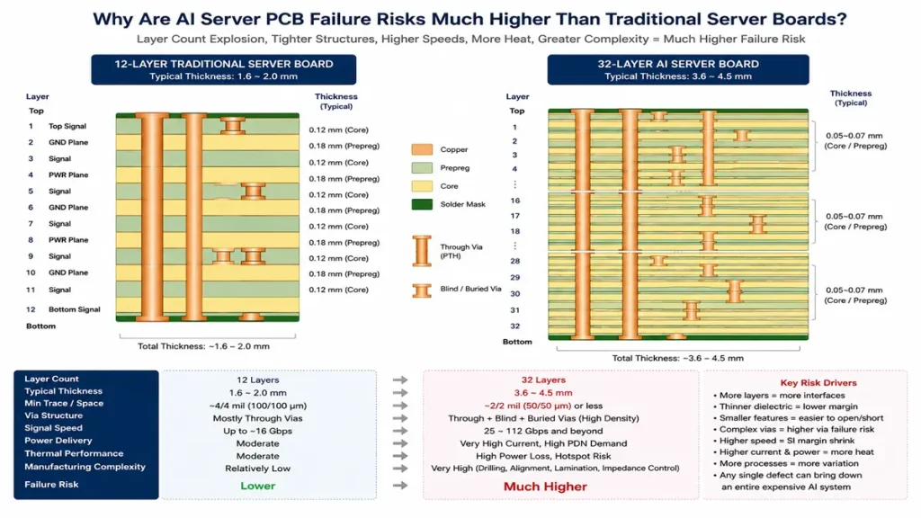
AI-Server-PCB-12-Layer-vs-32-Layer-Stackup-Failure-Risk-Comparison
AI server PCBs combine ultra-high current delivery, 112G/224G PAM4 signaling, heavy copper structures, and complex multilayer architectures into a single platform, dramatically shrinking manufacturing tolerances and amplifying hidden reliability risks.
Traditional enterprise server boards typically operate at:
| Parameter | Traditional Server PCB | AI Server PCB |
|---|---|---|
| Signaling Speed | 10G–25G NRZ | 112G/224G PAM4 |
| PCB Layer Count | 12–16 Layers | 20–36 Layers |
| GPU/CPU Power | 250–350W | 700–1200W |
| Rack Power Density | 10–20kW | 80–150kW |
| Via Aspect Ratio | 6:1–8:1 | 10:1–16:1 |
| Copper Structure | 1 oz | 2–4 oz mixed copper |
| Thermal Stress Level | Moderate | Continuous high-delta cycling |
In practical AI infrastructure, PCB defects no longer remain isolated electrical failures. They rapidly propagate into:
- GPU synchronization instability
- NVLink retransmission
- PCIe CRC errors
- Tensor retraining loops
- VRM thermal runaway
- Distributed training interruption
During one multilayer AI accelerator tray validation project evaluated by our engineering team, channels near the panel center exhibited intermittent eye collapse despite impedance coupons remaining within specification. Root-cause analysis later identified localized dielectric thickness variation caused by non-uniform lamination pressure across a 24-layer ultra-large panel.
That manufacturing phenomenon is becoming increasingly common in AI server PCB production because AI platforms now operate extremely close to physical signal integrity limits.
Why Does 112G/224G PAM4 Signaling Require Much More PCB Validation?
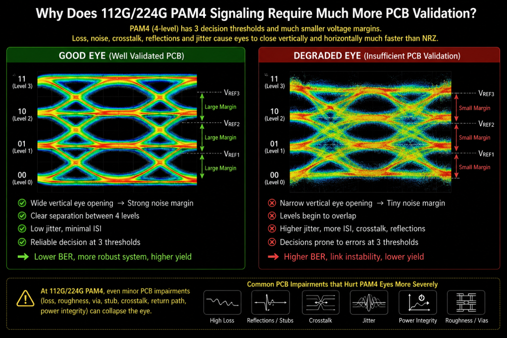
pam4-eye-diagram-good-vs-degraded-112g-pcb-validation
At 112G/224G PAM4 speeds, microscopic impedance discontinuities, via resonance, resin variation, and dielectric instability can immediately destabilize AI communication channels.
At 112G PAM4:
- Unit Interval (UI) ≈ 8.9 ps
- Typical insertion loss budget < 28 dB
- Differential impedance target:
- 85Ω ±5%
- Backdrill residual stub tolerance:
- often below 6 mils
A backdrill depth deviation of only:
- 4–6 mils
may introduce sufficient resonance energy to generate:
- deterministic jitter
- eye closure
- BER degradation
- equalization instability
This is why advanced AI server PCB validation now includes:
- S-parameter extraction
- VNA insertion loss verification
- TDR impedance scanning
- PAM4 eye diagram analysis
- NEXT/FEXT crosstalk validation
- backdrill residue inspection
Manufacturing pain point:
AI server PCB panels frequently exceed:
- 600 mm platform dimensions
- 30-layer stackups
- low-loss/high-speed hybrid materials
Under these conditions, resin flow imbalance during lamination can create dielectric thickness variation of:
- ±8–12 µm
That small geometric variation alone can shift differential impedance beyond acceptable PAM4 margins.
In one real manufacturing evaluation involving a 32-layer AI training board, our engineers observed that channels positioned close to large copper power regions consistently exhibited higher insertion loss compared with channels located near balanced signal regions. The root cause was uneven resin starvation caused by asymmetric copper distribution during multilayer pressing.
Traditional PCB inspection methods passed the board electrically, yet real AI traffic triggered intermittent retraining failure after prolonged thermal loading.
This is exactly why modern AI server PCB validation increasingly resembles telecom backplane qualification rather than traditional enterprise motherboard testing.
Why Does AI Power Delivery Testing Become Extremely Aggressive?
Modern AI GPUs generate massive transient current spikes that expose tiny resistance variation, copper imbalance, and via reliability weaknesses inside the PCB structure.
A single high-end AI accelerator can exceed:
- 900–1200A transient current demand
during tensor processing bursts.
Even:
- 0.15 mΩ localized resistance deviation
can generate enormous localized thermal energy.
P=I2R
At 900A:
- additional localized heat ≈ 121.5W
inside an extremely confined copper region.
This creates:
- localized Joule heating
- via barrel expansion
- copper fatigue accumulation
- solder joint degradation
- thermal runaway concentration
Manufacturing pain point:
AI server boards increasingly combine:
- 0.5 oz signal layers
- 3 oz power planes
- embedded copper structures
- ultra-heavy VRM copper regions
This mixed-copper architecture generates highly uneven thermal expansion during lead-free reflow cycles.
In one AI compute motherboard project investigated during thermal stress testing, our reliability engineers observed that stacked microvia fatigue occurred preferentially near copper transition boundaries where thermal expansion coefficients changed abruptly between dense power regions and fine-pitch signal escape routing.
The failure mechanism was not immediate electrical breakdown. Instead, the PCB gradually accumulated thermo-mechanical fatigue after:
- 300–500 thermal cycles
- repeated GPU load transitions
- continuous 24/7 AI operation
This explains why AI server validation increasingly requires:
- high-current injection testing
- thermal shock cycling
- IR thermal imaging
- dynamic PDN impedance mapping
- transient current waveform analysis
According to senior power integrity engineers working on modern AI accelerator systems:
“Many AI server boards no longer fail electrically first. They fail mechanically after surviving repeated power transients.”
Why Is Thermal Reliability Testing Far More Important in AI Server PCBs?
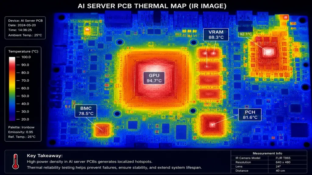
ai-server-pcb-ir-thermal-map-gpu-hotspot-94c
AI workloads create continuous high-temperature operation that accelerates resin aging, copper fatigue, microvia cracking, and long-term interconnect degradation.
Traditional server platforms often operate at:
- 35–55°C average board temperatures
Modern AI GPU platforms may sustain:
- 75–95°C localized hotspot temperatures
- 24/7 full-load training operation
- continuous thermal ramp cycling
Under these conditions, PCB materials experience accelerated:
- Tg fatigue
- resin decomposition
- pad cratering
- solder fatigue
- CAF growth
- microvia cracking
Therefore, AI server PCB testing increasingly includes:
| Reliability Test | AI Server Requirement |
|---|---|
| IST | Mandatory |
| Thermal Cycling | Extended |
| HAST | Frequently Required |
| CAF Resistance | High Priority |
| X-Ray Void Inspection | Critical |
| Thermal Warp Analysis | Continuous |
Manufacturing pain point:
Large AI boards exceeding:
- 3.5–5.5 mm thickness
often develop severe thermal warpage after repeated thermal stress.
During one high-density GPU tray validation project, our engineering team observed PCB warpage exceeding:
- 0.75%
during sustained AI thermal loading.
That distortion gradually altered BGA coplanarity near GPU corners and eventually produced intermittent socket instability after approximately:
- 9–11 hours
of continuous AI training.
Traditional burn-in tests failed to reproduce the problem because the thermal ramp rate was insufficiently aggressive.
Only long-duration AI workload simulation exposed the failure mechanism.
This is why hyperscale AI infrastructure companies increasingly demand:
- workload-level validation
- real AI traffic simulation
- long-duration thermal aging
- dynamic telemetry monitoring
instead of relying solely on ICT or flying-probe inspection.
Why Do AI Server PCBs Require More Advanced Via Reliability Testing?
AI server PCBs rely heavily on stacked microvias, deep backdrilled structures, and ultra-high aspect ratio vias that become mechanically vulnerable under combined thermal and electrical stress.
Modern AI server boards may contain:
- tens of thousands of vias
- stacked HDI structures
- deep backdrilled vias
- ultra-dense BGA escape routing
Critical via failure risks include:
- barrel cracking
- plating voids
- corner separation
- resin recession
- conductive anodic filament growth
AI server via structures frequently reach:
| Via Parameter | Traditional Server | AI Server |
|---|---|---|
| Mechanical Via Aspect Ratio | 6:1–8:1 | 10:1–16:1 |
| Laser Via Stack Depth | 1–2 levels | 3–5 levels |
| Drill Tolerance Window | Moderate | Extremely Tight |
Manufacturing pain point:
As PCB thickness increases beyond:
- 4 mm
drill wander becomes increasingly nonlinear.
That creates:
- annular ring reduction
- impedance asymmetry
- plating thickness inconsistency
- signal resonance instability
In one AI backplane manufacturing analysis performed by our process engineering group, excessive drill deviation caused localized plating weakness near ultra-thick copper transition areas. The defect passed AOI inspection but later failed during accelerated interconnect stress testing after repeated thermal expansion cycles.
This explains why advanced AI PCB validation increasingly depends on:
- microsection analysis
- X-ray tomography
- SEM cross-section inspection
- IST accelerated cycling
- via reliability characterization
Why Do AI Clusters Require System-Level PCB Validation Instead of Simple Board Testing?
Many AI infrastructure failures only appear during synchronized multi-GPU operation under real thermal and electrical loading conditions.
A PCB may successfully pass:
- AOI
- flying probe
- ICT
- impedance inspection
- continuity verification
yet still fail during real AI training.
Why?
Because distributed AI systems generate synchronized:
- thermal saturation
- GPU current spikes
- simultaneous SerDes activity
- VRM load transitions
- network congestion bursts
that conventional PCB testing never reproduces.
In one 16-GPU AI cluster investigation evaluated during system-level validation, intermittent training failure repeatedly appeared after approximately:
- 36 hours
despite all standalone PCB inspections passing successfully.
Root-cause analysis later identified temperature-dependent impedance drift near high-speed connector regions operating under sustained thermal saturation.
The defect only emerged during:
- full GPU synchronization
- maximum network traffic
- elevated thermal equilibrium
This is precisely why modern AI server manufacturers increasingly require:
- cluster-level validation
- AI workload simulation
- BER telemetry monitoring
- long-duration stress testing
- real-time thermal logging
Why Is AI Server PCB Testing Becoming Similar to Aerospace and Telecom Validation?
AI hardware now operates near physical reliability limits where microscopic manufacturing variation can trigger large-scale operational instability.
Modern AI server platforms combine:
- telecom-grade signal integrity
- aerospace-level reliability expectations
- automotive-style thermal cycling
- hyperscale uptime requirements
Failure costs are enormous.
A single unstable AI cluster may waste:
- thousands of GPU hours
- megawatt-scale power consumption
- weeks of AI model training time
That economic impact fundamentally changes PCB testing philosophy.
Today, the engineering question is no longer:
“Does the PCB electrically function?”
Instead, modern AI infrastructure manufacturers ask:
“Can this PCB survive continuous hyperscale AI operation for years without instability?”
That is a completely different reliability standard.
FAQs
How does the signaling speed of AI server PCBs compare to traditional server PCBs, and why does it matter?
Traditional server PCBs operate at 10G–25G NRZ signaling, while AI server PCBs push to 112G/224G PAM4. At these extreme speeds, the unit interval shrinks to roughly 8.9 ps, meaning even a backdrill depth deviation of just 4–6 mils can introduce enough resonance energy to cause eye closure, jitter, and BER degradation — failures that would be completely inconsequential at lower traditional speeds.
How do power delivery demands differ between traditional and AI server PCBs?
Traditional server GPUs/CPUs draw 250–350W, whereas AI accelerators can demand 700–1200W with transient current spikes exceeding 900–1200A during tensor processing bursts. Even a localized resistance deviation of just 0.15 mΩ can generate over 121W of concentrated heat at those current levels — a power integrity challenge that simply doesn’t exist at traditional server scales.
How does thermal stress compare between the two platforms?
Traditional servers typically run at 35–55°C average board temperatures with moderate thermal cycling. AI servers sustain 75–95°C localized hotspots under continuous 24/7 full-load operation. This accelerates resin aging, microvia cracking, CAF growth, and copper fatigue in ways that conventional burn-in tests fail to reproduce — requiring instead long-duration AI workload simulation.
How do via structures and their associated risks differ?
Traditional server PCBs use mechanical via aspect ratios of 6:1–8:1 with laser via stacks of 1–2 levels. AI server PCBs require aspect ratios of 10:1–16:1 and stacked HDI structures reaching 3–5 levels deep. As board thickness exceeds 4mm, drill wander becomes increasingly nonlinear, causing annular ring reduction and plating inconsistency — defects that can pass AOI inspection yet fail later under accelerated thermal cycling.
How does the validation philosophy for AI server PCBs differ from traditional board testing?
Traditional PCB testing asks simply, “Does the board electrically function?” — relying on AOI, flying probe, ICT, and continuity checks. AI server validation has evolved to ask, “Can this PCB survive continuous hyperscale AI operation for years?” This demands cluster-level testing under synchronized multi-GPU workloads, real AI traffic simulation, and long-duration thermal aging, because failures often only emerge after 36+ hours of full GPU synchronization — conditions that conventional testing never reproduces.
Using top-tier AI server PCB equipment to manufacture traditional PCBs delivers a strategic advantage: interlayer alignment tolerance shrinks from ±75μm to within ±25μm, and differential impedance control tightens to ±5%. Paired with 100% 3D X-Ray inspection, it grants conventional boards chip-level precision, superb signal stability, and near-100% yield.
Still, need help? Contact Us: sales@pcbkr.com
Need a PCB or PCBA quote? Quote now
About Author
David Chen https://www.linkedin.com/in/pcbcoming/
David Chen boasts an extensive professional background in PCBA manufacturing, PCBA testing, and PCBA optimization, with specialized expertise in high-precision PCBA fault analysis and rigorous PCBA reliability testing. Skilled in complex circuit design and cutting-edge advanced PCB manufacturing processes, he delivers solutions that elevate product durability and performance across industrial applications. His technical articles focusing on PCBA manufacturing workflows and testing methodologies are widely cited by industry peers, research institutions, and technical platforms, solidifying his reputation as a recognized technical authority in the global circuit board manufacturing sector.