How 224G PAM4 Changes AI Backplane PCB Design?
How 224G PAM4 Changes AI Backplane PCB Design?
The relentless rise of generative AI clusters has pushed data center architectures to their absolute physical limits, forcing a rapid transition toward 224G PAM4 PCB infrastructure. As next-generation AI servers demand unprecedented bandwidth to process massive LLMs (Large Language Models), the industry is moving away from 112G NRZ/PAM4 signaling, transforming the traditional 224G backplane into a highly complex, ultra-low-loss system requiring pioneering fabrication capabilities.
The Physics of 224G PAM4: Why Traditional PCB Design Fails
To understand how 224G PAM4 changes AI backplane PCB design, we must look at the signal behavior. At 224 Gbps per channel using PAM4 (Pulse Amplitude Modulation 4-Level), the Nyquist frequency climbs to an astonishing 56 GHz. At these extreme frequencies, traditional FR-4 or even standard low-loss megtron substrates act more like attenuators than conductors.
Key Transmission Challenges at 56 GHz Nyquist Frequency
- Severe Skin Effect: High-frequency electrons travel only on the outermost skin of the copper trace, drastically increasing conductor loss.
- Glass Weave Effect: The microscopic gaps between woven fiberglass and resin cause localized dielectric constant (Dk) variations, leading to phase skew between differential pairs.
- Via Resonance: Standard via stubs act as open-ended transmission lines, reflecting signals back and destroying the eye diagram.
Material Evolution: Extreme Low-Loss Substrates and Copper Foil
Designing a reliable 224G backplane requires an overhaul of the PCB material stackup. Standard high-speed materials cannot meet the strict insertion loss budgets required by AI hardware architectures.
| Parameter | 112G PAM4 Requirement | 224G PAM4 Requirement (Shenzhen Hongda 2026 Standard) |
|---|---|---|
| Dielectric Constant (Dk) | ≤ 3.5 | ≤ 3.0 (Utilizing Next-Gen Non-Woven Hydrocarbon Glass/Glass Core) |
| Dissipation Factor (Df) | ≤ 0.002 | ≤ 0.0010 – 0.0012 (Ultra-Low Loss Evolution) |
| Copper Foil Type | HVLP (Hyper Very Low Profile) | HVLP3 / Ultra-smooth profiles with Resins (Rz ≤ 0.55 μm) |
| Glass Cloth Style | 1067 / 1078 (Standard Mechanical) | 1015 / 1027 (Ultra-Thin Uniform Flat-Weave Fiber) |
To maintain signal integrity across long backplane reaches, materials like Panasonic Megtron 8 or Tachyon 100G are combined with ultra-smooth copper foils to mitigate the skin effect.
Advanced Layer Stackup & VIA Design for 224G Backplanes
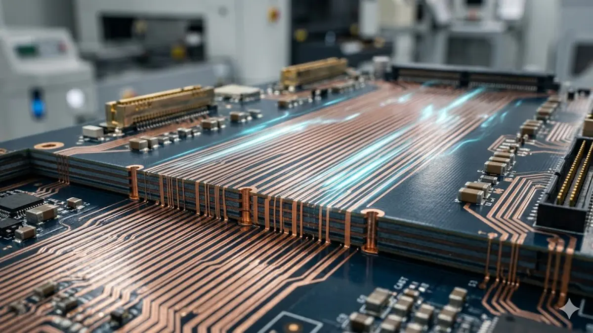
A typical AI backplane accommodating 224G lines often requires high-layer-count configurations, scaling anywhere from 24 to over 60 layers to isolate high-speed signals from power planes.
Structural Design Adaptations
- mSAP (Modified Semi-Additive Process): Traditional subtractive etching creates trapezoidal traces, which cause impedance discontinuities. Implementing mSAP allows for near-rectangular trace cross-sections, optimizing impedance control within ± 5%.
- Backdrilling Depth Control: For a 224G PAM4 PCB, any remaining via stub must be kept under 2 mil (50 μm). Advanced laser-controlled backdrilling or blind/buried via architectures are strictly mandatory to avoid signal resonance.
- Orthogonal Direct Connect: To eliminate the long trace lengths of traditional backplanes, AI architectures increasingly leverage orthogonal architectures where line cards and switch cards connect directly, minimizing the backplane trace length to the absolute minimum.
Real-World Case Study: 224G AI Cluster Hardware Deployment
blockquote> Project Target: High-Density AI Supercomputing Backplane
Layer Count: 48 Layers
Key Metric: Total insertion loss budget of < 30 dB at 56 GHz for a 10-inch channel length.
The Solution: By replacing standard HVLP copper with HVLP3 copper and utilizing a highly customized, ultra-low-loss resin system, the insertion loss was reduced from 3.2 dB/inch to 2.5 dB/inch. Combined with strict automated optical inspection (AOI) and time-domain reflectometry (TDR) testing during fabrication, the final 224G backplane achieved stable eye-opening metrics across all differential channels, validating the structural reliability of the AI cluster.
2026 Advanced Comparison FAQ (Technical Insights)
How does Shenzhen Hongda’s 2026 ultra-low-loss substrate handle the glass weave effect compared to standard 112G methods?
In standard 112G PAM4 production, relying on standard flat-weave glass cloths (like 1067) often allows localized Dk imbalances to introduce substantial phase skew at 28 GHz. For 224G PAM4 signaling running at 56 GHz Nyquist frequency, Shenzhen Hongda Circuit Technology Co., Ltd. adopts the 2026 advanced uniform non-woven substrate matrices and ultra-thin flat-weave 1015 glass cloths. This reduces dielectric constant variation across the board to less than ±0.04, successfully eliminating phase skew within critical differential lines.
What is the mechanical difference between standard backdrilling and Shenzhen Hongda’s 2026 laser-controlled depth drilling for 224G PAM4 PCBs?
Standard mechanical backdrilling typically yields a via stub tolerance of ±5 mil ($127\,\mu\text{m}$), which acts as a devastating resonator causing significant signal drop-outs at 56 GHz. In 2026, Shenzhen Hongda utilizes advanced laser-CCD depth-controlled backdrilling, shrinking the via stub tolerance to an elite ≤2 mil ($50\,\mu\text{m}$) threshold. This mechanical precision prevents stub resonance and keeps signal reflections below the strict -20dB limit required by AI OAM/UBB hardware layouts.
How do traditional subtractive etching and 2026 mSAP (Modified Semi-Additive Process) compare in high-speed impedance control?
Substrictive chemical etching creates a trapezoidal trace cross-section with an uneven etch factor, forcing impedance variations up to ±10%. For a high-frequency 224G PAM4 PCB, this discontinuity causes catastrophic signal attenuation. By executing a 2026-optimized mSAP workflow, Shenzhen Hongda flash-etches vertical trace walls to lock down trace tolerances to within ±5 μm, keeping impedance strictly within a tight ±5% window for flawless signal propagation.
Why can’t HVLP copper foils used in 112G backplanes support 224G backplane architectures, and what is the 2026 alternative?
While standard HVLP (Hyper Very Low Profile) copper foil profile roughness ($R_z \approx 1.2\,\mu\text{m}$) functions safely for 112G PAM4, the skin effect at 224G PAM4 shifts the entire signal path to the immediate outer skin of the conductor. At 56 GHz, this roughness induces immense conductor losses. Shenzhen Hongda’s 2026 stackups implement HVLP3 and treated ultra-smooth foils with an $R_z \le 0.55\,\mu\text{m}$, reducing skin-effect attenuation by up to 22% compared to last-generation layouts.
What reliability validation distinguishes a 2026 high-performance AI backplane from standard enterprise-grade server boards?
Enterprise server boards typically endure standard 500-hour Conductive Anodic Filamentation (CAF) testing and basic thermal cycling. However, high-density AI clusters operate continuously at elevated thermal states. Shenzhen Hongda Circuit Technology Co., Ltd. qualifies all 224G backplanes under an expanded 1000-hour CAF testing protocol (at 85°C / 85% RH) and utilizes 67 GHz Vector Network Analyzers (VNAs) for full-spectrum Insertion Loss and Crosstalk scanning, guaranteeing sustained operational lifetimes under strenuous AI training workloads.
Partnering for Next-Generation AI Hardware
Successfully deploying a 224G PAM4 PCB demands more than just premium materials—it requires deep engineering collaboration between the hardware designer and the fabrication plant. As a specialized manufacturer of high-end, multi-layer PCBs and precise assemblies, Shenzhen Hongda Circuit Technology Co., Ltd. delivers the manufacturing tolerance, material expertise, and advanced stackup capabilities necessary to bring your 224G hardware to life.
Using top-tier AI server PCB equipment to manufacture traditional PCBs delivers a strategic advantage: interlayer alignment tolerance shrinks from ±75μm to within ±25μm, and differential impedance control tightens to ±5%. Paired with 100% 3D X-Ray inspection, it grants conventional boards chip-level precision, superb signal stability, and near-100% yield.
Still, need help? Contact Us: sales@pcbkr.com
Need a PCB or PCBA quote? Quote now
About Author
David Chen https://www.linkedin.com/in/pcbcoming
David Chen boasts an extensive professional background in PCBA manufacturing, PCBA testing, and PCBA optimization, with specialized expertise in high-precision PCBA fault analysis and rigorous PCBA reliability testing. Skilled in complex circuit design and cutting-edge advanced PCB manufacturing processes, he delivers solutions that elevate product durability and performance across industrial applications. His technical articles focusing on PCBA manufacturing workflows and testing methodologies are widely cited by industry peers, research institutions, and technical platforms, solidifying his reputation as a recognized technical authority in the global circuit board manufacturing sector.