What Defines a Reliable AI Server PCB Manufacturer for NVIDIA GPU and GPU System Board Design?
ditiAs transmission frequencies scale up to 224G PAM4 and hardware designs migrate toward complex multi-GPU cluster architectures, traditional PCB fabrication boundaries are being pushed to their limits. A reliable GPU power-delivery and high-speed PCB manufacturer typically transitions from standard production to an advanced engineering-driven methodology. This requires managing high-layer-count stack-ups (24+ to 36+ layers), heavy-copper power distribution networks (PDN), sub-5% impedance tolerances, and advanced signal integrity verification prior to the physical tooling stage.
What are the Special PCB Requirements for High-Performance GPU Systems?
The Core Challenge: Next-generation GPU systems demand ultra-high-density interconnects (HDI), complex multi-layer stack-ups with high-aspect-ratio vias, and ultra-low-loss substrates engineered to mitigate severe insertion losses at 112G and 224G PAM4 frequencies. Simultaneously, the manufacturing process must yield robust power distribution networks capable of handling extreme continuous current while maintaining strict mechanical flatness across large-form-factor board surfaces.
High Layer Count and High-Density Interconnect (HDI) Architectures
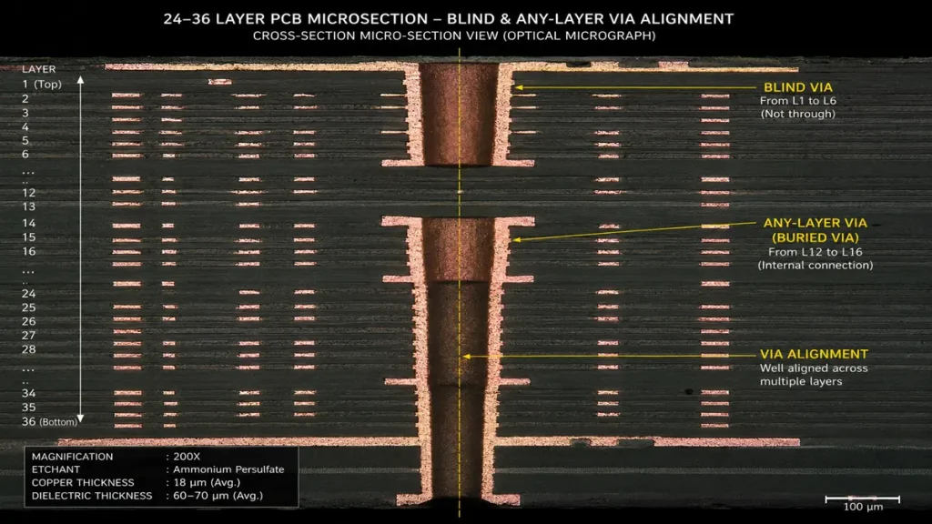
Optical micrograph (200X magnification) showing a cross-sectional micro-section view of our 36-layer Any-Layer HDI architecture. The golden centerline demonstrates high-precision via alignment across multiple layers, validating our advanced LDI registration control (≤ ±25 µm) required to eliminate impedance discontinuities in 224G PAM4 AI server designs.
- Customer Challenge: Modern GPU clusters necessitate 24-layer to 36-layer board designs utilizing advanced High-Density Interconnect (HDI) technology to route massive ball-grid array (BGA) pinouts from high-bandwidth Tensor Core processors. However, for 224G PAM4 transmission channels, deep-stack Any-layer HDI presents structural signal integrity risks due to layer misalignment and microvia impedance discontinuities.
- Our Engineering Solution: We typically recommend a hybrid architecture that restricts HDI processing to localized BGA breakout zones. This allows high-speed differential pairs to route through the precise internal stripline layers of a high-precision backplane or system board, bypassing the impedance risks of deep-stack microvias.
- Manufacturing Capability Proof: Our facilities utilize advanced Laser Direct Imaging (LDI) with automated optical alignment systems designed to control layer-to-layer registration within ≤ ±25 µm. To mitigate inner-layer separation, laser microvias are processed with optimized aspect ratios (typically 1:0.5 to 1:0.6). Production lines are regularly audited to maintain an HDI yield rate target exceeding 98.5% on multi-layer designs.
Ultra-Low Loss Material Processing for 224G PAM4 Channels
- Customer Challenge: Transitioning to 224G PAM4 data rates drives the Nyquist frequency to 56 GHz, making dielectric absorption and conductor attenuation the primary bottlenecks of signal transmission. Utilizing standard materials results in catastrophic insertion losses over typical server routing lengths.
- Our Engineering Solution: We regularly process hyper-low-loss, thermoset hydrocarbon and PTFE-infused laminates engineered specifically for high-frequency applications. These materials maintain a highly stable Dielectric Constant (D_k) and ultra-low Dissipation Factor (D_f) across wide temperature variations.
- Manufacturing Capability Proof: We maintain strategic volume partnerships and verified processing profiles for industry-standard laminates, including Panasonic Megtron 7 (R-5785 / R-5785V), Isola I-Speed, and Doosan DS-7409DV. Our etching lines are optimized for Hyper Very Low Profile (HVLP) copper foils with an average surface roughness (R_z) below 1.0 µm, minimizing skin-effect losses while achieving a copper-to-resin peel strength validated under IPC-4101E standards.
Strict Impedance Control and Complex Stack-Up Design
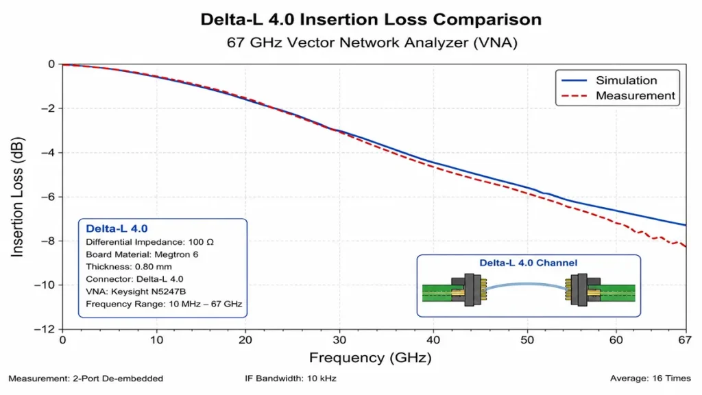
Delta-L 4.0 insertion loss comparison curves swept up to 67 GHz using a Keysight N5247B Vector Network Analyzer (VNA). The tight correlation between the blue simulation line and red measurement line demonstrates our advanced fabrication precision and capability to physically validate signal attenuation boundaries for next-generation 224G PAM4 channels.
- Customer Challenge: To eliminate high-frequency signal reflections across the backplane and accelerator board interfaces, high-speed differential pairs (such as PCIe Gen6 or NVLink interfaces) are typically specified at 85 Ω or 90 Ω ±5%. In critical high-speed channels, engineering teams often require tightening impedance deviations to ±3% to maximize transmission margins. When engineering 30+ layer server backplanes, theoretical stack-up calculations frequently fail in production due to resin starvation around heavy inner-layer copper planes.
- Our Engineering Solution: Our engineering team utilizes advanced impedance simulation software integrated with historical manufacturing material compression data. We design complex hybrid prepreg layouts—interleaving thin, high-resin glass styles (such as 106 or 1080) with thicker, structurally stable styles (such as 2116)—to support full encapsulation without trace distortion.
- Manufacturing Capability Proof: Real-time Time-Domain Reflectometry (TDR) test coupons are integrated onto production panels. Final validation is carried out via Delta-L 4.0 testing methodologies using automated 67 GHz Vector Network Analyzers (VNAs) to verify that raw board performance aligns with your SI simulation profiles.
High Current Carrying Capacity and Low PDN Impedance
- Customer Challenge: High-performance AI processors can draw up to 700W to 1000W+, pulling continuous currents exceeding 1000A at core voltages below 1V. This demands an ultra-low Power Distribution Network (PDN) target impedance—frequently sub-0.5 mΩ up to several MHz—to prevent severe voltage drop (IR Drop) and localized thermal hotspots.
- Our Engineering Solution: We fabricate stack-ups combining multi-layer heavy copper cores (2 oz to 3 oz inner layers) coupled with dense, interlocking power and ground plane structures. This maximizes cross-sectional copper volume for high-current conduction while optimizing space for adjacent high-speed signal routing layers.
- Manufacturing Capability Proof: Our automated vacuum-assisted etching lines control heavy-copper trace geometries precisely, reducing trace undercut and keeping outer/inner copper thickness tolerances within ±5%. Copper plating in via barrels is managed through periodic cross-sectional micro-section analysis to ensure a minimum continuous wall thickness of 1 mil (25 µm), fully conforming to IPC Class 3 standards.
How do Multi-GPU Interconnect, Power, and Cooling Challenges Impact Fabrication?
The Core Challenge: Manufacturing multi-GPU system boards requires resolving dense interconnect topologies, managing severe multi-layered thermal expansion, routing heavy-current Voltage Regulator Module (VRM) lines, and eliminating structural board warping caused by massive heatsink and silicon component loading.
High-Speed Interconnect Topologies and Fiber-Weave Mitigation
- Customer Challenge: At 56 GHz and above, any architectural variation in the underlying fiberglass structure can induce the fiber-weave effect. If one leg of a differential pair runs over a glass bundle while the other runs over a resin-rich gap, the difference in D_k introduces intra-pair skew, which can degrade the PAM4 eye diagram and cause bit errors in high-speed GPU-to-GPU communication links.
- Our Engineering Solution: We implement a multi-tiered mitigation strategy. First, we advise and utilize mechanically spread glass fabrics that offer a highly uniform dielectric distribution. Second, we complement this by applying a micro-angled routing matrix (typically 2 to 5 degrees) or slightly rotating the artwork during panelization to ensure traces never run perfectly parallel to the glass yarns.
- Manufacturing Capability Proof: To mitigate high-frequency resonance stubs, our facilities utilize dual-head automated controlled-depth backdrilling. We consistently achieve a target residual stub length of less than 2 mils (50 µm) across 30+ layer boards, verified by automated X-ray inspection (AXI) and optical depth-measurement systems.
Parallel Power Supply and VIPPO Processing
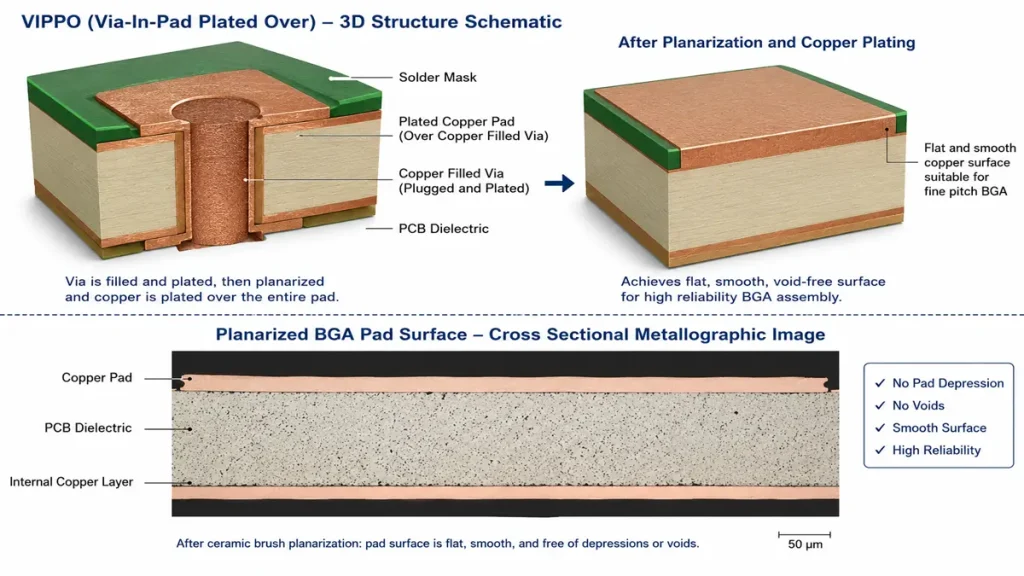
3D structure evolution and corresponding cross-sectional metallographic micrograph of our Via In Pad Plated Over (VIPPO) process flow. Following precision ceramic brush planarization, the BGA landing pad exhibits a perfectly coplanar surface (≤ ±2 mils) with zero pad depression or internal outgassing voids, effectively eliminating solder ball bridging defects during high-temperature SMT reflow.
- Customer Challenge: Delivering high current from VRMs to a multi-GPU cluster requires dense via arrays with robust copper plating within the barrels. When mechanically drilling through alternating layers of 3 oz copper power planes and ultra-thin signal layers, drill bits experience rapid wear, causing inner-layer smear and copper burrs that can lead to latent open or short circuits under thermal stress. Furthermore, vias must often be embedded directly within component landing pads to save routing space.
- Our Engineering Solution: We implement specialized drill-bit replacement protocols based on real-time hit counts and utilize advanced multi-stage chemical processing. For pad embedded routing, we execute a full Via In Pad Plated Over (VIPPO) process flow.
- Manufacturing Capability Proof: Our VIPPO process utilizes automated horizontal plugging machines to fill all staggered, blind, or buried vias with flat-curing conductive or non-conductive epoxy paste. The boards are processed through precision ceramic grinding equipment to achieve flat mounting surfaces with zero bubble entrapment, preventing assembly defects in large, fine-pitch BGA packages. Interconnect integrity is verified using advanced plasma desmear cycles paired with chemical permanganate processing.
Integrated Thermal Management Strategies
- Customer Challenge: High-density AI servers require robust hybrid cooling interfaces integrated directly into the PCB structure to prevent thermal throttling of high-value silicon components.
- Our Engineering Solution: We offer three distinct embedded thermal management configurations tailored to your enclosure and cooling architecture:
- Embedded Copper Blocks (Coin Bonding): Solid copper coins are embedded into CNC-routed cavities within the internal layers prior to lamination, providing a direct thermal path.
- High-Density Thermal Vias: Dense arrays of 10-mil thermal vias filled with high-thermal-conductivity epoxy (K = 3.5 W/(m·K)) to transfer heat from localized VRMs directly to secondary cooling planes.
- Liquid Cooling Cold Plate Interfaces: Providing precise Z-axis routing tolerances on contact zones to ensure perfectly flush seating with liquid-cooled copper cold plates.
- Manufacturing Capability Proof: Our precision CNC routing and lamination press configurations allow us to control resin flow around embedded copper coins, maintaining a flush surface coplanarity tolerance within ±2 mils (±50 µm) to guarantee structural uniformity.
Board-Level Mechanical Stability and Warpage Control
- Customer Challenge: Because an assembled GPU system board features multiple ultra-large-die BGAs, massive heatsinks, and a thick form factor, it is highly susceptible to thermal-stress warping during SMT reflow soldering. This warping is driven by Coefficient of Thermal Expansion (CTE) mismatches between the high-frequency laminates, copper planes, and fiberglass substrates.
- Our Engineering Solution: Our engineering team enforces strict symmetry across the central axis of the stack-up—matching copper density, layer distribution, and prepreg styles. We exclusively utilize high-Tg (glass transition temperature > 180 °C), low-CTE materials to provide structural stability.
- Manufacturing Capability Proof: We subject large-form-factor boards (up to 600 mm x 500 mm) to dynamic warpage testing under IPC-TM-650 standards. Our production optimization targets a board flatness deviation below 0.5% during thermal shock, ensuring reliable multi-BGA assembly alignment.
Technical Capabilities Matrix
The following matrix outlines the advanced tier fabrication thresholds our facilities maintain to support next-generation GPU ecosystems, compared against standard industry baselines:
| Technical Metric / Process Requirement | Standard Industry Baseline Capability | Our Advanced Tier Manufacturing Threshold |
|---|---|---|
| Layer Count Capability | 12 to 16 Layers | 24 to 36+ Layers (High-aspect ratio backplanes) |
| HDI Architecture Style | 1-N-1 or 2-N-2 Stackups | Any-Layer / ELIC (Every Layer Interconnect) |
| Impedance Tolerance Control | ±10% Tolerance | ≤ ±5% Strict Control (±3% for specialized channels) |
| Laser Via Aspect Ratio | 1:0.4 Maximum Depth-to-Width | 1:0.5 to 1:0.6 Precision Filling |
| Inner Copper Thickness Tolerance | ±15% Variation | ≤ ±5% on Heavy Inner Cores (Up to 3 oz) |
| High-Speed Signal Verification | Basic TDR Coupon Testing | 67 GHz VNA + Advanced Delta-L 4.0 Test Methodology |
| Surface Coplanarity (Warpage) | ≤ 0.75% over standard board sizes | ≤ 0.5% Dynamic Warpage (600 mm x 500 mm System Board) |
Real-World Case Studies & Manufacturing Provenance
Case Study 1: 32-Layer 224G PAM4 AI Architecture Backplane
An enterprise data center customer required a 32-layer ultra-high-speed backplane to support multi-chassis OAI (Open Accelerator Infrastructure) topologies. The design integrated 90 Ω differential pairs operating at Nyquist frequencies of 56 GHz. By employing Panasonic Megtron 7 (R-5785V) laminates paired with HVLP2 copper foil, our engineering team controlled the etching factor to achieve a strict ±3% impedance tolerance. To mitigate high-frequency resonances, dual-head controlled-depth backdrilling was implemented, leaving a target stub length under 35 µm. Final verification via Delta-L 4.0 testing confirmed that insertion loss remained within the specified -22 dB budget, facilitating a seamless transition from prototype to volume manufacturing.
Case Study 2: High-Power GPU Baseboard with Integrated 3 oz Heavy Copper PDN
A leading AI hardware provider faced localized thermal hotspots and severe IR drop on an 8-GPU accelerator baseboard handling peak currents up to 1200A. The structural challenge involved interleaving 4 internal layers of 3 oz heavy copper power planes with ultra-thin high-speed routing layers without causing resin starvation. Our DFM team designed a hybrid prepreg layout using high-resin 1080 styles directly against the heavy copper boundaries. Surface flatness was maintained across the large-form-factor board (580 mm x 490 mm) using strict symmetry optimization, keeping dynamic reflow warpage below 0.45%. This enabled successful zero-defect placement for 0.8 mm pitch fine-line BGAs during SMT assembly.
Real-World Technical Application Profiles
NVIDIA HGX/OAM Style AI Training Servers
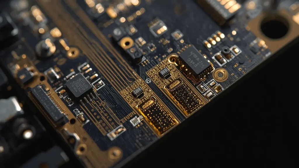
Top-down macro view of a high-density, multi-layer GPU accelerator system board, showcasing ultra-fine line trace geometries, gold-plated routing matrices, and high-pitch component placements engineered for next-generation AI training clusters.
These platforms represent the pinnacle of high-bandwidth demand, utilizing dense GPU clusters that require continuous high-frequency transmission lines. Our manufacturing priority for these applications centers on minimizing insertion loss over extended trace lengths while dissipating extreme thermal heat fluxes from tightly clustered accelerator boards. We regularly process these boards with low-loss Megtron 7 laminates and integrated copper coins to support continuous operational uptime under full computational loads.
High-Density AI Inference Platforms
Unlike training environments, inference hardware frequently targets energy efficiency and high throughput density at lower overall power thresholds. The manufacturing focus shifts toward multi-channel routing optimization, tight component spacing, and minimizing layout footprints. We can support these designs by utilizing fine-line Any-Layer HDI architectures that maintain signal integrity across edge-compute node enclosures.
Ruggedized Accelerated Computing Environments
This covers critical environments including autonomous driving computer systems, medical imaging hardware, and industrial computing clusters. The primary PCB requirement shifts to long-term environmental reliability, demanding extreme thermal shock endurance, mechanical vibration resistance, and rigorous electrochemical migration (ECM) protection across dense board layers. We meet these requirements by manufacturing fully compliant IPC Class 3 boards tested thoroughly under IST (Interconnect Stress Testing) conditions.—ons.
Frequently Asked Questions (FAQ)
Our simulations require an insertion loss budget of ≤ -25dB at 56 GHz for a 224G PAM4 channel. How does your facility physically validate this during production?
We do not rely solely on basic TDR coupon testing for ultra-high-speed channels. We embed specialized Delta-L 4.0 test coupons on every production panel and utilize an automated 67 GHz Vector Network Analyzer (VNA) to measure raw insertion loss and return loss directly. This allows us to deliver physical, data-backed evidence that your manufactured boards align with your pre-layout signal integrity simulation profiles before shipment.
High layer counts mixed with heavy copper layers often lead to resin starvation and delamination during reflow. How does your engineering team mitigate this?
During our initial DFM engineering review, we analyze the copper density of your power and ground planes. Instead of applying a uniform prepreg layer, we design a custom hybrid prepreg stack-up, pairing high-resin styles (like 106 or 1080) against the heavy copper faces to ensure complete resin filling, while using low-resin, structurally stable glass styles internally. This process, combined with our vacuum-assisted lamination presses, effectively eliminates internal micro-voids and supports delamination-free performance through multiple lead-free reflow cycles.
We use ultra-large BGAs with 0.8mm pitch for next-gen GPU accelerators. Can your VIPPO process guarantee zero outgassing or dimpling defects during SMT assembly?
Yes. Our VIPPO line utilizes flat-target ceramic planarization grinding after epoxy plugging. This achieves a surface coplanarity across the BGA landing pads of ≤ ±2 mils, eliminating the dimpling or pad protrusion that can lead to solder bridging or open joints. Furthermore, our multi-stage baking profile ensures complete curing of the plugging paste, preventing latent outgassing during your lead-free SMT reflow stages.
How does your facility support hardware procurement and engineering teams during the initial NPI (New Product Introduction) prototypes phase?
We provide an end-to-end NPI engineering service. Our dedicated signal integrity and DFM engineers collaborate directly with your layout team to cross-verify material callouts, recommend cost-effective stack-up alternatives (such as equivalent high-performance laminates), and run full design rule checks on your drill-to-copper clearances. This upfront engineering optimization accelerates your time-to-market by ensuring that your prototypes are built with a smooth path toward high-yield mass production.
Accelerate Your AI Hardware Deployment: Technical DFM & Engagement
Transitioning a high-layer-count, 224G PAM4 GPU architecture from design simulation to high-yield physical production requires rigorous upfront engineering alignment. We provide comprehensive technical support to hardware engineering teams and procurement managers during the initial NPI (New Product Introduction) and prototype phases.
Our Collaborative Engineering Framework Includes:
- Stack-up Optimization & Stack-up DFM Review: Cross-verification of material callouts (e.g., Megtron 7, Isola, Doosan) to provide identical-performance, cost-effective laminate recommendations and verify drill-to-copper clearances.
- Impedance & SI Pre-Calculation: Co-engineering trace geometry adjustments based on historical resin-compression factors to match target impedances within ±3% to ±5%.
- Thermal Management Layout Support: Feasibility analysis for embedded copper coins, high-conductivity thermal via matrices (K = 3.5 W/(m·K)), and cold-plate physical interfaces.
Data Submission Requirements for Engineering Feasibility Reviews:
To initiate a comprehensive technical assessment, stack-up validation, or automated quote, please provide the following documentation to our engineering desk:
- Gerber or ODB++ Datasets: Complete fabrication artwork, including drill files and trace layouts.
- Comprehensive IPC-2581 or Readme Specifications: Defining layer stack-up definitions, copper weights, target materials (D_k / D_f), and strict impedance parameters.
- Manufacturing Notes: Explicit callouts regarding IPC Class tolerances (Class 2 vs. Class 3), surface finish preferences (ENIG, ENEPIG), and VIPPO/backdrilling requirements.
Ready to validate your next-generation AI server architecture? Contact our technical engineering group today to schedule a formal design rule review or submit your data files for an NPI evaluation.
About Author
David Chen https://www.linkedin.com/in/pcbcoming
David Chen boasts an extensive professional background in PCBA manufacturing, PCBA testing, and PCBA optimization, with specialized expertise in high-precision PCBA fault analysis and rigorous PCBA reliability testing. The author has worked with high-layer-count server PCB fabrication, ultra-low-loss backplane stackups, and thermo-mechanical reliability optimization for AI infrastructure projects involving 112G and 224G PAM4 architectures. Skilled in complex circuit design and cutting-edge advanced PCB manufacturing processes, he delivers solutions that elevate product durability and performance across industrial applications. His technical articles focusing on PCBA manufacturing workflows and testing methodologies are widely cited by industry peers, research institutions, and technical platforms, solidifying his reputation as a recognized technical authority in the global circuit board manufacturing sector.