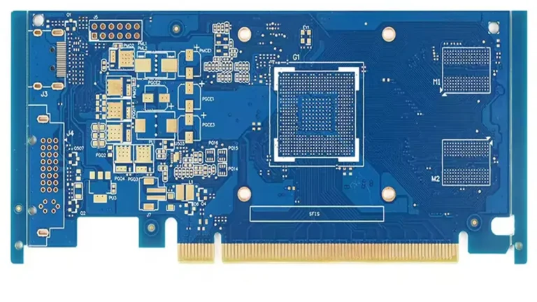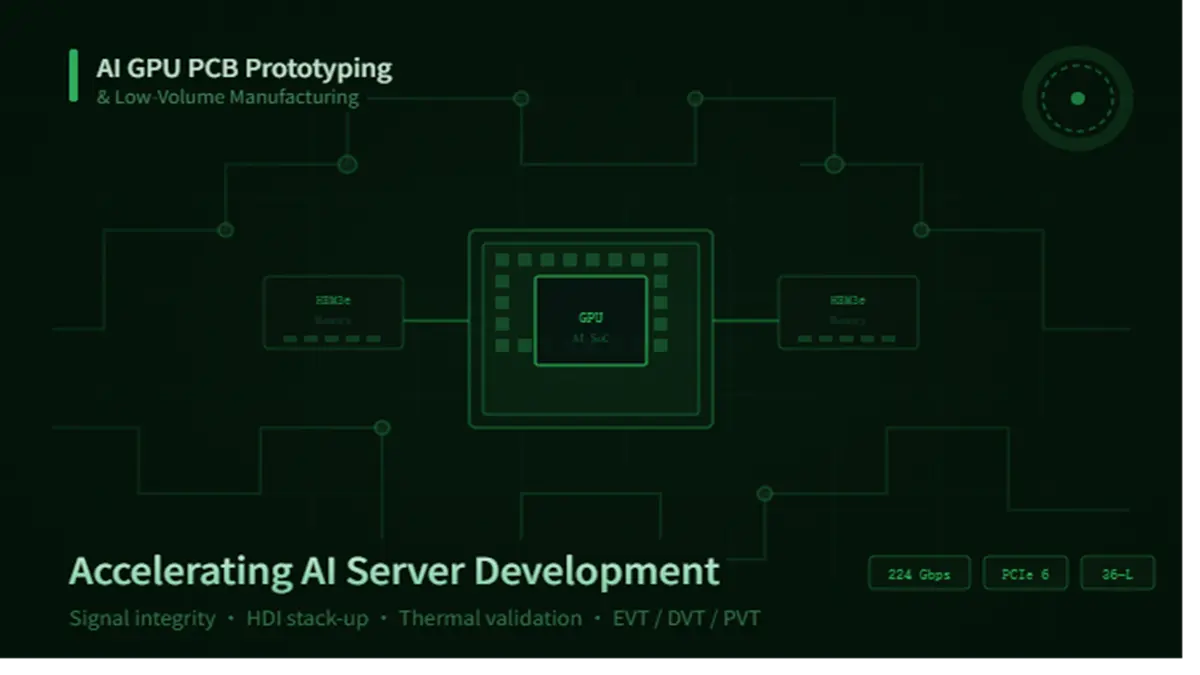
How Do AI GPU PCB Prototype and Low-Volume PCB Manufacturing Accelerate AI Server Development?
AI GPU PCB prototyping and low-volume manufacturing streamline next-generation hardware architecture development by compressing the design-to-validation cycle. This process allows engineering teams to systematically verify signal integrity, manage thermal dissipation boundaries, and evaluate high-density interconnect (HDI) routing structures under real-world operating margins.
Why Is Rapid Prototyping Critical for High-Layer AI GPU PCBs?
Rapid prototyping mitigates technical and financial risks by enabling hardware teams to empirically validate impedance matching, insertion loss, and substrate material behavior before transitioning to volume production lines.
Modern AI server hardware utilizing OAM (Open Accelerator Module) architectures or high-density PCIe accelerators requires complex electrical layouts. Engineers face condensed development schedules while managing multi-layer stack-ups that frequently range from 28 to 36+ layers. Unresolved design errors caught late in the engineering verification cycle can result in significant schedule slippage and compromised time-to-market windows.
Substrate material metrics are primary considerations during the prototype fabrication phase. Standard FR-4 materials typically demonstrate insufficient electrical and thermal performance margins for these high-frequency applications. Fabricators rely on Ultra-Low Loss (ULL) and Super Ultra-Low Loss (SULL) thermoset resin systems (such as Panasonic Megtron 7/8 or Isola Tachyon 100G) to preserve signal transitions up to 224 Gbps PAM4, ensuring compliance with PCIe Gen5/6 and High Bandwidth Memory (HBM3e/HBM4) routing parameters.
Table 1: Substrate Material Performance Metrics (Vetted via IPC-TM-650 Standards)
| Material Property (Tested per IPC-TM-650) | Standard High-Tg FR-4 (IT-180A Class) | Advanced AI GPU Substrate (e.g., Megtron 8 / Grade EA) | Metrology / Verification Method |
|---|---|---|---|
| Dielectric Constant (Dk) at 28 GHz | 4.1 – 4.4 | 2.8 – 3.0 | Split-Post Dielectric Resonator (SPDR) |
| Dissipation Factor (Df) at 28 GHz | 0.016 – 0.020 | 0.0010 – 0.0015 | IPC-TM-650 2.5.5.13 (SPDR Boundary) |
| Glass Transition Temp (Tg) | 170°C | ≥ 200°C | Thermal Mechanical Analysis (TMA) |
| Z-Axis CTE (Alpha 1 / Alpha 2) | 45 / 230 ppm/°C | 22 / 180 ppm/°C | IPC-TM-650 2.4.24 (TMA Curve) |
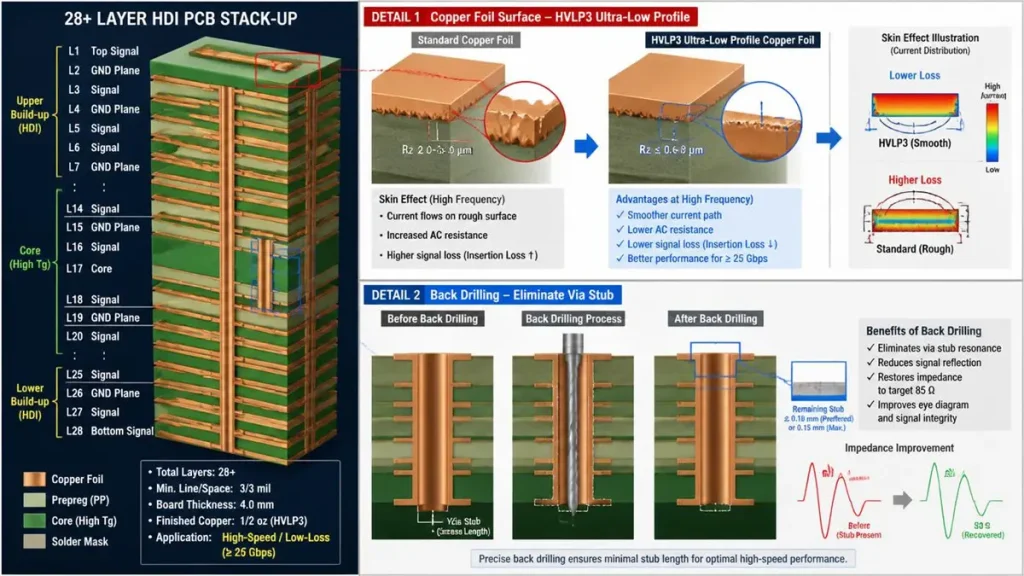
28+ Layer HDI PCB Stack-Up and Back-Drilling Signal Integrity Optimization
“At 224 Gbps data rates, skin effect losses increase significantly due to copper surface topology. For high-frequency AI GPU prototypes, we implement HVLP3 (Hyper-Very-Low-Profile) copper foils with a controlled Rz roughness under 0.6 μm. Maintaining strict copper profile boundaries during initial prototyping, verified via cross-sectional scanning electron microscopy (SEM), is necessary to prevent premature eye closure during hardware validation.”
— Signal Integrity Engineer, Shenzhen Hongda Circuit Technology Co., Ltd.
Engineering Diagnostic Report (Case Reference: SI-2026-GPU): During an evaluation of an ultra-high-speed processing board, initial Vector Network Analyzer (VNA, Keysight E5080B) testing indicated unexpected Return Loss (RL) degradation exceeding -10dB above 14 GHz. A Time-Domain Reflectometry (TDR) analysis identified a localized impedance drop down to 78Ω (against an 85Ω differential target) caused by an uncompensated via stub. Cross-sectional metrology confirmed that the controlled-depth back-drilling configuration had left a stub residue exceeding 0.15 mm due to dynamic Z-axis drill-tip wear tolerances. Adjusting the drill calibration profiles on a Schmoll laser-drilling system during the rapid prototype phase restored the differential impedance to within ±5% and avoided an expensive redesign loop during later manufacturing stages.
Engineering Tool 1: AI GPU PCB High-Layer Stack-Up & SI Validation Checklist
- Substrate Verification: Confirm Dk ≤ 3.0 and Df ≤ 0.0015 at target operating frequency (SPDR verified).
- Copper Foil Profile: Specify HVLP3 (Rz ≤ 0.6 μm) on all 112G/224G high-speed inner layers to mitigate skin effect.
- Via Stub Budget: Enforce back-drill residual stub target ≤ 0.10 mm on critical SerDes lines; flag all stubs > 0.15 mm.
- Glass-Weave Alignment: Enforce 1067/1078 spread-glass styles or specify a 10-degree trace rotation angle to mitigate differential skew.
- Tolerances: Map high-speed differential pairs to ±5% tolerance parameters rather than standard ±10%.
How Does Low-Volume AI GPU PCB Prototype Manufacturing Validate Performance and DFM?
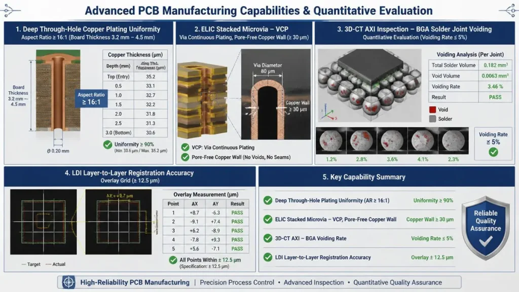
AI GPU PCB Plating Quality and Quantitative Inspection Validation
Low-volume manufacturing provides an empirically monitored environment to validate aspect ratios, microvia plating distribution, and assembly tolerances across multiple manufacturing lots, delivering statistical process capability (Cpk) data prior to high-volume scaling.
Evaluated Manufacturing Pain Points & Stress Parameters:
- Microvia Interconnect Reliability: AI GPU architectures deploy Every Layer Interconnect (ELIC) and high-density HDI stack-ups (such as 3+N+3 or 4+N+4). A key reliability focus is the structural integrity of stacked microvias during thermal cycles. Localized thermal variations occur during continuous operational loads. If the electrolytic copper plating within a 1-mil laser via contains micro-voids, the Coefficient of Thermal Expansion (CTE) mismatch between the copper barrel and the surrounding resin can lead to trace separation and intermittent signal loss. Microvia reliability is verified under IPC-TM-650 2.6.26 DC Current Induced Thermal Cycle testing.
- High-Aspect Ratio Through-Holes: With system baseboards reaching thicknesses of 3.2 mm to 4.5 mm, the aspect ratio for mechanical through-holes can exceed 16:1. Achieving uniform, continuous copper coverage within the center of these deep vertical channels is a standard manufacturing challenge.
Process Control Solutions:
To manage these parameters on the production floor, Shenzhen Hongda Circuit Technology Co., Ltd. utilizes defined manufacturing baselines during low-volume validation lots:
- Vertical Continuous Plating (VCP): Automated VCP lines and specialized organic additives are utilized to target a minimum hole-wall copper thickness of 30 μm (exceeding the IPC-6012E Class 3 target of 25 μm) across 16:1 aspect ratio profiles, reducing the risk of barrel cracking under thermal load.
- Laser Direct Imaging (LDI) Alignment: For fine-pitch BGA fields down to 0.4 mm, LDI systems maintain layer-to-layer registration within ±12.5 μm, which secures alignment margins and helps mitigate Conductive Anodic Filament (CAF) risks.
- Quantitative Assembly Inspection: The automated SMT flow incorporates 3D SPI for paste volume analysis and 3D AOI for component alignment. For high-mass components like BGAs and multi-phase VRMs, 5-axis 3D AXI (Omron 3D-CT system) is used to evaluate solder joint voiding. Engineering criteria limit internal voiding to under 5%, establishing an operational margin well within standard IPC Class 3 limits.
Engineering Tool 2: Low-Volume Pre-Production Trial Run Passing Criteria
| Inspection Category | Vetted Metric Baseline | Minimum Passing Threshold | Testing Equipment / Standard |
|---|---|---|---|
| Hole-Wall Plating Thickness | Nominal: 30 μm – 35 μm | Minimum: ≥ 28 μm | Micro-sectioning / IPC-6012E Class 3A |
| Layer-to-Layer Registration | Target: ±10 μm | Maximum Deviation: ±12.5 μm | X-Ray Metrology / LDI Real-time Log |
| BGA Solder Joint Voiding Rate | Target: ≤ 3% | Maximum Deviation: ≤ 5% | 5-Axis 3D-CT AXI / IPC-A-610 Class 3 |
| Impedance Deviation (High-Speed) | Target: 85Ω / 100Ω ±5% | Maximum Deviation: ≤ ±7% | Time-Domain Reflectometer (TDR) / Tektronix |
| Interlayer Delamination Risk | No separation after thermal shock | 6x Reflow Cycles @ 260°C | IPC-TM-650 2.6.8 Thermal Stress Test |
Common Issues in EVT, DVT, and PVT Stages for AI Hardware
Systematic hardware validation (EVT, DVT, PVT) tracks and eliminates distinct engineering anomalies ranging from layout-level crosstalk to manufacturing yield variations.
Advancing an AI processor platform from design to release involves verifying critical parameters across three distinct hardware testing phases:
- EVT (Engineering Validation Test): The primary focus during EVT is verifying fundamental Signal and Power Integrity (SI/PI). Common issues identified include trace crosstalk due to routing density, loop inductance anomalies, and voltage drops across high-current core power rails under transient load changes.
- DVT (Design Validation Test): DVT focuses on environmental, thermal, and compliance metrics. Typical challenges include EMI emission peaks exceeding regulatory limits and localized thermal hot spots. These thermal conditions test the mechanical reliability of structural materials and sub-components over extended operation.
- PVT (Production Validation Test): PVT evaluates process capability indices (Cpk) and manufacturing yield stability. Typical issues identified include panel warpage during automated reflow and lot-to-lot impedance variance. These risks are heightened if the manufacturing process window was not established during previous low-volume production runs.
The Strategic Bridge: Transitioning from AI GPU PCB Prototype to Mass Production
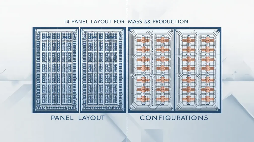
AI GPU PCB Panel Layout vs Copper Thieving Configurations
Low-volume production provides the statistical baseline required to freeze design files, verify DFM guidelines, and establish predictable yield trends prior to scaling manufacturing output.
Transitioning a high-layer-count AI PCB layout to mass manufacturing requires careful verification of process margins. Direct transitions can introduce yield risks due to subtle tool scaling behaviors, material shrinkage variations, and lamination press pressures. A structured low-volume run acts as an engineering control phase to standardize parameters and lock the final bill of materials (BOM). This methodology helps limit the risks of unexpected performance variations to within standard statistical boundaries, significantly reducing the probability of unplanned tooling modifications.
Yield Optimization Case Study (Report ID: YR-2026-92): In a multi-layer server board manufacturing run at our B2B facility, initial panels exhibited panel deformation and minor registration shifts during sequential lamination cycles, restricting initial target yields. By executing a controlled low-volume trial lot, engineering teams isolated the press pressure distribution and thermal rate-of-rise parameters. The panel layout was modified to incorporate balanced copper-thieving configurations, and the lamination cycle times were adjusted.
This process adjustment stabilized panel registration margins prior to final tooling release, contributing to a **15% yield improvement** relative to initial base manufacturing configurations and securing a stable Cpk ≥ 1.33 across subsequent mass production lots.
Engineering Tool 3: Thermal & Mechanical Co-Design Risk Metrics
| Failure Mode | Root Engineering Cause | Low-Volume Mitigation Strategy | Validation Standard |
|---|---|---|---|
| Via Barrel Shear | Z-axis CTE mismatch between resin and copper plating channel. | Deploy resin materials with Z-CTE ≤ 24 ppm/°C; enforce VCP plating min 30 μm. | IPC-TM-650 2.6.26 |
| BGA Interconnect Fatigue | X/Y warpage during reflow cycle due to asymmetric copper balance. | Enforce ≥ 45% copper balance parity across symmetric layers; implement custom aluminum reflow fixtures. | JEITA ED-4702B (Warpage ≤ 0.5%) |
| Conductive Anodic Filamentation | Resin-glass interface micro-separation under high bias voltage. | Implement laser direct imaging (LDI) alignment ≤ ±12.5 μm to isolate drilling margins. | IPC-TM-650 2.6.25 (500V DC Bias) |
Conclusion: Reducing Risk in AI GPU PCB Development
As AI infrastructure requires high routing densities and tight data transition margins, hardware design windows have narrowed. Managing these parameters across large GPU clusters requires structured manufacturing workflows. Utilizing coordinated rapid prototyping and low-volume manufacturing lots provides hardware developers with a systematic methodology to evaluate design margins. This process ensures that signal anomalies, thermal performance limits, and assembly variations are resolved, establishing a predictable path toward product introduction.
Frequently Asked Questions (FAQ)
What is the typical turnaround time for an AI GPU PCB prototype?
For complex layouts ranging from 24 to 36 layers with advanced ULL materials, standard prototype fabrication cycles typically require 7 to 10 working days following final CAM data verification, depending on HDI configuration complexity.
Why is IPC Class 3 compliance standard for low-volume AI server manufacturing?
AI servers are deployed in continuous, high-utilization environments. IPC Class 3 parameters require strict tolerances for hole-wall copper plating, inner-layer alignment, and ionic cleanliness to support system reliability under long-term thermal conditions. Adopting tighter tolerance specifications such as IPC-6012E Class 3A can extend the Mean Time Between Failures (MTBF) of modules.
How is panel warpage controlled in thick AI PCBs during assembly reflow?
Process controls include designing symmetrical layer stack-ups and utilizing rigid carrier fixtures during the reflow process. These steps maintain board coplanarity within defined manufacturing limits to prevent interconnect anomalies in fine-pitch array packages. Maximum warpage is strictly controlled to within 0.5% to prevent welding defects.
Which surface finish options are commonly selected for AI GPU PCB prototyping?
ENEPIG (Electroless Nickel Electroless Palladium Immersion Gold) and Immersion Silver are common selections. ENEPIG offers flat pad topography for fine-pitch component placement and maintains performance through multiple lead-free reflow cycles.
Can low-volume manufacturing parameters be transferred to high-volume production?
Yes. By utilizing consistent design rules, tooling baselines, and material specifications during the low-volume phase at Shenzhen Hongda Circuit Technology Co., Ltd., the transition to larger manufacturing lots can proceed without requiring layout modifications or redesigning signal paths.
For technical whitepaper requests, stack-up co-design reviews, or raw material boundary analysis, contact our enterprise B2B engineering facility directly via pcb@pcbkr.com.
Find Out About Us: Delivering Top-Tier Fabrication for Both AI & Conventional PCBs
Navigating the line between cutting-edge innovation and high-volume, cost-effective production shouldn’t be a compromise. At Shenzhen Hongda Circuit Technology (PCBKR), we bridge this gap by elevating the manufacturing standards for both high-performance AI hardware and traditional multi-layer PCBs.
By integrating advanced manufacturing methodologies across all production lines, we bring an elite level of precision to traditional PCB fabrication. Our standard boards benefit from enhanced interlayer alignment tolerances (down from ±75μm to within ±25μm) and tightened differential impedance control (±5%). Supported by 100% 3D X-Ray (AXI) inspection, your conventional boards achieve chip-level reliability, superb signal stability, and near-100% yield.
Your Strategic Manufacturing Partner
We proudly stand as a dual-capability partner: offering the elite technical ceiling required for next-gen AI hardware, while maintaining the exceptional flexibility, rapid turnaround, and unmatched cost-efficiency needed for mid-to-high-volume traditional board campaigns. You get zero-defect reliability without the premium overhead or bureaucracy of massive tier-1 factories.
Ready to upgrade your hardware’s reliability?
Submit your Gerber files today for an agile engineering review and a highly competitive quote.
📧 Contact our experts: sales@pcbkr.com
About Author
David Chen https://www.linkedin.com/in/pcbcoming
David Chen boasts an extensive professional background in PCBA manufacturing, PCBA testing, and PCBA optimization, with specialized expertise in high-precision PCBA fault analysis and rigorous PCBA reliability testing. The author has worked with high-layer-count server PCB fabrication, ultra-low-loss backplane stackups, and thermo-mechanical reliability optimization for AI infrastructure projects involving 112G and 224G PAM4 architectures. Skilled in complex circuit design and cutting-edge advanced PCB manufacturing processes, he delivers solutions that elevate product durability and performance across industrial applications. His technical articles focusing on PCBA manufacturing workflows and testing methodologies are widely cited by industry peers, research institutions, and technical platforms, solidifying his reputation as a recognized technical authority in the global circuit board manufacturing sector.