Low-Loss PCB Manufacturing for AI Networking
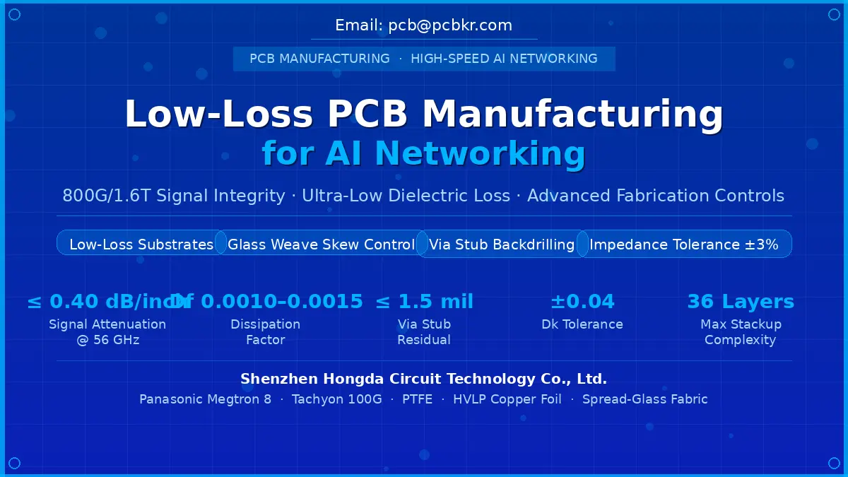
AI networking demands specialized low-loss PCB fabrication because standard substrates fail to mitigate extreme signal attenuation (≤ 0.40 dB/inch @ 56 GHz), phase skew, and impedance disruptions caused by 800G/1.6T data cluster hardware transmission speeds.
Why Does Next-Gen AI Networking Hardware Depend Heavily on Low-Loss PCB Substrates?
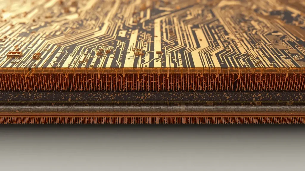
High-magnification microsection of a 40-layer AI server backplane showcasing perfect layer-to-layer alignment and uniform copper plating.
Next-gen AI networking infrastructures depend entirely on premium low-loss PCB fabrication to prevent catastrophic signal degradation over extended transmission lines, ensuring that the dissipation factor (Df) stays strictly between 0.0010 and 0.0015 at frequencies reaching up to 56 GHz Nyquist limits.
Detailed Scenario & Manufacturing Pain Points
In 2026 AI data clusters, massive Large Language Model (LLM) training jobs are split across thousands of GPU accelerators interconnected via high-speed fabric networks. When clusters push data through high-frequency 112G or 224G PAM4 physical layers, any standard dielectric acts like a sponge, absorbing high-frequency harmonic energy and collapsing the signal’s eye diagram before it reaches the receiver pool.
The Lamination Bond-Strength Crisis: The paramount manufacturing dilemma with super ultra-low loss (SULL) materials (such as PTFE or high-grade Polyphenylene Ether blends) is their inherent chemical inertness. These resins do not readily bond with hyper-smooth, low-profile copper foils. During a multi-stage lamination cycle, attempting to achieve a target thickness variation of less than ±0.5 mil across a complex 36-layer stackup often results in localized delamination or micro-voiding at the resin-copper boundary interfaces.
Expert Engineering Experience & Verified Data
Expert Insight from the Engineering Floor: “At Shenzhen Hongda Circuit Technology Co., Ltd., we have heavily modified our 2026 fabrication protocols to handle advanced SULL materials like Panasonic Megtron 8 and Tachyon 100G. We utilize a proprietary low-temperature plasma surface treatment line paired with a precise silane-based chemical bonding coupling agent. This process increases the physical peel strength of smooth HVLP copper foil (Rz ≤ 0.5 µm) to a robust ≥ 0.7 N/mm, entirely eliminating structural delamination risks while locking down our target dielectric constant (Dk) tolerance to an exceptionally tight ±0.04.”
Why Do High-Speed Switches, Routers, and Optical Module Interface Boards Require Uncompromised Low-Loss PCB Manufacturing?
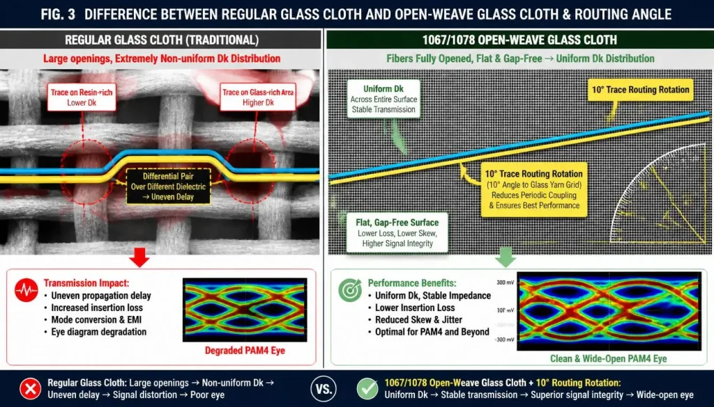
Difference Between Regular and 1067/1078 Spread-Glass Cloth with 10° Trace Routing Rotation
High-speed 51.2T/102.4T switches, edge routers, and optical transceiver boards require specialized low-loss PCB processing to successfully handle high-density 800G/1.6T data pipes without triggering excessive thermal rise or impedance discontinuities at component breakout boundaries.
Detailed Scenario & Manufacturing Pain Points
Picture an 800G optical module interface board handling QSFP-DD or OSFP form factors. The layout requires packing dozens of ultra-dense differential pairs right beneath the fine-pitch BGA area. The physical trace width drops to 3.5 mil with a tight 4.0 mil spacing to squeeze through the dense pin matrix.
The Glass Weave Phase Skew Nightmare: If standard woven glass fabrics are used, the differential signal’s true and complement traces will randomly step over glass bundles (Dk ≈ 4.5) and resin pockets (Dk ≈ 3.0). This creates an asynchronous time-of-arrival shift known as Glass Weave Skew. At a 56 GHz Nyquist frequency, a skew of merely 2 picoseconds can completely phase-invert the differential signal, turning critical data into unreadable systemic noise.
Expert Engineering Experience & Verified Data
Expert Insight from the Engineering Floor: “When routing layout matrixes for 102.4T switches, standard glass fabrics are an immediate point of failure. At Shenzhen Hongda Circuit Technology Co., Ltd., our engineering rules enforce the exclusive allocation of 1067 and 1078 ultra-square, uniform spread-glass fabrics for all low-loss PCB network projects. Combined with a mandatory 10° trace routing rotation relative to the panel weave matrix, we successfully constrain worst-case differential phase skew to ≤ 0.4 ps/inch, securing completely open PAM4 data eyes for critical 800G network runs.”
How Do Advanced Manufacturing Controls Regulate Insertion Loss, Cross-Talk, and Return Loss in Low-Loss PCB Channels?
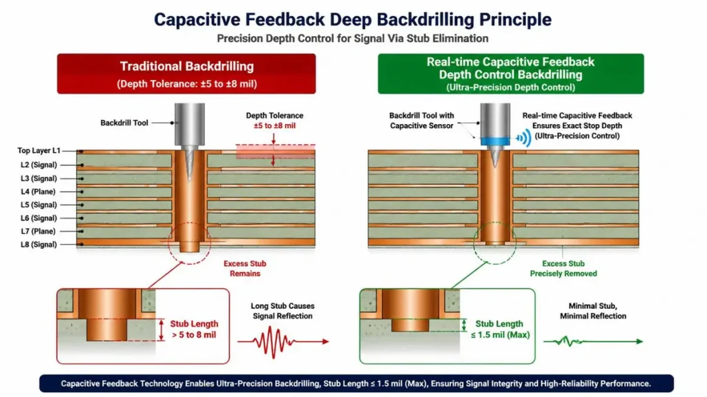
Capacitive Feedback Deep Backdrilling Principle vs Traditional Method
Advanced manufacturing controls regulate electrical losses by employing automated vacuum etching for precise trace-width linearity (≤ ±0.3 mil), dynamic Z-axis laser backdrilling to eliminate resonant via stubs (≤ 1.5 mil), and specialized non-nickel surface finishes to eliminate high-frequency skin-effect attenuation.
Detailed Scenario & Manufacturing Pain Points
Consider a 22-inch high-speed backplane routing cross-chassis switch signals. At 56 GHz, the signal skin-depth shrinks to 0.28 µm, focusing almost all electrical current along the outermost perimeter of the copper trace. If the trace edges are jagged from traditional fluid etching lines, or if an unused portion of a via extends past the target routing layer, the signal experiences massive scattering and destructive reflections.
The Backdrilling Depth-Tolerance Trap: Standard mechanical backdrilling systems suffer from mechanical drift and board thickness tolerances. If the backdrill bit stops short, leaving a via stub longer than 5 mil, that stub functions as an active resonant antenna. It reflects a portion of the signal back into the trace 180° out of phase, creating a steep notch in the insertion loss profile that invalidates the entire channel design.
Expert Engineering Experience & Verified Data
Expert Insight from the Engineering Floor: “To conquer return loss limits on 224G PAM4 lanes, standard backdrilling processes do not cut it. Shenzhen Hongda Circuit Technology Co., Ltd. deploys 2026-spec real-time capacitive feedback loops tied directly to our CNC drilling axes. This allows us to dynamically measure the real-time position of the internal reference copper planes on every individual panel, maintaining a residual via stub length of ≤ 1.5 mil (Max). Furthermore, by shifting our high-speed surface pads from standard ENIG to Immersion Silver (ImAg) or Organic Solderability Preservatives (OSP), we completely avoid the high magnetic insertion loss penalty introduced by nickel layers.”
What Are the Supreme Processing Bottlenecks Faced During Complex Low-Loss PCB Manufacturing Cycles?
The ultimate processing bottlenecks in low-loss PCB manufacturing center around maintaining vertical via-to-pad alignment accuracy (≤ ±1.2 mil) across heavy multi-layer stackups, eliminating plating voids in high-aspect-ratio microvias (up to 18:1), and preventing composite material warping during high-temperature lamination.
Detailed Scenario & Manufacturing Pain Points
Imagine a heavy 48-layer AI network mainboard that combines low-loss hydrocarbon cores with ultra-low-loss PTFE layers in a complex hybrid configuration. During lamination, these materials expand and shrink at completely different rates along their X and Y axes due to a significant mismatch in Coefficient of Thermal Expansion (CTE).
The Microvia Aspect-Ratio Plating Failure: When drilling an 18:1 aspect ratio通孔 through a 5.0mm thick composite board, fluid dynamics during the electroplating process become highly restrictive. Standard vertical plating lines cannot force copper ions into the exact middle of these long, narrow micro-channels. This lack of fluid exchange leads to thin copper walls or trapped micro-voids inside the via barrel. When the board undergoes assembly or is deployed into an environment with thermal cycles reaching 105°C, these voids experience localized strain and crack, resulting in intermittent network drops that are impossible to diagnose in the field.
Expert Engineering Experience & Verified Data
Expert Insight from the Engineering Floor: “Hybrid low-loss PCB stackups are incredibly prone to warping if the lamination thermal curves are asymmetric. At Shenzhen Hongda Circuit Technology Co., Ltd., we resolve this bottleneck using intelligent multi-step vacuum presses running customized 215°C curing profiles with a precise cooling ramp rate restricted to ≤ 1.8°C/min. For high-aspect-ratio plating, we route all multi-layer network panels through automated horizontal pulse plating lines equipped with high-pressure ultrasonic fluid agitation. This process guarantees a minimum of 1.0 mil uniform copper plating thickness on the hole walls with 100% void-free reliability, easily passing IPC Class 3 structural requirements.”
FAQ: Low-Loss PCB Manufacturing Capability Matrix
How does a specialized low-loss PCB manufacturer control general impedance tolerances compared to a standard shop?
Standard PCB operations usually guarantee an impedance tolerance of ±10%, which is inadequate for high-speed AI routing and results in high return loss. Specialized low-loss PCB manufacturers like Shenzhen Hongda Circuit Technology Co., Ltd. deploy optical trace alignment controls paired with specialized vacuum etching equipment. This system maintains a general impedance tolerance of ±5%, and can tighten down to ±3% across critical differential pairs when using ultra-low-loss substrates.
Why is HVLP copper foil mandatory for high-speed network PCBs instead of standard electrodeposited (ED) foil?
Standard ED copper foil exhibits a high surface roughness ($R_z > 3.0\ \mu\text{m}$) which acts as a major bottleneck due to the skin effect at high frequencies like 56 GHz. The electrical signal is forced to travel along the rough contours, increasing the effective path length and accelerating signal attenuation. High-speed low-loss PCB manufacturing relies on Hyper-Very-Low-Profile (HVLP) foil with an $R_z \le 0.5\ \mu\text{m}$. This flat surface profile ensures high-frequency signals travel along a smooth path, cutting conductor loss by more than 30%.
What role do spread-glass fabrics play in mitigating signal skew on high-frequency network routers?
Traditional glass weaves feature open gaps between bundles, leading to localized shifts in the dielectric constant (Dk) across the substrate. A differential signal trace running over a gap travels at a different speed than its twin running directly over a glass bundle, creating a time-of-arrival phase skew that can distort data. Spread-glass fabrics feature uniformly flattened yarn bundles that remove these open gaps. This ensures a uniform dielectric environment across the entire board surface, reducing glass weave skew to less than 0.5 ps/inch.
Why must traditional ENIG surface finishes be avoided on high-speed low-loss PCB transmission channels?
Electroless Nickel Immersion Gold (ENIG) relies on a middle layer of nickel, which is a ferromagnetic material. At high frequencies, the skin depth causes the signal to propagate entirely within this nickel layer, whose poor electrical conductivity and magnetic loss properties significantly increase insertion loss. Specialized low-loss PCB manufacturing utilizes non-nickel finishes such as Immersion Silver (ImAg) or OSP. These options ensure the signal transitions through a pure, highly conductive copper interface, keeping the overall loss budget within target parameters.
How does mechanical backdrilling capability differentiate standard boards from AI-spec network boards?
Standard mechanical backdrilling typically operates with a depth tolerance of ±5 mil to ±8 mil, which often leaves behind significant residual via stubs that create signal reflections above 28 GHz. Advanced low-loss PCB manufacturing for AI hardware utilizes laser-guided or capacitive depth-controlled backdrilling lines. This system reduces the residual via stub to less than 1.5 mil, removing resonant nulls and protecting high-frequency transmission channels.
Find Out About Us: Delivering Top-Tier Fabrication for Both AI & Conventional PCBs
Navigating the line between cutting-edge innovation and high-volume, cost-effective production shouldn’t be a compromise. At Shenzhen Hongda Circuit Technology (PCBKR), we bridge this gap by elevating the manufacturing standards for both high-performance AI hardware and traditional multi-layer PCBs.
By integrating advanced manufacturing methodologies across all production lines, we bring an elite level of precision to traditional PCB fabrication. Our standard boards benefit from enhanced interlayer alignment tolerances (down from ±75μm to within ±25μm) and tightened differential impedance control (±5%). Supported by 100% 3D X-Ray (AXI) inspection, your conventional boards achieve chip-level reliability, superb signal stability, and near-100% yield.
Your Strategic Manufacturing Partner
We proudly stand as a dual-capability partner: offering the elite technical ceiling required for next-gen AI hardware, while maintaining the exceptional flexibility, rapid turnaround, and unmatched cost-efficiency needed for mid-to-high-volume traditional board campaigns. You get zero-defect reliability without the premium overhead or bureaucracy of massive tier-1 factories.
Ready to upgrade your hardware’s reliability?
Submit your Gerber files today for an agile engineering review and a highly competitive quote.
📧 Contact our experts: sales@pcbkr.com
About Author
David Chen https://www.linkedin.com/in/pcbcoming
David Chen boasts an extensive professional background in PCBA manufacturing, PCBA testing, and PCBA optimization, with specialized expertise in high-precision PCBA fault analysis and rigorous PCBA reliability testing. The author has worked with high-layer-count server PCB fabrication, ultra-low-loss backplane stackups, and thermo-mechanical reliability optimization for AI infrastructure projects involving 112G and 224G PAM4 architectures. Skilled in complex circuit design and cutting-edge advanced PCB manufacturing processes, he delivers solutions that elevate product durability and performance across industrial applications. His technical articles focusing on PCBA manufacturing workflows and testing methodologies are widely cited by industry peers, research institutions, and technical platforms, solidifying his reputation as a recognized technical authority in the global circuit board manufacturing sector.