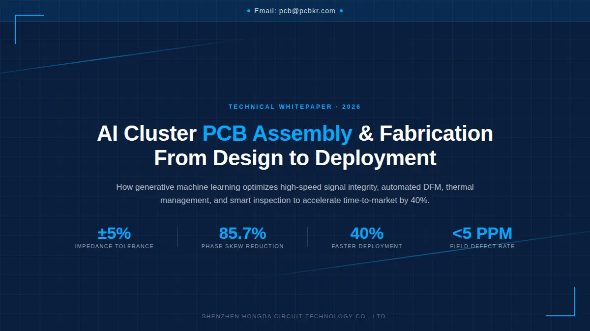
How Do AI Cluster PCB Assembly and Fabrication Services Optimize Performance from Design to Deployment?
The Architectural Ecosystem of AI Cluster Hardware
AI cluster hardware architectures depend on an interconnected, low-latency ecosystem of diverse, high-layer-count printed circuit boards. To support the massive computational density of modern training and inference clusters, the hardware infrastructure must be evaluated as a holistic system rather than isolated components. The core architecture comprises:
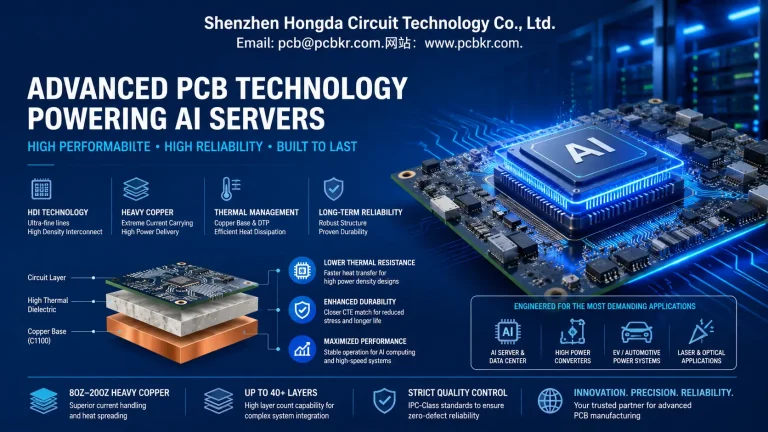
AI Server Motherboards: Designed for ultra-dense routing to interface multiple high-wattage CPUs, GPUs, and advanced memory subsystems (HBM/DDR5).
High-Speed Backplanes: Ultra-thick, high-layer-count orthogonal matrices engineered for dense interconnects and high-bandwidth, error-free data transfer between nodes.
Daughter Cards & Accelerator Modules (OAM/UBB): Specialized high-density compute expansion units requiring rigorous thermal and signal integrity control.
Power Distribution Boards: Heavy-copper, multi-layer architectures built to deliver stable, high-current, and highly efficient power delivery while minimizing IR drop.
At Shenzhen Hongda Circuit Technology Co., Ltd., we specialize in the end-to-end fabrication and assembly of this entire hardware matrix, ensuring that each board type is electrically and mechanically synchronized to prevent system-level bottlenecks.
Why Fabrication + Assembly Integration Matters for AI Infrastructure
For AI cluster hardware operating at ultra-high frequencies and massive thermal loads, treating PCB fabrication and PCBA assembly as decoupled processes is a critical risk factor. If material selection, stackup engineering, via structures, and automated surface-mount technology (SMT) reflow profiles are not co-designed, system-level signal integrity and manufacturing yields will inevitably suffer.
Integrated manufacturing ensures that design intent directly aligns with empirical shop-floor capabilities. For example, a tightening of impedance tolerances during fabrication directly affects the solder fillet reliability of fine-pitch BGAs during assembly. By bridging these two domains under a single unified engineering team, Hongda eliminates vendor handoff friction, mitigates mismatched engineering specifications, and shortens the New Product Introduction (NPI) cycle by running parallel design-for-manufacturability (DFM) check loops. For hyperscale AI deployments, this structural integration is the definitive factor in ensuring stable data transmission, eliminating costly field rework, and maximizing program velocity.
How Backplanes, Motherboards, and Daughter Cards Are Coordinated and Produced Together
Manufacturing the constituent boards of an AI cluster requires a synchronized fabrication environment. Because the backplane, motherboard, and daughter cards physically mate via high-density connectors, their mechanical registration, layer alignment, and material characteristics must be perfectly harmonized to ensure absolute system stability.
1. Ultra-High-Speed Signal Integrity & Dynamic Stackup Engineering
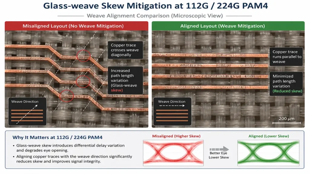
Microscopic Comparison of Glass-weave Skew Mitigation for 112G/224G PAM4 High-Speed Routing
Traditional CAM systems assume ideal, homogeneous material properties, failing to address glass-weave skew at 112G and 224G PAM4 routing speeds. At frequencies above 28 GHz, the alignment of copper traces relative to fiberglass bundles versus resin-rich pockets causes phase delays that ruin signal synchronization.
To eliminate this, Hongda’s manufacturing cluster parses incoming ODB++ design databases through an empirical data model trained on a multi-spectral substrate library (including Panasonic Megtron 8 and Tachyon 100G). The system calculates localized resin-flow profiles and substrate periodicity to enforce an optimal off-angle routing matrix—typically tracking θ = 7.5° to 11.3° layout offsets relative to the material weave.
Our cloud-assisted cluster utilizes high-fidelity deep learning surrogate models rather than slow, traditional full-wave 3D-EM solvers. By evaluating thousands of sub-via geometries per minute, the cluster predicts exact resonance notches across the 10 GHz to 70 GHz bands. This automatically determines exact microvia pad configurations and backdrilling depth parameters to ensure controlled stub lengths (Lstub ≤ 0.10 mm), capping insertion loss below -1.5dB before toolpath generation. Concurrently, our closed-loop stackup analyzer monitors copper density distribution across ultra-dense 32-layer AI backplanes, maintaining structural symmetry to keep overall board bow and twist strictly below 0.5%.
2. Advanced HDI Matrix & Automated DFM Optimization
High-Density Interconnect (HDI) structures utilizing Every Layer Interconnect (ELIC) are highly susceptible to chemical processing defects during wet etching. Micro-copper slivers (< 3 mils) frequently fracture during alkaline or acid etching, redepositing across adjacent tracks and causing micro-shorts that are invisible until final testing.
In any-layer HDI layouts featuring restricted 0.35 mm BGA pitches, manual CAM reviews take up to 48 hours and miss micro-level spacing bottlenecks. Our automated workflow addresses this through specialized geometric-inference algorithms. The system instantly identifies clearances dropping below a critical 2.5 mil threshold, dynamically performing localized, mathematically compensated teardropping at microvia junctions and optimizing outer-layer copper thieving balance. This stabilizes the chemical etch factor:
E = W / T
(Where W is the compensated trace width and T is the copper thickness).
By managing fluid boundary layers across the vertical continuous plating line, our system maintains an etch factor E ≥ 3.5, eliminating manufacturing defects in dense escape fields.
How Advanced Assembly and Validation Definitively Affect Reliability, Latency, and Yield
The final assembly and testing stages represent the ultimate validation of an AI cluster’s performance metrics. Poor solder joints, micro-voiding, or uneven thermal profiles do not just cause structural defects; they directly manifest as intermittent transmission errors, increased signal latency, packet drops, and premature field failures.
1. AI Cluster PCB Assembly and Fabrication Services Thermodynamic Optimization to Safeguard Assembly Yields
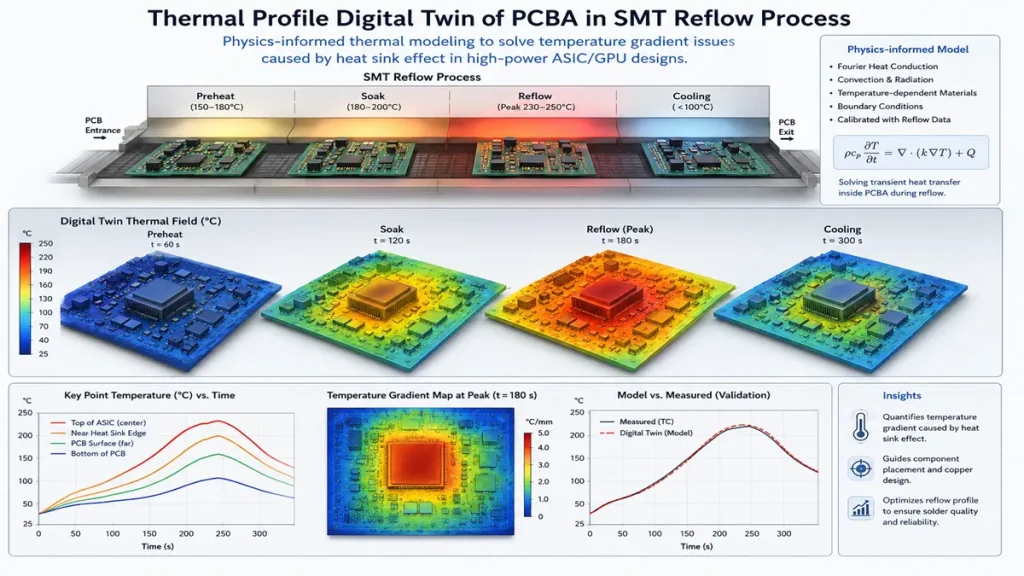
Thermal Profile Digital Twin and Thermodynamic Simulation Field of PCBA in SMT Reflow Oven
High-power AI accelerator cards and EV powertrain modules generate immense localized thermal energy. Traditional engineering relies on static, uniform thermal via grids. However, during automated SMT reflow assembly, these massive copper structures act as heat sinks, drawing thermal energy away from component pads too quickly. This results in severe thermal deltas across the PCBA, triggering cold solder joints, component tombstoning, and micro-delamination.
To secure maximum assembly yield, Hongda utilizes physics-informed thermal modeling to build a comprehensive digital twin of the PCBA prior to assembly. The system evaluates localized thermal distribution by solving a modified version of Fourier’s Law of Heat Conduction tailored for heterogeneous structures:
q = -[kij] ∇T
(Where [kij] represents the directional thermal conductivity tensor of the non-homogeneous FR4/copper matrix, and ∇T is the spatial temperature gradient).
Instead of uniform via arrays, our system designs target-staggered microvia fields and schedules precise mechanical routing paths for embedded copper coins directly beneath the high-wattage ASICs. By coupling these models with our nitrogen-purged, 10-zone reflow convection ovens, the system adjusts zone-specific convection fan frequencies and temperature ramps in real time based on the board’s exact copper distribution. This limits the peak reflow temperature delta to less than ±2.0°C across the surface of a massive 6.0 mm thick backplane, completely preventing internal delamination and thermal stress defects.
2. AI Cluster PCB Assembly and Fabrication Services Advanced Volumetric Inspection to Enforce System Reliability & Zero-Latency Signaling
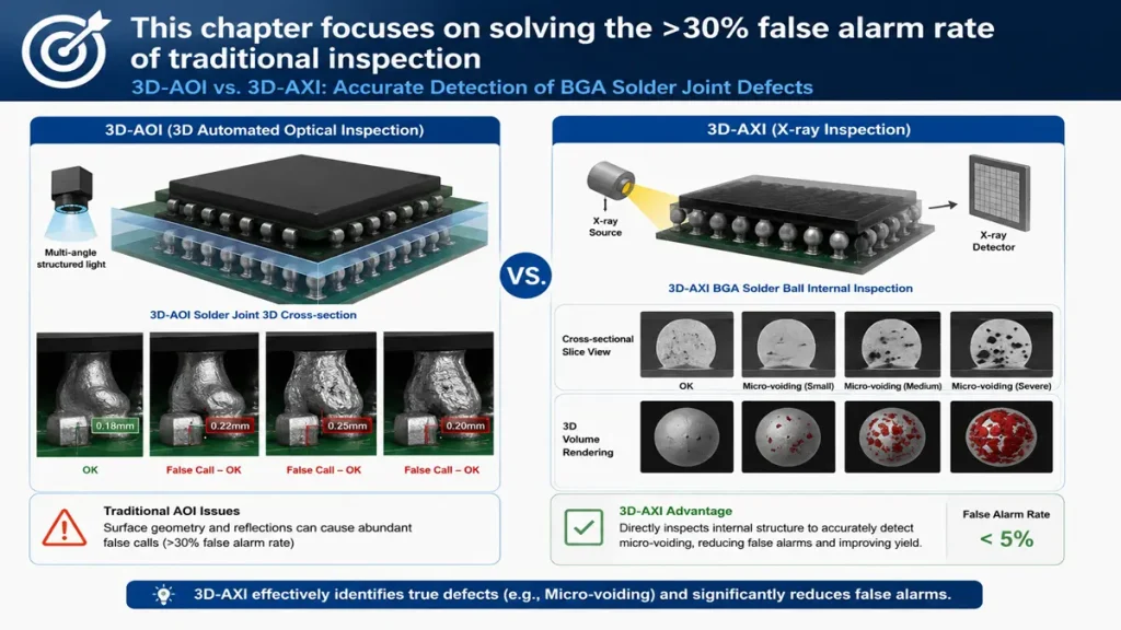
Comparative Evaluation of 3D-AOI False Calls vs. 3D-AXI Volumetric Micro-voiding Detection on Fine-Pitch BGAs
In hyperscale data centers deploying volume enterprise network switches, a single escaped defect—such as a microscopic solder crack or a “Head-in-Pillow” (HiP) BGA fault on a 1,156-pin package—will initially pass continuity checks but fail catastrophically after 90 days due to thermal expansion and vibration cycle stresses. This causes devastating field downtime and severe recall liabilities.
Shenzhen Hongda eliminates legacy, template-matching 3D-AOI false calls (which often exceed 30% due to reflective lead-free solder fillets) by integrating trained convolutional neural networks (CNNs) into the inspection line. Our 3D-AOI capture arrays measure multi-angle volumetric data of every single solder joint, analyzing the true wetting angle (θwet ≤ 30°) and solder volume distribution. For bottom-terminated components, our inline 3D-AXI system performs high-speed slice reconstruction to measure micro-voiding inside the solder spheres. If voiding exceeds exactly 10% of the total sphere area, or if the shape eccentricity deviates from structural tolerances, the AI cluster flags it for automated laser rework, driving field defect rates below 5 PPM and guaranteeing zero packet latency caused by signal discontinuities.
AI Cluster PCB Assembly and Fabrication Services, The Turnkey / One-Stop Service Model: Accelerating Deployment Time-to-Market
For global enterprises building next-generation AI infrastructure, managing a fragmented supply chain across multiple material suppliers, independent PCB fabricators, and standalone assembly houses is a primary cause of project delay.
Shenzhen Hongda Circuit Technology Co., Ltd. provides a fully centralized, Turnkey One-Stop Service Model that integrates the complete lifecycle of AI hardware development:
[ Secure DFM & Material Optimization ] ➞ [ Synchronized Multi-Board Fabrication ] ➞ [ Co-Designed SMT Assembly ] ➞ [ Advanced Volumetric Inspection & Test ]
By owning the complete workflow, we consolidate stackup optimization, controlled impedance fabrication, automated SMT assembly, precision backdrilling, and advanced 3D-AXI verification under one single engineering authority. This end-to-end model provides profound advantages:
First-Time-Right Prototyping: By aligning fabrication tolerances with assembly reflow behaviors up front, we reduce standard advanced prototyping spins to exactly 1, eliminating empirical guesswork.
40% Accelerated Deployment Schedules: Compressing the gap between independent engineering reviews allows our customers to move seamlessly from NPI to volume production without switching vendors or altering design matrices.
Guaranteed IP Protection: All proprietary layout data (ODB++ / IPC-2581) is processed through secure, localized gateways, ensuring your next-generation silicon architectures and netlist logic remain completely protected.
Partnering with Shenzhen Hongda means transitioning from fragmented manufacturing to a unified, elite engineering partnership—delivering the reliability, latency control, and yield optimizations required to power the global AI revolution.
Frequently Asked Questions (FAQ) – Comparative Evaluation
How does Hongda’s AI-assisted impedance control compare to traditional polar solvers?
Traditional design relies on static polar solvers that assume perfectly uniform substrate characteristics, yielding a wide ±10% to ±12% variance during real-world production. In contrast, Shenzhen Hongda’s manufacturing cluster analyzes actual resin-flow dynamics and empirical chemical copper-etching parameters from active line conditions. By dynamically compensating manufacturing photolithography tools, we guarantee an ultra-tight ±5% impedance stability, tightening to ±3% on critical internal signal layers.
What differentiates your automated DFM engine from standard manual CAM verification?
Standard DFM depends on static rule checklists executed by human CAM engineers over a 24 to 48-hour cycle, a method highly prone to error within dense, fine-pitch BGA escape fields where pitch is restricted to 0.35 mm. Our automated geometric-inference engine processes complete ODB++ databases in under 15 minutes, cross-referencing multi-layer configurations against real-time manufacturing capabilities to instantly resolve micro-slivers, acid traps, and localized plating bottlenecks before the files ever touch photolithography tooling.
How do your surrogate thermal models outperform legacy passive thermal management?
Legacy approaches implement uniform, unoptimized thermal via arrays based on generic component datasheets, which frequently trigger component tombstoning or cold solder joints due to uneven heat absorption during automated SMT reflow. Our physics-informed machine learning builds a highly accurate thermodynamic digital twin of the specific board geometry, solving a modified Fourier’s Law to calculate exact tensor conductivity. This optimizes the precise structural positioning of staggered microvias and custom copper coins while informing automated, real-time reflow oven profiling.
Why is CNN-driven 3D-AOI/AXI inspection superior to template-based inspection in AI environments?
Traditional template-matching systems rely on rigid pixel comparisons, generating immense false-alarm rates (>30%) due to reflective lead-free solder fillets, which causes operator fatigue and leads to true defect escapes. Our inspection lines integrate trained convolutional neural networks (CNNs) to evaluate true volumetric wetting angles (θwet ≤ 30°) and internal solder ball voiding percentages. This effectively reduces false calls to under 1% while driving the field escape rate down to a near-zero threshold (under 5 PPM), securing zero packet latency caused by signal discontinuities.
How does the deployment timeline of your Turnkey One-Stop model compare to conventional decoupled manufacturing?
Conventional decoupled workflows experience severe timeline expansion due to fragmented communication and “blame-shifting” between independent board fabricators and SMT assembly vendors, alongside high prototype failure rates (averaging 3–5 spins for advanced high-frequency boards). By aligning material selection, trace-weave compensation, and reflow thermal modeling into a single, automated pre-production workflow, Shenzhen Hongda compresses the engineering validation phase. This reduces advanced prototyping spins to exactly 1, accelerating the overall time-to-market deployment by 40%.
Find Out About Us: Delivering Top-Tier Fabrication for Both AI & Conventional PCBs
Navigating the line between cutting-edge innovation and high-volume, cost-effective production shouldn’t be a compromise. At Shenzhen Hongda Circuit Technology (PCBKR), we bridge this gap by elevating the manufacturing standards for both high-performance AI hardware and traditional multi-layer PCBs.
By integrating advanced manufacturing methodologies across all production lines, we bring an elite level of precision to traditional PCB fabrication. Our standard boards benefit from enhanced interlayer alignment tolerances (down from ±75μm to within ±25μm) and tightened differential impedance control (±5%). Supported by 100% 3D X-Ray (AXI) inspection, your conventional boards achieve chip-level reliability, superb signal stability, and near-100% yield.
Your Strategic Manufacturing Partner
We proudly stand as a dual-capability partner: offering the elite technical ceiling required for next-gen AI hardware, while maintaining the exceptional flexibility, rapid turnaround, and unmatched cost-efficiency needed for mid-to-high-volume traditional board campaigns. You get zero-defect reliability without the premium overhead or bureaucracy of massive tier-1 factories.
Ready to upgrade your hardware’s reliability?
Submit your Gerber files today for an agile engineering review and a highly competitive quote.
📧 Contact our experts: sales@pcbkr.com
About Author
David Chen https://www.linkedin.com/in/pcbcoming
David Chen boasts an extensive professional background in PCBA manufacturing, PCBA testing, and PCBA optimization, with specialized expertise in high-precision PCBA fault analysis and rigorous PCBA reliability testing. The author has worked with high-layer-count server PCB fabrication, ultra-low-loss backplane stackups, and thermo-mechanical reliability optimization for AI infrastructure projects involving 112G and 224G PAM4 architectures. Skilled in complex circuit design and cutting-edge advanced PCB manufacturing processes, he delivers solutions that elevate product durability and performance across industrial applications. His technical articles focusing on PCBA manufacturing workflows and testing methodologies are widely cited by industry peers, research institutions, and technical platforms, solidifying his reputation as a recognized technical authority in the global circuit board manufacturing sector.