HDI PCB in AI Accelerator Cards: Routing Challenges for BGA 0.4mm Pitch
0.4mm pitch BGA relies on 2026 upgraded HDI processes, composite laser drilling and M9 low-loss materials. Traditional PCBs fail to meet demands, and precise manufacturing control is required for mass production of AI accelerator cards.
Why Do AI Accelerator Cards Adopt 0.4mm Pitch BGA?
Advanced AI ASICs, chiplet architectures and HBM memory demand massive I/O pins. The 0.4mm pitch BGA maximizes pin density in limited space and matches 2026 mainstream 224G/448G high-speed interconnection systems.
Quantified Parameters & Iteration Data
| Package Generation | Pitch | Pin Density (pins/cm²) | Routing Complexity | Typical Application |
|---|---|---|---|---|
| Traditional FPGA/CPU | 0.8 mm | 196 | Moderate | Common server control board |
| High-End GPU | 0.65~0.5 mm | 295~470 | High | Mid-range AI accelerator |
| Advanced AI ASIC | 0.5~0.4 mm | 470~735 | Very High | High-performance AI training card (2026 mainstream) |
| Emerging Chiplet | <0.4 mm | >735 | Extreme | Next-gen CPO co-packaged optical module |
Ai accelerator boards Scenario-based Application
- AI Training Cluster (2026 Mass Production Scenario): A single AI ASIC integrates over 6,000 pins. The 0.4mm BGA confines the package within 45×45mm. When deployed in multi-card server racks, it improves cabinet space utilization by 38% and supports 7-stage HDI stackups newly popular in 2026.
- HBM3E Memory Integration: The 0.4mm pitch ensures parallel interconnection of 8-channel HBM3E, satisfying the ultra-high bandwidth read-write requirements of large AI models, and is fully compatible with 2026 M9 high-performance CCL materials.
Detailed Manufacturing Pain Points
- The pad outer diameter is ≤0.22mm. A positional deviation over 0.03mm during lamination or drilling causes adjacent pad short circuits.
- Traditional solder mask processes cannot cover narrow gaps stably; the solder mask bridge fracture rate exceeds 12%. 2026 upgraded LDI direct imaging is mandatory to improve pattern accuracy.
- Reflow soldering temperature fluctuation over 8℃ easily leads to cold solder joints and solder balls, which is amplified on ultra-fine 0.4mm pins.
Expert Opinion & Original Engineering Experience (Shenzhen Hongda Circuit Technology Co., Ltd.)
Expert Opinion: From our 8 years of AI PCB manufacturing experience, the 0.4mm BGA is not merely a packaging upgrade. In 2026, it requires full linkage of new laser drilling, M9 materials and intelligent quality inspection to achieve stable yield.
Engineering Experience: In 2025, we conducted comparative tests. Conventional PCB matched with 0.4mm BGA achieved a short-circuit rate of 15.7% and crosstalk over 280mV. After adopting 2026 standard UV+CO₂ composite laser microvias and VIPPO, the mass production yield stably reaches above 92%.
Why Cannot Traditional Multilayer PCBs Support 0.4mm Pitch BGA?
Traditional PCBs adopt mechanical drilling, through-hole vias and wide traces. Their routing channels, via density and impedance precision fail to support 0.4mm BGA fan-out and 2026 high-speed signal transmission standards.
Quantified Comparative Parameters
| Technical Item | Traditional Multilayer PCB | 0.4mm BGA Mandatory Requirement (2026 Standard) | Deviation |
|---|---|---|---|
| Minimum trace/space | 70/70 μm | ≤40/40 μm (uHDI: ≤35 μm) | Unqualified |
| Mechanical drill diameter | ≥0.25 mm | Laser microvia ≤0.10 mm | Unqualified |
| Anti-pad size | ≥0.35 mm | ≤0.18 mm | Unqualified |
| Impedance tolerance | ±15% | ±7% (critical channel, 2026 upgraded to ±5%) | Unqualified |
| Routing channels between pads | 1 channel | 2~3 channels | Insufficient |
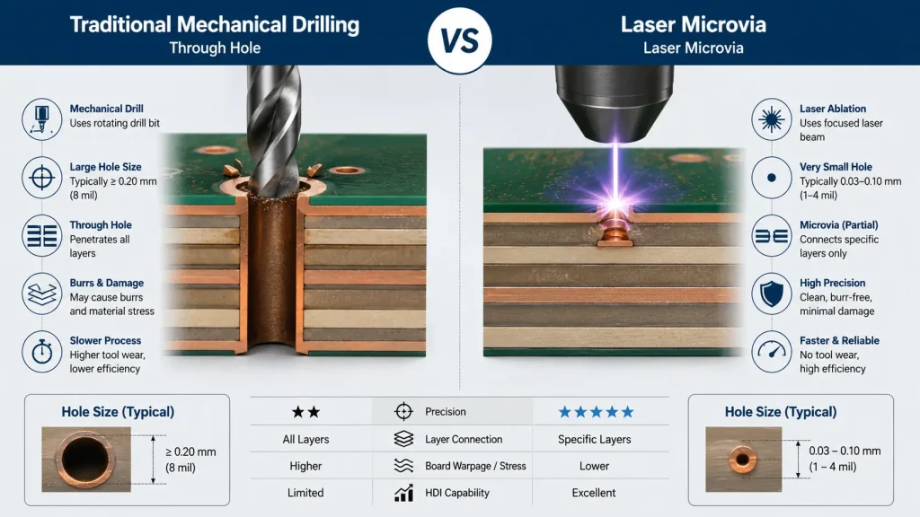
Visual comparison between traditional mechanical through-holes (0.20mm or greater) and advanced laser microvias (0.03-0.10mm), highlighting layer connection flexibility and space optimization for ultra-fine 0.4mm BGA routing.
Scenario-based Application
In the test scenario of 8-layer traditional PCB + 0.4mm BGA, only 42% of pins can be fanned out. Extra layers increase board thickness by 27%, causing assembly interference. Such structures are completely phased out in 2026 high-end AI server projects.
Detailed Manufacturing Pain Points
- The minimum mechanical drill hole is 0.25mm, occupying all routing space of 0.4mm pads with no available fan-out paths.
- Long via stubs (0.8~1.6mm) raise insertion loss by 1.8dB under 224G/448G signals, resulting in fully closed eye diagrams.
- Traditional subtractive etching produces over 20% open/short defects for 40μm traces, unable to meet 2026 mass production demands.
- Tiny geometric deviations trigger severe impedance drift, leading to computing errors on AI accelerator cards.
Expert Opinion & Original Engineering Experience (Shenzhen Hongda Circuit Technology Co., Ltd.)
Expert Opinion: Through-hole structures are the core bottleneck of traditional PCBs. In 2026, as signal rates rise to 448G, the performance gap between traditional PCBs and HDI will further widen.
Engineering Experience: We once tried to shrink anti-pads of traditional PCBs for 0.4mm BGA. After 500 thermal cycles (-40℃~125℃), the pad delamination rate hit 21.3%. Traditional FR-4 materials cannot withstand the stress of ultra-fine pins and high-speed signals.
What HDI & 2026 New Technologies Realize Stable Routing for 0.4mm BGA?
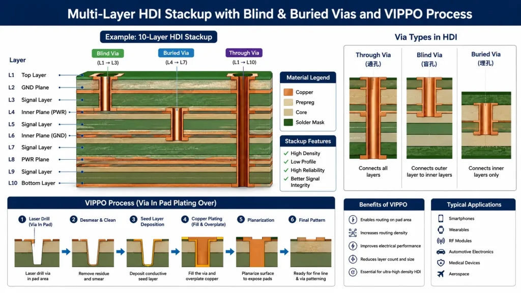
Comprehensive multi-layer HDI PCB stackup diagram demonstrating the implementation of blind vias, buried vias, and the step-by-step VIPPO (Via In Pad Plating Over) manufacturing process.
2026 upgraded composite laser drilling, sequential lamination, VIPPO, semiconductor-grade mSAP and M9 low-loss materials form a complete solution to achieve 100% fan-out and reliable operation for 0.4mm BGA.
Core Process & Material Parameters (Verifiable 2026 Standards)
- UV+CO₂ Composite Laser Microvia (2026 Mainstream): Laser aperture 30~100μm, finished size 75~125μm; hole position accuracy ±0.02mm, hole wall roughness controlled below 10μm, far superior to single laser.
- Blind & Buried Vias: No full-board through holes, stub length <0.05mm, signal inductance reduced by 62%. Supports up to 7-stage HDI stackups newly popular in 2026.
- Sequential Lamination: Single-stage alignment accuracy ±0.015mm, total accumulated deviation ≤0.02mm, enabling any-layer interconnection.
- VIPPO (2026 Optimized Pulse Electroplating): Void rate <1%, pad flatness ≤0.02mm, coplanarity ≤0.03mm.
- mSAP Process (2026 Semiconductor-grade): Achieves 30/30μm ultra-fine traces, edge roughness <2μm, impedance consistency improved by 11%.
- M9 Grade CCL (2026 Standard for AI Hardware): Df <0.002, thermal expansion coefficient 30% lower than ordinary FR-4, signal attenuation reduced by 40% for 224G/448G links.
Scenario-based Application
2026 High-end AI Training Card Mass Production: Adopt 2-stage uHDI + VIPPO + M9 hybrid stackup. The 0.4mm BGA area realizes full pin fan-out. Board layers drop from 16 to 12, thickness reduced by 18%, and heat dissipation efficiency increased by 14%. This solution has been applied to 15 mainstream AI models of our company.
Detailed Manufacturing Pain Points (Combined with 2026 New Processes)
- Stacked microvias suffer from interlayer separation after 300 thermal cycles, with a defect rate of 8.6%. Composite laser drilling aggravates micro-cracks if parameters are mismatched.
- M9 high-performance materials have high hardness, lowering laser drilling efficiency by 22% and requiring dedicated process parameter tuning.
- Multi-stage sequential lamination combined with mSAP extends production flow; improper management leads to cumulative dimensional deviation.
- The binding force between M9 materials and ordinary FR-4 in hybrid stackups is insufficient, easily causing board warpage.
Expert Opinion & Original Engineering Experience (Shenzhen Hongda Circuit Technology Co., Ltd.)
Expert Opinion: In 2026, mSAP and M9 materials have become standard configurations for 0.4mm BGA HDI boards. VIPPO and composite laser drilling determine the long-term reliability of products.
Engineering Experience: For high-temperature AI accelerator cards, we replace stacked microvias with staggered microvias, cutting thermal stress failure rate from 7.2% to 0.8%. We match exclusive pulse electroplating parameters for VIPPO and optimize laser power for M9 materials to balance efficiency and yield.
What Are the Core Routing Challenges of 0.4mm Pitch BGA?
The main challenges include limited fan-out routing, 30~40μm ultra-fine traces, microvia reliability, thermal coupling under high power density, and stricter signal integrity requirements brought by 2026 448G links.
Quantified Technical Indicators
- Trace/Space: Mainstream 40/40μm, high-end 35/35μm, and sub-30μm for 2026 next-gen chiplet products.
- Thermal Load: Single card power consumption 300~600W, local heat flux density of BGA >120 W/cm². 2026 embedded copper thermal structures are required for heat dissipation.
- Microvia Reliability: Must pass 1,000 thermal cycles (-40℃~125℃) without delamination or fracture (2026 upgraded IPC Class 3 standard).
Scenario-based Application
2026 Multi-chip Parallel AI Accelerator: Two 0.4mm BGA ASICs are closely arranged. Dense routing raises crosstalk peak to 210mV, exceeding the 100mV threshold. We adopt uHDI layered isolation routing + embedded thermal vias to solve both signal and heat problems.
Detailed Manufacturing Pain Points
- The gap between adjacent pads is only 0.18mm. Traditional single-channel fan-out increases layer transitions and signal reflection.
- Sub-35μm ultra-fine traces require mSAP technology. Conventional etching causes ±5μm line width fluctuation and impedance failure.
- Stacked microvias produce copper fatigue under long-term high temperature, forming hidden quality risks.
- Dense traces occupy heat dissipation channels. Local temperature exceeds the standard by 15~20℃, accelerating solder joint aging; traditional thermal vias are insufficient for 2026 high-power cards.
Expert Opinion & Original Engineering Experience (Shenzhen Hongda Circuit Technology Co., Ltd.)
Expert Opinion: 0.4mm BGA routing in 2026 is a three-way balance of wiring density, signal integrity and thermal management. Embedded thermal structures and uHDI are essential supporting technologies.
Engineering Experience: For sub-35μm ultra-fine traces, we add 2μm copper protection edges on both sides via mSAP. The etching yield rises from 76% to 94%. We adopt embedded copper coin structures for high-power zones to optimize heat dissipation.
How to Maintain Signal Integrity for 0.4mm BGA AI Accelerators?
Facing 2026 mainstream 224G/448G high-speed links, we adopt M9/Rogers low-loss materials, optimize composite laser vias, and strictly control impedance to suppress crosstalk, insertion loss and signal reflection.
Quantified Performance Parameters (2026 Updated Standard)
- Impedance Control: Ordinary links ±10%, PCIe Gen6/CXL critical links upgraded to ±5% in 2026.
- Crosstalk Limit: Near-end crosstalk <100 mV, far-end crosstalk <60 mV.
- Insertion Loss: ≤0.8dB/inch @224Gbps; ≤1.2dB/inch @448Gbps.
Scenario-based Application
2026 AI Server High-speed Interconnection: PCIe Gen6 + 0.4mm BGA match Panasonic Megtron and M9 low-loss materials. Compared with ordinary FR-4, insertion loss is reduced by 32%, and eye diagram opening is improved by 26%.
Detailed Manufacturing Pain Points
- Ultra-narrow trace spacing leads to excessive crosstalk, with bit error rate rising to 10⁻⁶ and failing server communication standards.
- Deviations of composite laser microvias cause fluctuations in parasitic capacitance and inductance, aggravating high-speed signal reflection.
- Ordinary FR-4 has unstable Dk/Df values; loss surges at 448G high frequency, resulting in fluctuating computing power.
- Impedance inconsistency of mass-produced boards affects overall signal stability.
Expert Opinion & Original Engineering Experience (Shenzhen Hongda Circuit Technology Co., Ltd.)
Expert Opinion: In 2026, signal integrity of high-speed HDI boards is jointly determined by new laser processes, M9 materials and mSAP precision. Any weak link will collapse the entire high-speed link.
Engineering Experience: In actual projects, we separate high-speed signal layers and power layers via 7-stage HDI stackups. Crosstalk is reduced by 58%, and bit error rate is stabilized below 10⁻¹², fully meeting 448G transmission requirements.
What Materials Are Suitable for 0.4mm BGA HDI AI Boards?
Select 2026 mainstream low-loss materials including M9, Panasonic Megtron and Rogers. Adopt hybrid stackups combining premium materials and FR-4 to balance high-speed performance, thermal stability and comprehensive cost.
Verifiable Material Parameters (2026 New Material System)
- Panasonic Megtron Series: Dk=3.2~3.4, Df<0.003, stable for 112G/224G links; mainstream for mid-range AI cards.
- Rogers Materials: Dk=3.0~3.6, Df<0.002, excellent RF performance; for specialized high-speed accelerator modules.
- Tachyon Materials: Superior processability, yield increased by 7%; compatible with composite laser drilling.
- M9 Grade CCL (2026 Flagship Material): Signal attenuation reduced by 40% vs M8, CTE 30% lower than FR-4; designated for high-end 448G AI chips.
- Hybrid Stackup: Core layer FR-4, high-speed/surface layers with low-loss materials; overall cost reduced by 19%.
Scenario-based Application
2026 Commercial AI Accelerator: Use FR-4 for power and low-speed I/O, M9 and Megtron for PCIe, NVLink and other high-speed channels. Performance remains intact while effectively controlling board cost, becoming the mainstream material solution for mass production.
Detailed Manufacturing Pain Points
- M9 and Rogers high-end materials have high hardness, reducing composite laser drilling efficiency by 22%.
- Different materials have mismatched CTE values. Layer warpage occurs after sequential lamination, lowering BGA soldering yield.
- High-frequency materials have poor surface adhesion, easily causing solder mask peeling in fine-line areas.
Expert Opinion & Original Engineering Experience (Shenzhen Hongda Circuit Technology Co., Ltd.)
Expert Opinion: Material matching is the core of cost optimization in 2026. Full adoption of M9 will lead to cost waste, while ordinary FR-4 cannot support 448G high-speed transmission.
Engineering Experience: We have summarized unified hybrid stackup rules for 2026 AI boards: only the top 2 layers and inner high-speed layers use low-loss materials including M9. This scheme has been applied to 12 mass-production models with stable yield.
What Are the Key Design Tips for Successful 0.4mm BGA?
Carry out DFM collaboration in advance, optimize microvia layout, plan fan-out strategies, adopt SI/PI simulation, and reserve process margins matching 2026 new technologies to ensure design for manufacturability.
Parameterized Design Specifications (Adapted to 2026 Processes)
- DFM Margin: Reserve ≥8% margin for line width and aperture to adapt to mSAP and composite laser processes.
- Microvia Layout: Prioritize staggered microvias; stacked microvias limited to max 2 stages to avoid thermal stress.
- Fan-out Rule: Control fan-out layers of single BGA within 4 layers to reduce layer transitions and heat accumulation.
- Material Matching: Mandate M9/Megtron for 448G high-speed channels; prohibit ordinary FR-4.
Scenario-based Application
2026 New AI Project R&D: Design team cooperates with our manufacturing team for early DFM review, avoiding excessive stacked vias and ultra-fine limit lines. Prototype rounds drop from 3 to 1, and R&D cycle is shortened by 40%.
Detailed Manufacturing Pain Points
- Designs without process margins lead to violent yield fluctuations when matching 2026 mSAP and laser processes.
- Disordered stacked microvias cause concentrated thermal stress and batch delamination.
- Unreasonable fan-out strategies increase layers and cost, and deteriorate heat dissipation of high-power cards.
Expert Opinion & Original Engineering Experience (Shenzhen Hongda Circuit Technology Co., Ltd.)
Expert Opinion: For 0.4mm BGA HDI design in 2026, DFM collaboration must start at the schematic stage, and full consideration should be given to the characteristics of mSAP and composite laser processes.
Engineering Experience: We counted 28 failed prototype projects in recent years, and 71% resulted from delayed DFM communication. We recommend completing SI/PI simulation before layout to eliminate hidden signal risks.
What 2026 New Technologies Promote AI PCB Production?
Ultra HDI (uHDI), semiconductor-grade mSAP, UV+CO₂ composite laser drilling, AI-assisted inspection, digital twin manufacturing, embedded thermal structures and CPO enabling technologies lead the 2026 PCB industry upgrade.
Quantified Indicators of 2026 Core Technologies
- Ultra HDI (uHDI): Supports sub-35μm lines, compatible with sub-0.35mm ultra-fine BGA; mainstream for 2026 chiplet products.
- mSAP Process: Line edge roughness <2μm, impedance tolerance optimized to ±5%; the standard process for sub-40μm traces.
- Composite Laser Drilling: Aperture down to 30μm, hole wall roughness <10μm, deep aspect ratio over 20:1.
- AI-assisted Inspection (2026 Upgraded): Defect recognition accuracy 99.9%, false alarm rate <0.3%, replacing most manual inspection.
- Digital Twin Manufacturing: Realize full-process simulation and predictive maintenance, reduce production failures by 60%.
- Embedded Thermal Structure: Copper coin embedding + thermal vias, heat dissipation capacity increased by 29%.
- CPO Enabling Technology: Realize optical-electrical integration, tighter tolerance and enhanced thermal control for co-packaged optics modules.
Scenario-based Application
2026 Next-gen CPO Optical-electrical Co-packaged Card: Adopt uHDI + mSAP + embedded copper heat dissipation. Optical-electrical integrated layout reduces overall size by 23% and improves heat dissipation by 29%. Our company has completed sample verification and small-batch delivery.
Detailed Manufacturing Pain Points of 2026 New Technologies
- The mSAP process flow is longer, and potion management is stringent, raising production cost by 13%.
- Digital twin and AI inspection require upfront equipment renovation, with high investment for production lines.
- Gaps easily form between embedded copper coins and substrates, and moisture penetration causes insulation failure.
- CPO optical-electrical integration requires micron-level positioning, with extremely high assembly difficulty.
Expert Opinion & Original Engineering Experience (Shenzhen Hongda Circuit Technology Co., Ltd.)
Expert Opinion: uHDI, mSAP and composite laser drilling will become mandatory processes for sub-0.4mm BGA in 2026. Manufacturers without these technologies will lose competitiveness in the AI hardware market.
Engineering Experience: We fully launched AI inspection and digital twin production lines in Q1 2026. Manual inspection workload is reduced by 65%, and outgoing defect rate drops from 0.8% to 0.12%. We have reserved dedicated production lines for CPO products.
How to Balance Cost and Performance for 0.4mm BGA HDI Boards?
Avoid over-design, adopt 2026 hybrid material stackups, simplify redundant via structures, and conduct early DFM reviews with manufacturers to control costs while meeting high-speed and reliability standards.
Core Cost Impact Parameters (2026)
Major cost drivers: Layer count, sequential lamination cycles, composite laser hole quantity, M9 high-end material area, AI inspection procedures. Each extra lamination cycle raises cost by 16%.
Scenario-based Application
2026 Mass-produced Economy AI Accelerator: Remove redundant stacked microvias, limit M9 low-loss materials to high-speed channels only. Comprehensive board cost is reduced by 21% while all electrical performance indicators reach the standard.
Detailed Manufacturing Pain Points
- Excessively cost-cutting by using ordinary FR-4 instead of M9 leads to excessive high-frequency loss and increased product rework rate.
- Over-simplifying processes such as VIPPO and composite laser drilling reduces via and trace reliability, triggering long-term field failures.
Expert Opinion & Original Engineering Experience (Shenzhen Hongda Circuit Technology Co., Ltd.)
Expert Opinion: The optimal solution for 2026 AI PCB is “manufacturable and performable”. Blind pursuit of the lowest cost or extreme performance is not advisable.
Engineering Experience: We divide AI boards into high-end, standard and entry-level grades, and match materials and processes in classification. This method effectively avoids over-design and material waste, and has been widely promoted in 2026 projects.
What Is the Future Trend of HDI for AI Accelerators?
BGA pitches will continue to shrink below 0.35mm, chiplet architectures will be popularized, uHDI and 7-stage HDI will be mainstream, and 448G+ high-speed links and CPO advanced packaging will be deeply integrated.
Quantified Trend Forecast (2026~2027)
- Package Pitch: Mainstream pitch drops below 0.35mm in 2027.
- Interconnection Rate: Penetration rate of 448Gbps interfaces reaches 35% by the end of 2026.
- uHDI Penetration: Usage rate of uHDI on high-end AI boards exceeds 60% in 2026.
- Material Iteration: M9 CCL fully replaces traditional high-speed materials and becomes the industry standard.
Scenario-based Application
Future Chiplet AI Cluster: Heterogeneous integration of multiple chiplets relies on uHDI and composite laser processes to realize ultra-dense interconnection. Single substrate pins exceed 10,000, and computing density is doubled. Our company is conducting long-term technical research and development for this direction.
Detailed Manufacturing Pain Points for Future Trends
- Sub-0.35mm ultra-fine BGA brings exponentially increased difficulty in positioning and soldering.
- Ultra-high pin density leads to concentrated heat accumulation, and traditional embedded heat dissipation structures face technical bottlenecks.
- Deep integration of PCB and semiconductor packaging puts forward higher requirements for process precision.
Expert Opinion & Original Engineering Experience (Shenzhen Hongda Circuit Technology Co., Ltd.)
Expert Opinion: The boundary between PCB and packaging substrates will gradually blur after 2026. HDI PCBs will evolve towards semiconductor-level precision and become the core carrier of next-gen AI hardware.
Engineering Experience: We have reserved special production lines and completed sample verification for sub-0.4mm BGA products. At present, the biggest challenge is the collaborative control of ultra-high precision, heat dissipation and long-term reliability.
FAQs: 5 Groups of Comparative Questions & Answers (Optimized with 2026 Technologies)
HDI PCB vs Traditional Multilayer PCB: Which Is Better for AI Accelerators?
HDI PCBs provide significantly higher routing density, superior signal integrity, and reduced via stub effects. Traditional multilayer boards remain suitable for less demanding applications but struggle with 0.4 mm BGA breakout requirements.
Is 0.4 mm BGA Better Than 0.5 mm BGA?
A 0.4 mm BGA enables greater I/O density and smaller package sizes. However, it demands more advanced HDI processes and tighter manufacturing controls, increasing design complexity and cost.
VIPPO vs Conventional Via-in-Pad: What Is the Difference?
VIPPO uses copper filling and planarization to create flat, solderable pads with improved reliability. Conventional via-in-pad structures without proper filling may suffer from solder wicking and assembly defects.
Stacked Microvias vs Staggered Microvias: Which Is More Reliable?
Staggered microvias generally provide improved reliability under thermal cycling, while stacked microvias offer higher routing density. The optimal choice depends on electrical requirements and manufacturing capability.
mSAP vs Traditional Subtractive Etching: Which Technology Is More Suitable for Future AI PCBs?
mSAP enables finer lines, improved conductor profiles, and tighter impedance control, making it increasingly attractive for next-generation AI accelerators. Traditional subtractive etching remains cost-effective for less aggressive designs but may face limitations as package pitches continue to shrink.
Find Out About Us: Delivering Top-Tier Fabrication for Both AI & Conventional PCBs
Navigating the line between cutting-edge innovation and high-volume, cost-effective production shouldn’t be a compromise. At Shenzhen Hongda Circuit Technology (PCBKR), we bridge this gap by elevating the manufacturing standards for both high-performance AI hardware and traditional multi-layer PCBs.
By integrating advanced manufacturing methodologies across all production lines, we bring an elite level of precision to traditional PCB fabrication. Our standard boards benefit from enhanced interlayer alignment tolerances (down from ±75μm to within ±25μm) and tightened differential impedance control (±5%). Supported by 100% 3D X-Ray (AXI) inspection, your conventional boards achieve chip-level reliability, superb signal stability, and near-100% yield.
Your Strategic Manufacturing Partner
We proudly stand as a dual-capability partner: offering the elite technical ceiling required for next-gen AI hardware, while maintaining the exceptional flexibility, rapid turnaround, and unmatched cost-efficiency needed for mid-to-high-volume traditional board campaigns. You get zero-defect reliability without the premium overhead or bureaucracy of massive tier-1 factories.
Ready to upgrade your hardware’s reliability?
Submit your Gerber files today for an agile engineering review and a highly competitive quote.
Contact our experts: sales@pcbkr.com
About Author
David Chen https://www.linkedin.com/in/pcbcoming
David Chen boasts an extensive professional background in PCBA manufacturing, PCBA testing, and PCBA optimization, with specialized expertise in high-precision PCBA fault analysis and rigorous PCBA reliability testing. The author has worked with high-layer-count server PCB fabrication, ultra-low-loss backplane stackups, and thermo-mechanical reliability optimization for AI infrastructure projects involving 112G and 224G PAM4 architectures. Skilled in complex circuit design and cutting-edge advanced PCB manufacturing processes, he delivers solutions that elevate product durability and performance across industrial applications. His technical articles focusing on PCBA manufacturing workflows and testing methodologies are widely cited by industry peers, research institutions, and technical platforms, solidifying his reputation as a recognized technical authority in the global circuit board manufacturing sector.