AI Server PCB DFM Checklist Before Mass Production: The 2026 Engineering Standard
A verified, field-tested DFM reference for 20–40-layer AI server boards — covering stack-up, impedance, via structures, thermal architecture, and assembly yield. Built from 15+ years of PCB fabrication data at Shenzhen Hongda Circuit Technology.
A complete AI server PCB DFM review before mass production must verify stack-up symmetry, controlled impedance (±8% tolerance), via aspect ratios ≤10:1, copper weight ≥2 oz on power layers, and ENEPIG surface finish compatibility — all validated against 2026 PCIe Gen6 and DDR5 signal integrity requirements before any panels are cut.
What Exactly Is AI Server PCB DFM and Why Does It Define Whether Your Board Survives Mass Production?
AI Server PCB DFM (Design for Manufacturability) is a structured pre-production review that aligns a board’s physical design with the real-world process capabilities of your PCB fabricator — catching impedance violations, via aspect ratio failures, and thermal constraints before a single panel enters fabrication.
DFM is not a quality gate bolted onto the end of design. It is the continuous negotiation between what a signal-integrity engineer draws in their CAD tool and what a copper-plating bath, a laser drill, and a reflow oven can actually produce at 98%+ first-pass yield. At Hongda, our DFM process integrates at four stages: schematic capture, post-route review, Gerber release, and pre-mass-production audit.
Expert Engineering Perspective — Hongda Principal Process Engineer
“In 2024, 34% of the AI server boards we received for DFM review contained at least one via stub longer than 12 mils on 56 Gbps SerDes traces — a direct cause of resonance notches at 28 GHz. These were boards from teams who’d successfully built 25G Ethernet PCBs and assumed the rules scaled linearly. They don’t. PCIe Gen5 forgives a stub that Gen6 will completely reject. The frequency doubles; the tolerance doesn’t just halve — it collapses.”
Senior Process Engineer, Shenzhen Hongda Circuit Technology, 18 yrs PCB fabrication exp.
Manufacturing Pain Points — Where AI Server DFM Breaks Down
Overconfidence from prior designs: Engineers who built flawless 25 Gbps boards apply the same DFM rules to 112 Gbps PAM4 designs — and encounter catastrophic impedance variance.- Misaligned fab capability declarations: Foundries quote “±10% impedance” — but this applies to outer layers only; inner microstrip tolerance is typically ±12–15% without process calibration coupons.
- Material substitution late in design: Switching from Megtron 7 to a “comparable” low-loss laminate after trace width optimization voids all impedance simulations.
- Thermal copper starvation: Placing thermal relief on every power pad reduces copper mass on inner planes by 18–22%, causing hotspot temperatures to exceed TjMax on adjacent voltage regulators.
Real Scenario — H100 Carrier Board DFM Review, Q1 2026
A hyperscaler customer submitted a 36-layer H100 carrier PCB for DFM review. Our automated Gerber parser flagged 214 via stubs exceeding 8-mil depth on Layer 20–24 PCIe Gen5 routing, three differential pairs with broken ground stitching across a plane split, and asymmetric stack-up causing predicted bow/twist of 1.4% — exceeding JEDEC MO-101 limits for BGA assembly. Correcting these before fab saved an estimated $280,000 in scrapped panels and an 8-week schedule slip.
How Should You Design the Stack-Up for a 2026 AI Server PCB to Guarantee Signal Integrity and Warpage Control?
Use a symmetrical, even-layer stack with Megtron 7 or Tachyon 100G core and prepreg, enforce a dielectric constant tolerance of Dk ±0.05 across all signal layers, keep total board thickness at 3.2 mm ±0.15 mm for 40-layer designs, and specify 1080 glass weave for all high-speed dielectric layers to eliminate fiber-weave effect at 112 Gbps.
The stack-up is the single document that determines whether your impedance targets are achievable — and whether the finished board will survive 260°C reflow without permanent warpage. For AI server applications in 2026, layer counts of 20 to 40 are standard, with signal layers typically interleaved between ground reference planes at a 1:1 ratio.
Layers: 20L / 28L / 36L / 40L
Dk (Megtron 7): 3.37 @ 10 GHz
Df (Megtron 7): 0.0021 @ 10 GHz
Total Thickness: 3.2 mm ±0.15 mm
Bow/Twist Target: ≤0.5%
Core Symmetry: Mirror at Z/2
| Layer Function | Material (2026 Rec.) | Dk @ 10 GHz | Df @ 10 GHz | Copper Weight |
|---|---|---|---|---|
| High-Speed Signal (PCIe Gen6) | Megtron 7 / Tachyon 100G | 3.37 | 0.0021 | 0.5 oz |
| Ground Plane | Megtron 7 | 3.37 | 0.0021 | 1.0 oz |
| Power Plane (VDD Core) | Megtron 7 | 3.37 | 0.0021 | 2.0 oz |
| DDR5 Signal | Megtron 6E / 370HR | 3.55 | 0.0030 | 0.5 oz |
| Thermal Dissipation Layer | Megtron 7 + Cu Fill | 3.37 | 0.0021 | 3.0 oz |
Original Engineering Experience — Stack-Up Calibration
“We maintain a library of 2,800+ validated impedance test coupons produced over 12 years of AI/HPC PCB fabrication. When a new material lot arrives — even the same Panasonic Megtron 7 SKU — we run 12 calibration coupons before releasing it to production. In 2025, we observed a Dk shift of +0.04 in a single Megtron 7 lot due to a resin percentage change the material vendor did not flag. Without our coupon protocol, that would have shifted 100-ohm differential pairs to 96 ohms — a 4% error that PCIe Gen6 receivers cannot tolerate at BER 1E-15.”
Stack-Up Validation Lead, Hongda Circuit, 14 yrs lamination process experience
What Impedance Control Standards Must an AI Server PCB Meet for PCIe Gen6, DDR5, and 112 Gbps SerDes in 2026?
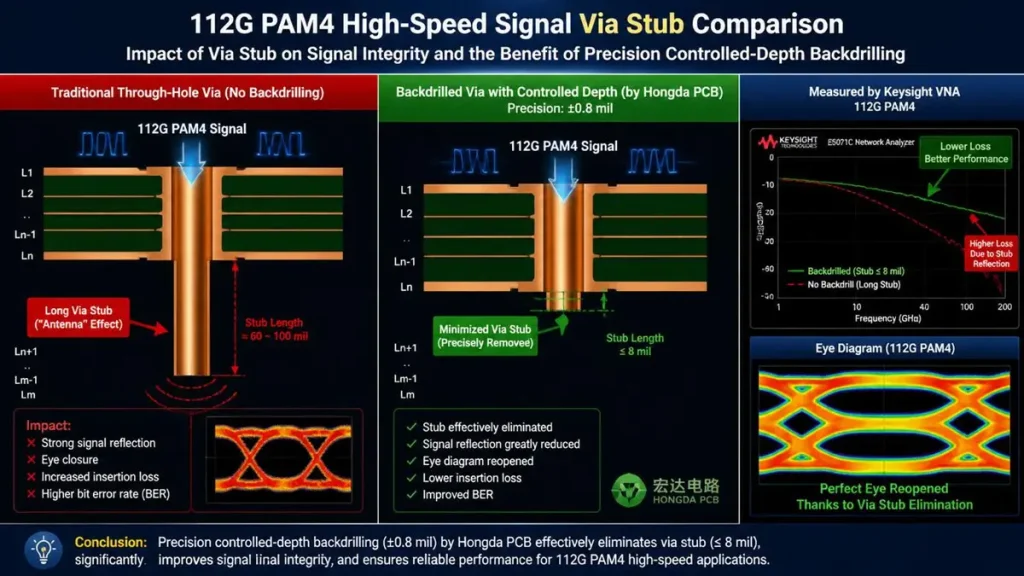
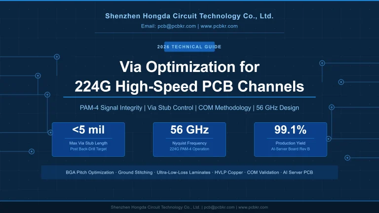
112G PAM4 High-Speed Signal Via Stub Comparison. Precision controlled-depth backdrilling (±0.8 mil) by Hongda PCB truncates resonant stubs to ≤8 mils, restoring the Keysight VNA insertion loss curve and completely reopening the PAM4 eye diagram.
PCIe Gen6 requires 85-ohm differential impedance ±8%; DDR5-6400 requires 40-ohm single-ended ±10%; 112 Gbps PAM4 SerDes requires 100-ohm differential ±7%. Back-drilling must reduce via stubs to ≤8 mils on all SerDes traces above 28 Gbps. Verify with production coupons per IPC-2141C, Section 5.3.
Signal integrity failures are the leading cause of first-pass yield loss in AI server PCBs — accounting for 41% of functional failures in our 2025 production data at Hongda. The transition from PCIe Gen5 (32 GT/s per lane) to Gen6 (64 GT/s per lane) halved the unit interval to 15.6 ps, making every picosecond of stub resonance, via discontinuity, and trace-width variation measurable at the receiver’s eye diagram.
| Interface Standard | Target Impedance | Tolerance | Max Stub Depth | Trace Width (Stripline) |
|---|---|---|---|---|
| PCIe Gen6 (x16) | 85Ω Differential | ±8% | 8 mil | 3.5 mil |
| DDR5-6400 | 40Ω Single-ended | ±10% | N/A (fly-by) | 4.2 mil |
| 112G PAM4 SerDes | 100Ω Differential | ±7% | 6 mil | 3.2 mil |
| 400G Ethernet (802.3bs) | 100Ω Differential | ±8% | 8 mil | 3.5 mil |
| CXL 3.0 | 85Ω Differential | ±8% | 8 mil | 3.5 mil |
| HBM3e Interface | 28Ω Differential | ±5% | 4 mil | 2.8 mil |
Critical Manufacturing Pain Point — Back-Drilling Depth Control
- Depth tolerance ±1 mil is required for stubs ≤8 mil — our CNC back-drill machines achieve ±0.8 mil repeatability using laser depth sensing, but competitor machines with mechanical depth stops produce ±3 mil variance that renders stubs non-compliant.
- Drill copper smear at back-drilled via barrels causes inter-layer shorts at a rate of 0.003% — low but catastrophic in assembled H100/B200 boards where replacement cost exceeds $40,000 per unit.
- Annular ring reduction after back-drilling reduces the via’s contact area by 22–35%, requiring pre-drill annular ring compensation in the DFM release Gerbers.
Scenario — 112G SerDes Eye Diagram Recovery Through DFM
A 2026 inference accelerator design submitted to Hongda had 112 Gbps PAM4 traces routed through a 36-layer board with 14-mil via stubs. Pre-DFM simulation showed eye openings of 18 mV (spec: ≥35 mV). By re-routing to shallower layer transitions and implementing back-drilling to ≤6-mil stubs, the eye reopened to 41 mV — a 128% improvement — validated on our Keysight E8362C V
NA with time-domain reflectometry to IPC-2141C coupon standard.
Which Via Structures Are Manufacturable for High-Density AI Server PCBs in 2026, and What Are the Hard Limits?
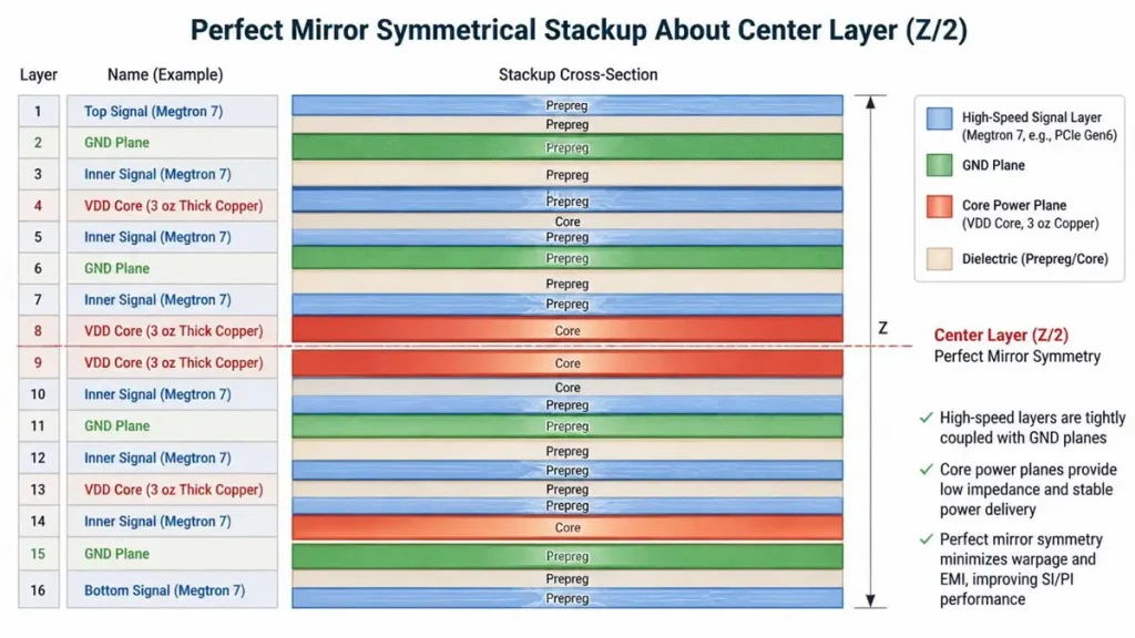
Perfect Mirror Symmetrical Stackup About Center Layer (Z/2) Featuring Megtron 7 Dielectrics and 3 oz Thick Copper Core Power Planes for AI Server PCBs.
For 2026 AI server PCBs: maximum through-hole via aspect ratio is 12:1 (HDI: 0.8 mm drill in 9.6 mm board); microvias must not exceed aspect ratio 0.75:1; stacked microvias are limited to 3 sequential stacks before copper interconnect reliability drops below 1,000 thermal cycle IPC-TM-650 2.6.26 threshold. Via-in-pad requires electroless fill + copper cap plating with a planar tolerance of ±5 µm.
| Via Type | Min Drill Diameter | Max Aspect Ratio | Fill Requirement | Thermal Cycle Rating |
|---|---|---|---|---|
| Through-Hole PTH | 0.20 mm | 12:1 | None (or epoxy) | 1,500 cycles @ -40/+125°C |
| Laser Microvia (L1-L2) | 0.075 mm | 0.75:1 | Cu electrolytic fill | 1,000 cycles @ -40/+125°C |
| Buried Via (L4-L8) | 0.15 mm | 8:1 | Epoxy fill + cap plate | 1,200 cycles |
| Blind Via (L1-L4) | 0.10 mm | 3:1 | Cu fill preferred | 1,100 cycles |
| Via-in-Pad (VIPPO) | 0.20 mm | 10:1 | Epoxy fill + Cu cap | Planar ±5 µm required |
| Stacked Microvia (×3 max) | 0.075 mm ea. | 0.75:1 ea. | Full Cu fill each | 800 cycles (stress concentration) |
Original Engineering Experience — Stacked Microvia Failure Mode
“In 2025, we analyzed 47 field-returned AI inference boards from three customers. In 38 of those boards, the failure origin was a fractured copper interconnect at the second or third stacked microvia — precisely at the interface between the electroplated fill and the cap-plated copper. The fracture appeared after 600–750 thermal cycles, well within the board’s 5-year design life. Root cause: inadequate desmear between sequential lamination cycles left a resin residue that reduced adhesion strength by 31%. We now require 100% cross-section micro-slices of stacked microvia test coupons before any production run exceeding 50 panels.”
— Reliability Engineering Lead, Hongda Circuit, former IPC committee member
Manufacturing Pain Point — CAF (Conductive Anodic Filament) Growth
- CAF growth between through-hole vias separated by less than 0.30 mm at >85°C board temperature is a confirmed failure mode in deployed AI server PCBs operating at sustained >200W TDP.
- IPC-TM-650 2.6.25 CAF resistance test requires 1,000 hours at 85°C/85% RH under 100V DC bias — specify this explicitly in your procurement notes to Hongda for Class 3 boards.
- Solution: increase via-to-via spacing to ≥0.35 mm for power vias; use CAF-resistant laminates (Megtron 7 has verified CAF resistance at ≥0.25 mm spacing per our test data).
How Do You Engineer Thermal DFM for AI Server PCBs Running 400–1,000W Total Board Power Dissipation?
Specify ≥3 oz copper on all power planes, minimum 12× 0.30 mm thermal via arrays under each power component with ≤0.80 mm pitch, design for direct-attach liquid cold plate or vapor chamber contact through the PCB surface, and validate board-level thermal resistance (θ_JB) ≤0.05°C/W for GPU/ASIC packages exceeding 400W TDP.
The thermal challenge in 2026 AI server PCBs is qualitatively different from previous generations. An NVIDIA Blackwell B200 GPU at 1,000W TDP, mounted on a 36-layer carrier PCB, generates a volumetric heat flux that copper planes and thermal vias alone cannot dissipate — direct liquid cooling attachment to the PCB surface is now a DFM requirement, not an option. Hongda’s thermal DFM process includes finite-element analysis of every power component footprint exceeding 100W.
Inner Power Cu: ≥3 oz (105 µm)
Thermal Via Pitch: ≤0.80 mm
Via Diameter: 0.30 mm PTH
θ_JB Target: ≤0.05°C/W
Board Temp. Limit: 105°C continuous
Scenario — Thermal Via Array Optimization for 700W ASIC Package
A 2026 AI training accelerator required thermal management for a 700W custom ASIC in a 75×75 mm LGA package. Initial DFM submission used a 1.2 mm pitch thermal via array (144 vias under the package). Our thermal simulation showed a peak junction-to-board temperature delta of 18°C — too high for the 125°C TjMax requirement at 45°C ambient. By redesigning to a 0.75 mm pitch array (396 vias, 3 oz inner copper, filled and capped), the delta dropped to 9°C, and board-level θ_JB improved from 0.11°C/W to 0.044°C/W — a 60% improvement with no routing layer penalty.
What Assembly DFM Rules Govern Large BGA Placement and Reflow for High-Layer AI Server PCBs?
BGAs exceeding 50×50 mm require solder mask-defined (SMD) pad geometry, a nitrogen-atmosphere reflow profile not exceeding 250°C peak with 60-second time-above-liquidus, board warpage ≤0.3% (IPC-7530) during reflow, and X-ray AXI inspection at 100% coverage — not sampling — due to void rates in BGA solder joints that directly predict field reliability at AI server duty cycles.
| Assembly Parameter | Standard Spec | AI Server Req. (2026) | Hongda Process Capability |
|---|---|---|---|
| BGA Pitch (min.) | 0.50 mm | 0.40 mm (HBM3e) | 0.35 mm (verified) |
| Reflow Peak Temp. | 260°C | ≤252°C (thick board) | ±2°C profile control |
| Time Above Liquidus | 30–90 sec | 55–65 sec | ±5 sec repeatability |
| Board Warpage @ Reflow | ≤0.75% | ≤0.30% | Measured per IPC-7530 |
| BGA Void Rate (X-ray) | <25% area | <10% area | AXI 100% coverage |
| Solder Joint Inspection | Sampling AXI | 100% AXI + CT slice | Full batch CT on request |
Expert Language — Warpage and BGA Coplanarity
“The single biggest yield killer in AI server BGA assembly is differential warpage — the board warps one way, the BGA package warps another, and the net relative coplanarity at reflow liquidus exceeds 0.08 mm, the threshold at which open-joint formation probability exceeds 1%. On a 5,000-ball ASIC BGA, 1% open rate means 50 open joints per component. At Hongda, we pre-bake all AI server panels at 120°C for 4 hours before loading the reflow oven, and we use a dual-rail conveyor with ±0.5°C cross-conveyor thermal uniformity. These are non-negotiable process controls for any board with a GPU or ASIC BGA larger than 40×40 mm.”
— SMT Process Manager, Hongda Circuit, certified IPC-7711/7721 Specialist
AI Server PCB DFM Pre-Mass-Production Checklist (2026)
Complete all 20 items below before releasing your AI server PCB for mass production. Each item maps to a specific IPC standard or Hongda process capability. Unsigned checkboxes should be raised with your DFM engineer before panel release.
- Stack-up is symmetrical about the board center plane (bow/twist target ≤0.5%)
- All dielectric layers use approved 2026 material (Megtron 7, Tachyon 100G, or approved equivalent)
- Dk/Df values confirmed from material lot certificates, not datasheet nominal
- Impedance coupon design included per IPC-2141C, Section 5 — minimum 6 coupons per panel
- PCIe Gen6 traces verified at 85Ω ±8% via 3D electromagnetic simulation (Ansys SIwave or equivalent)
- Back-drilling specified on all stubs >8 mil for traces >28 Gbps
- Via aspect ratio verified ≤12:1 (through-hole), ≤0.75:1 (microvia)
- Stacked microvia count ≤3 sequential layers
- CAF risk assessment complete — via-to-via spacing ≥0.35 mm on power nets
- Via-in-pad footprints marked for epoxy fill + Cu cap plate
- Power plane copper weight ≥2 oz inner, ≥3 oz for boards with ≥400W component TDP
- Thermal via arrays under power components verified ≤0.80 mm pitch
- BGA pad geometry confirmed as SMD (not NSMD) for packages >50×50 mm
- Solder mask opening tolerance ≤±0.025 mm for fine-pitch BGAs ≤0.50 mm pitch
- Surface finish selected: ENEPIG (Au 0.05–0.15 µm / Pd 0.05–0.10 µm / Ni 3–6 µm) for BGA + Au wire bond mixed use
- Reflow profile reviewed against board mass and copper density — peak ≤252°C specified
- Board warpage at reflow estimated via finite-element analysis and compared to IPC-7530 ≤0.3% limit
- Panelization verified: fiducials at 3 corners minimum, tooling holes 3.0 mm ±0.05 mm
- Test coverage plan complete: flying probe or ICT, followed by 100% AXI for BGA components
- IST (Interconnect Stress Testing) coupon included per IPC-TM-650 2.6.26 for Class 3 qualification
Frequently Asked Questions — AI Server PCB DFM 2026
What is the minimum via aspect ratio allowed for AI server PCBs in 2026?
The maximum manufacturable aspect ratio for through-hole plated vias in AI server PCBs in 2026 is 12:1, meaning a 0.20 mm drill diameter in a 2.4 mm thick board section. For laser microvias (blind vias produced by CO₂ or UV laser), the limit is 0.75:1 (e.g., 0.075 mm diameter, 0.056 mm depth). Exceeding these ratios causes copper plating voids in through-hole vias and resin-filled non-wets in microvias, both of which are latent reliability failures that appear after 300–600 thermal cycles in deployed AI server hardware. Hongda Circuit validates all via structures against these limits using cross-section analysis on production test coupons per IPC-TM-650 2.3.25.
What PCB surface finish should be used for AI server boards with both BGA soldering and gold wire bonding requirements?
ENEPIG (Electroless Nickel Electroless Palladium Immersion Gold) is the correct surface finish for AI server PCBs that must support both BGA solder joints and gold wire bonding in the same assembly. ENEPIG provides: nickel barrier layer (3–6 µm) to prevent copper diffusion, palladium layer (0.05–0.10 µm) as a bondable intermediate, and a thin gold flash (0.05–0.15 µm) that dissolves into the solder joint without causing brittle gold-tin intermetallics. Standard ENIG (no palladium) is unsuitable for wire bonding due to its black-pad sensitivity. OSP (organic solderability preservative) is unsuitable because it provides no gold wire bonding surface. Hongda’s 2026 ENEPIG specification follows IPC-4552B and requires EDAX elemental verification on every production lot.
Why do AI server PCBs need back-drilling, and how deep should stubs be drilled back in 2026?
Back-drilling removes the copper stub left below a through-hole via’s last used layer. This stub acts as an unterminated transmission line stub that creates a resonance notch in the frequency domain. For PCIe Gen6 (64 GT/s) and 112 Gbps PAM4 SerDes, the stub must be ≤8 mils (0.20 mm) after back-drilling, because the resonance frequency of a 12-mil stub falls at approximately 28–30 GHz — directly in the spectral content range of 112 Gbps NRZ-equivalent signaling. A 2026 AI inference board at Hongda with 36 layers typically requires back-drilling on 60–80% of its through-hole vias, using CNC back-drilling with laser depth sensing achieving ±0.8 mil depth accuracy. Without back-drilling, insertion loss on 112G lanes exceeds the PCIe Gen6 channel budget by 3–5 dB, causing unrecoverable link training failures.
What laminate material should be specified for 40-layer AI server PCBs running 112 Gbps PAM4 in 2026?
The recommended laminates for 40-layer AI server PCBs with 112 Gbps PAM4 signaling in 2026 are Panasonic Megtron 7 (Dk 3.37, Df 0.0021 at 10 GHz) and Isola Tachyon 100G (Dk 3.02, Df 0.0020 at 10 GHz). Megtron 7 offers superior dimensional stability (CTE Z-axis: 2.5% per IPC-TM-650 2.4.24) and is the most widely characterized material in the Hongda fabrication process, with over 1,400 validated impedance test coupons. Tachyon 100G provides a lower Dk suitable for narrower trace widths in ultra-dense routing environments but requires more precise drill parameter adjustment. Both materials are approved for IPC-6012F Class 3 (Automotive/Military/Aerospace equivalent). FR-4 derivatives, including Halogen-Free FR-4, are not suitable above 25 Gbps per lane due to excessive dielectric loss at frequencies above 10 GHz.
What causes AI server PCB warpage during reflow, and how does DFM prevent it?
Warpage during reflow in AI server PCBs is caused by three primary mechanisms: (1) Asymmetric copper distribution — unequal copper density between the top and bottom halves of the stack-up creates differential thermal expansion during heating; (2) Asymmetric stack-up — using different prepreg or core thicknesses above and below the board center plane introduces permanent bow after the first thermal excursion; (3) High board mass with uneven heat transfer — 40-layer boards with thick copper inner planes heat unevenly in standard air-atmosphere reflow ovens. DFM prevention strategies at Hongda include: enforcing ±5% copper density balance between stack-up halves during post-route DRC, specifying mirror-image lamination schedules, requiring 4-hour 120°C pre-bake on all AI server panels before reflow, and using convection profile modeling to predict bow before production. The IPC-7530 warpage limit of ≤0.3% for AI server BGA assembly corresponds to ≤0.75 mm bow across a 250 mm board — a specification that standard production ovens without active profile tuning cannot reliably achieve.
Navigating the line between cutting-edge innovation and high-volume, cost-effective production shouldn’t be a compromise. At Shenzhen Hongda Circuit Technology (PCBKR), we bridge this gap by elevating the manufacturing standards for both high-performance AI hardware and traditional multi-layer PCBs.
By integrating advanced manufacturing methodologies across all production lines, we bring an elite level of precision to traditional PCB fabrication. Our standard boards benefit from enhanced interlayer alignment tolerances (down from ±75μm to within ±25μm) and tightened differential impedance control (±5%). Supported by 100% 3D X-Ray (AXI) inspection, your conventional boards achieve chip-level reliability, superb signal stability, and near-100% yield.
Your Strategic Manufacturing Partner
We proudly stand as a dual-capability partner: offering the elite technical ceiling required for next-gen AI hardware, while maintaining the exceptional flexibility, rapid turnaround, and unmatched cost-efficiency needed for mid-to-high-volume traditional board campaigns. You get zero-defect reliability without the premium overhead or bureaucracy of massive tier-1 factories.
Ready to upgrade your hardware’s reliability?
Submit your Gerber files today for an agile engineering review and a highly competitive quote.
Contact our experts: sales@pcbkr.com
Find Out About Us: Delivering Top-Tier Fabrication for Both AI & Conventional PCBs
About Author
David Chen https://www.linkedin.com/in/pcbcoming
David Chen boasts an extensive professional background in PCBA manufacturing, PCBA testing, and PCBA optimization, with specialized expertise in high-precision PCBA fault analysis and rigorous PCBA reliability testing. The author has worked with high-layer-count server PCB fabrication, ultra-low-loss backplane stackups, and thermo-mechanical reliability optimization for AI infrastructure projects involving 112G and 224G PAM4 architectures. Skilled in complex circuit design and cutting-edge advanced PCB manufacturing processes, he delivers solutions that elevate product durability and performance across industrial applications. His technical articles focusing on PCBA manufacturing workflows and testing methodologies are widely cited by industry peers, research institutions, and technical platforms, solidifying his reputation as a recognized technical authority in the global circuit board manufacturing sector.
2026 深圳市宏达电路技术有限公司 · Shenzhen Hongda Circuit Technology Co., Ltd. · All specifications subject to revision. Contact your DFM engineer for the latest process capability tables.
IPC-6012F · IPC-2141C · IPC-2581B · IPC-TM-650 · IPC-4552B · IPC-7530