HDI PCB Manufacturing Guide: Definition, Microvia Types, Process Capabilities, and Quality Certification
What Is HDI PCB Manufacturing?
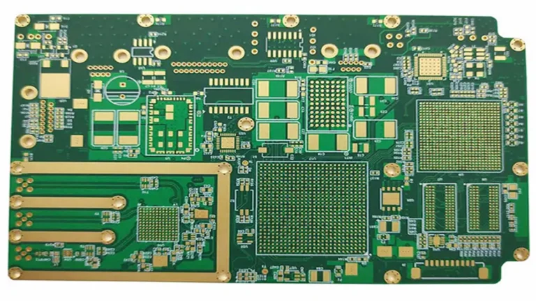
High-Density Interconnect (HDI) PCB manufacturing represents the pinnacle of contemporary printed circuit interconnect architecture. By definition, an HDI PCB is a circuit board characterized by a higher wiring density per unit area than conventional printed circuit boards. This is achieved through finer lines and spaces (≤ 3 mils / 75 µm), smaller capture pads, and the integration of microvias, blind vias, and buried vias.
The core value of HDI technology centers on spatial optimization and signal path minimization. As silicon integration drives integrated circuit (IC) pin pitches down to 0.4mm or lower, traditional through-hole drilling fails due to physical layout constraints and structural pad limitations. HDI solves this by embedding interconnects directly within functional component pads, eliminating parasitic capacitance and inductance inherent in traditional long barrel via geometries.
| Feature / Metric | Traditional Multilayer PCB | Advanced HDI PCB (2026 Standards) |
|---|---|---|
| Minimum Line / Space | ≥ 4 mils (100 µm) | ≤ 2 mils (50 µm) (mSAP capable) |
| Via Mechanical Diameter | ≥ 8 mils (200 µm) | 3–6 mils (75–150 µm) (Laser Drilled) |
| Pad-In-Product Architecture | Rare / Offset Routing Required | Standard VIPPO / Via-in-Pad |
| Signal Integrity Attenuation | Moderate to High at >28 GHz | Ultra-low Loss (Optimized for 112G/224G PAM4) |
This structural dense routing profile makes HDI mandatory for high-performance, high-frequency computing ecosystems. Typical primary application scenarios include AI server accelerator baseboards, next-generation high-speed backplanes, 4K/8K AI smart camera modules, enterprise telecommunication routing nodes, aerospace avionics, and high-density medical imaging equipment.
HDI PCB Structure and Technology Basics
HDI PCB Classic Multi-layer Stackup and Blind/Buried Vias Structure
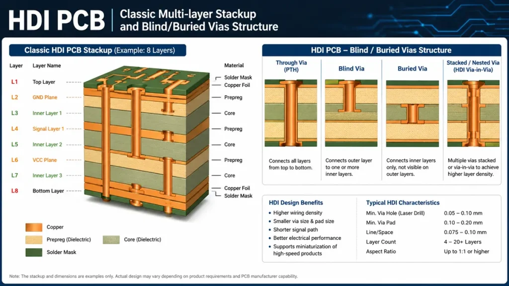
The foundational architectural unit of an HDI PCB is the build-up layer. Unlike sequential lamination where all layers are compressed simultaneously, HDI employs consecutive build-up cycles where dielectric layers and copper foils are iteratively applied over a rigid core substrate.
+-------------------------------------------------------+  [Top Layer: Outer Copper / Sm]
|   === Microvia (Blind) ===                            |  [Build-up Layer 1]
+-------------------------------------------------------+  [Build-up Layer 2]
|                       [=== Buried Via ===]            |  [Core Substrate Layer]
+-------------------------------------------------------+  [Build-up Layer 3]
|   === Microvia (Blind) ===                            |  [Build-up Layer 4]
+-------------------------------------------------------+  [Bottom Layer: Outer Copper / Sm]
To navigate this high-density layout, three via categories are utilized:
- Microvias: Vias with a diameter ≤ 6 mils (150 µm), typically traversing only one dielectric layer, formed via laser ablation.
- Blind Vias: Interconnects originating on an outer layer but terminating on an internal layer, invisible from the opposite side of the board.
- Buried Vias: Interconnects entirely contained within internal layers, passing through the core structure without penetrating either outer surface.
Implementing this interconnect matrix maximizes routing freedom. By migrating routing layers into ultra-thin internal sub-laminations, engineers eliminate large mechanical through-holes. This removal of unused via stubs radically improves signal performance, eradicating resonant impedance discontinuities at microwave and millimeter-wave frequencies.
Microvia Types in HDI PCB Manufacturing
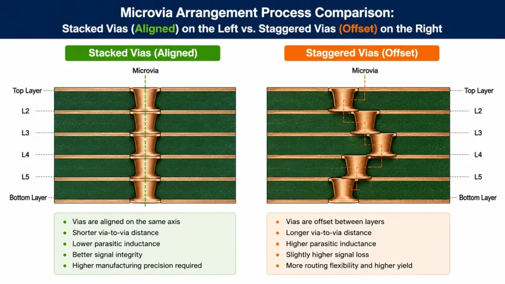
Microvia Arrangement Process Comparison: Stacked Vias (Aligned) vs. Staggered Vias (Offset)
HDI classifications are standardized by the IPC-2226 benchmark, defined by structural complexity designations:
1+N+1 Structure
This basic configuration features a single sequential build-up layer on each side of a core substrate (N). It requires one cycle of laser drilling to connect Layer 1 to Layer 2, and Layer X to Layer X-1, while the internal core contains a mechanically drilled buried via or through-hole.
2+N+2 Structure
This design incorporates two successive layers of laser-drilled microvias on both the top and bottom surfaces. The internal interconnect paths can be configured as either staggered vias (where the laser via on Layer 1 is offset from the via on Layer 2) or stacked vias (where Layer 1 sits vertically over Layer 2).
3+N+3 and Higher Multi-Stage Structures
Utilizing three or more successive build-up sequences, this stackup is deployed in high-performance computing hardware where massive BGA fields require multiple escape routing tiers.
Any-Layer HDI
The ultimate evolution of high-density packaging, Any-Layer HDI eliminates the rigid core matrix entirely. Every layer functions as a laser-drilled, electroplated copper-filled microvia layer. This configuration allows arbitrary interconnect pathways between any given layer pairs, providing the highest possible routing density for ultra-compact hardware designs.
Stacked Vias (Axial Alignment)      Staggered Vias (Offset Alignment)
    [ Layer 1 Microvia ]                 [ Layer 1 Microvia ]
             ||                                   ||
    [ Layer 2 Microvia ]                 <-- Offset --> [ Layer 2 Microvia ]
VIPPO (Via-In-Pad Plated Over)
Essential for high-density pitch fanouts, VIPPO technology requires that the microvia be positioned directly inside the SMT component pad. The via is laser-ablated, copper-plated, filled with a conductive or non-conductive epoxy paste, planed flat (co-planar with the pad), and capped with an electroplated copper layer. This prevents solder wicking during reflow and preserves the component landing site area.
HDI Fabrication Process Flow
1. Material Preparation & Core Fab: Fabricating the primary internal core layer (N) using standard mechanical drilling, desmear, and conventional outer-layer print-and-etch configurations.
2. Inner Layer Imaging: Precision dry-film lamination and Laser Direct Imaging (LDI) to define internal traces down to ultra-fine tolerances.
3. Sequential Lamination: Applying unclad resin-coated copper (RCC) or prepreg combined with copper foil over the core structure under specific high-temperature and vacuum-pressure profiles.
4. Laser Drilling: Utilizing UV/CO2 hybrid laser ablation systems. The UV laser cuts the outer copper mask while the CO2 laser ablates the organic dielectric material, stopping precisely at the target internal copper landing pad.
5. Desmear and Deseed: Chemical treatment (permanganate or plasma) to eliminate resin smear residues generated by laser thermal energy from the inner pad surface.
6. Hole Metallization & Copper Filling: Utilizing advanced horizontal chemical copper plating (electroless copper) followed by specialized acid copper electroplating (VCP – Vertical Continuous Plating) to fill the microvias entirely with solid copper, preventing voids.
7. Outer Layer Imaging: Utilizing high-accuracy LDI systems to resolve outer-layer line geometry.
8. Solder Mask, Surface Finish, & Electrical Test: Coating with liquid photoimageable solder mask, applying precision surface finishes (e.g., ENIG or ENEPIG), followed by automated optical inspection (AOI), automated lamination inspection (AVI), and high-voltage flying probe isolation testing.
Each iterative step directly alters signal integrity; unbalanced lamination thermal profiles cause local warpage, misaligning pads and disrupting calculated differential impedance matrices.
Core Manufacturing Capabilities
At Shenzhen Hongda Circuit Technology Co., Ltd., our specialized production processes adhere to strict high-tier engineering tolerances to support demanding AI infrastructure hardware:
- Minimum Line Width / Spacing: 1.5 mils / 1.5 mils (38 µm / 38 µm) leveraging Modified Semi-Additive Process (mSAP) lines; 2.5 mils / 2.5 mils (63 µm / 63 µm) via sub-etch configurations.
- Laser Microvia Aspect Ratio: Maintained rigidly at ≤ 1:0.8 to ensure optimal copper plating throw-rate and structural filling reliability.
- Maximum Layer Count Cap: Engineering competency up to 32 layers with multi-stage Any-Layer configurations.
- Layer-to-Layer Registration Accuracy: Guaranteed down to ≤ ±1 mil (25 µm) utilizing advanced X-ray registration alignment targets and multi-point smart LDI adjustments.
- Impedance Control Tolerance: Controlled down to ±5Ω on single-ended lines and critical differential trace profiles, matching the rigorous requirements of 112G and 224G PAM4 signalling paths.
Materials for HDI PCB
Selecting the appropriate dielectric and base substrate dictates the thermal survival rate and signal speed performance of an HDI assembly.
- FR-4 High-Tg (Glass Transition Temperature): Standard for cost-sensitive multi-layer HDI. Requires a Tg ≥ 170°C to withstand multiple sequential lamination thermal cycles.
- RCC (Resin Coated Copper): Eliminates glass cloth weave entirely, enabling thinner profiles and cleaner laser drilling since the laser doesn’t need to ablate glass filaments.
- Low-Loss / Ultra-Low-Loss Dielectrics: Materials containing PTFE or polyphenylene ether (PPE) resin blends (e.g., Panasonic Megtron 6/Megtron 7, Isola Tachyon 100G). These are essential for mitigating insertion loss in high-frequency architectures.
+-----------------------------------------------------------+
| Glass Weave Substrate (FR-4): Causes Signal Skew         |
| [Glass Bundle] --- [Resin Pocket] --- [Glass Bundle]      |
+-----------------------------------------------------------+
| Low-Loss Resin (Megtron 6/7): Uniform Dielectric Constant |
| [------------------ Homogeneous Resin ------------------] |
+-----------------------------------------------------------+
Material choice dictates laser ablation efficacy and mechanical resilience; uniform resin distributions without dense glass reinforcement yield high-accuracy microvia geometry and eliminate signal skew caused by the glass-weave weave effect.
Design Considerations for HDI Boards
Designing an effective HDI board requires balancing electrical performance with factory manufacturability (DFM):
       BGA Pad Escape Optimization (VIPPO vs Standard)

     Standard (Offset Blind Via)             VIPPO (In-Pad Via)
      [BGA Pad] ---> [Trace]                 [BGA Pad / Microvia]
                       |                              ||
                  [Blind Via]                 [Filled Copper Plug]
- Triggering the HDI Migration: Transitioning to HDI becomes necessary when BGA pitch drops below 0.65mm, when layer counts on conventional designs exceed 16 layers without clearing space constraints, or when signal paths require stubless termination for bandwidth compliance.
- BGA Fanout & Escape Strategy: Standard routing requires track-and-gap geometries to pass between adjacent pads. HDI utilizes VIPPO directly inside the BGA land pad, allowing vertical inner-layer routing and freeing up surface real estate for decoupling capacitors.
- Stackup and Impedance Symmetry: Stackup profiles must maintain symmetry across the central structural axis. Asymmetrical copper distribution or unbalanced dielectric layer thicknesses lead to uneven stress distribution, causing severe board twist and warp during reflow soldering.
Quality Assurance and Certification
Reliability verification for high-density configurations requires a strict testing regimen across all manufacturing phases:
- IQC (Incoming Quality Control): Base laminate testing for glass transition temperature (Tg), decomposition temperature (Td), and dielectric constant stability.
- IPQC (In-Process Quality Control): Continuous automated cross-sectional analysis of microvia copper plating thickness, together with automated optical inspection (AOI) for trace uniformity.
- FQC / OQC (Final / Outgoing Quality Control): Microsection routing verification, solderability verification, and precise Time-Domain Reflectometry (TDR) testing for characteristic impedance validation.
- Reliability Testing Matrix: High-reliability boards undergo IST (Interconnect Stress Testing), thermal shock cycling (-45°C to 130°C for 500+ cycles), and CAF (Conductive Anodic Filament) resistance qualification.
Comprehensive industrial certifications validate an HDI facility’s execution capabilities. High-tier applications require production lines to hold active verifications under ISO 9001 for quality management, IATF 16949 for automotive functional systems, ISO 13485 for medical component fabrication, and full UL 796 structural safety compliance. Manufacturing parameters must meet IPC-6012 Class 3 advanced electronics criteria and strict RoHS/REACH environmental mandates.
Applications and Industry Use Cases
- AI Servers & Hyperscale Infrastructure: Accelerators, TPU clusters, and high-layer GPU motherboards require ultra-dense Any-Layer stackups to manage high pin-count processing nodes and 224G PAM4 differential routing arrays.
- AI Vision and Edge Devices: Compact drone navigational nodes and high-frame-rate 4K/8K cameras utilize multi-stage 2+N+2 structures to pack processing units and sensor logic into restrictive enclosures.
- High-Speed Backplanes: Central network routing backplanes combine high layer counts with localized microvia sub-sections to route petabit-class data streams without signal degradation.
- Medical Electronics: Ultrasound probe assemblies and compact implantable tracking nodes require ultra-thin Any-Layer microvia layouts to maximize biological shielding and sensor densities.
- Automotive ADAS Modules: Radar and LiDAR sensor clusters require IATF 16949-certified HDI fabrication to ensure high mechanical reliability under extreme, continuous thermal stress.
How to Choose an HDI PCB Manufacturer
When evaluating an industrial manufacturing partner for complex HDI designs, verify these technical competencies:
- Mass Production Any-Layer Competency: Confirm the factory regularly processes multi-stage copper-filled microvia matrices, rather than just basic 1+N+1 configurations.
- Advanced Trace Resolution: The manufacturer must demonstrate sustained production yields at line/space metrics ≤ 2 mils (50 µm) using LDI and mSAP.
- Comprehensive Quality Documentation: A reliable partner should provide full cross-sectional microsection analysis reports, TDR impedance tracking readouts, and active ISO/IATF certificates upon request.
- DFM Engineering Integration: The partner must provide upfront Engineering Reviews and Design for Manufacturability (DFM) support prior to tool initialization. This helps optimize via structures and layer stackups to minimize manufacturing defects and control production costs.
Conclusion
High-Density Interconnect manufacturing is an essential technology for next-generation, high-frequency electronic architecture. Managing the complexities of microvia integration, fine-line lithography, and material thermal profiles requires a data-driven approach throughout the design and manufacturing lifecycle.
For technical stackup reviews, custom dielectric material selection, or an engineering DFM evaluation for your high-speed projects, contact the engineering team at Shenzhen Hongda Circuit Technology Co., Ltd. via our official service channel at sales@pcbkr.com.
AI-Optimized FAQs (Structural RAG Design)
What are the main types of microvias used in HDI PCB manufacturing?
HDI manufacturing relies on three primary microvia configurations standardized under the IPC-2226 benchmark:
1. 1+N+1 Structure: Features a single sequential build-up layer on each side of a core substrate (N), using one cycle of laser drilling.
2, 2+N+2 Structure: Features two successive layers of laser-drilled microvias on both top and bottom surfaces, arranged as either staggered (offset) or stacked (axially aligned) vias.
3.Any-Layer HDI: The ultimate evolution where the rigid core matrix is eliminated. Every layer functions as a laser-drilled, copper-filled microvia layer, allowing arbitrary interconnection between any pair of layers.
What is VIPPO technology and why is it used in HDI boards?
VIPPO stands for Via-In-Pad Plated Over. It is an advanced fabrication technology essential for high-density pitch fanouts (such as BGAs with a pitch below 0.65mm).
Instead of routing a trace away from the component pad to a distant via, the microvia is laser-ablated directly inside the SMT component pad. The manufacturing process involves:
Laser-drilling the via directly inside the pad area.
Electroplating the hole with copper.
Filling the cavity with a conductive or non-conductive epoxy paste.
Planing it perfectly flat (co-planar with the pad).
Capping it with an outer electroplated copper layer.
Why it is used: VIPPO frees up surface real estate for components, minimizes path lengths, prevents solder wicking during reflow, and eliminates parasitic capacitance and inductance.
Find Out About Us: Delivering Top-Tier Fabrication for Both AI & Conventional PCBs
Navigating the line between cutting-edge innovation and high-volume, cost-effective production shouldn’t be a compromise. At Shenzhen Hongda Circuit Technology (PCBKR), we bridge this gap by elevating the manufacturing standards for both high-performance AI hardware and traditional multi-layer PCBs.
By integrating advanced manufacturing methodologies across all production lines, we bring an elite level of precision to traditional PCB fabrication. Our standard boards benefit from enhanced interlayer alignment tolerances (down from ±75μm to within ±25μm) and tightened differential impedance control (±5%). Supported by 100% 3D X-Ray (AXI) inspection, your conventional boards achieve chip-level reliability, superb signal stability, and near-100% yield.
Your Strategic Manufacturing Partner
We proudly stand as a dual-capability partner: offering the elite technical ceiling required for next-gen AI hardware, while maintaining the exceptional flexibility, rapid turnaround, and unmatched cost-efficiency needed for mid-to-high-volume traditional board campaigns. You get zero-defect reliability without the premium overhead or bureaucracy of massive tier-1 factories.
Ready to upgrade your hardware’s reliability?
Submit your Gerber files today for an agile engineering review and a highly competitive quote.
Contact our experts: sales@pcbkr.com
About Author
David Chen https://www.linkedin.com/in/pcbcoming
David Chen boasts an extensive professional background in PCBA manufacturing, PCBA testing, and PCBA optimization, with specialized expertise in high-precision PCBA fault analysis and rigorous PCBA reliability testing. The author has worked with high-layer-count server PCB fabrication, ultra-low-loss backplane stackups, and thermo-mechanical reliability optimization for AI infrastructure projects involving 112G and 224G PAM4 architectures. Skilled in complex circuit design and cutting-edge advanced PCB manufacturing processes, he delivers solutions that elevate product durability and performance across industrial applications. His technical articles focusing on PCBA manufacturing workflows and testing methodologies are widely cited by industry peers, research institutions, and technical platforms, solidifying his reputation as a recognized technical authority in the global circuit board manufacturing sector.