How to Optimize HDI PCB Costs at the Design Stage
A Technical & Procurement Guide by Shenzhen Hongda Circuit Technology Co., Ltd.
Updated for 2026 PCB Manufacturing Technology
Introduction: Why HDI Costs Must Be Controlled at the Design Stage
HDI (High-Density Interconnect) PCBs are at the heart of today’s most advanced electronics — from 5G smartphones and AI edge devices to advanced automotive ADAS modules and medical wearables. Yet one of the most persistent misconceptions in the industry is that HDI cost is driven primarily by a single process step. In reality, HDI cost is a compound result of multiple interacting factors: microvia count and laser drilling cycles, sequential lamination passes, material selection, copper thickness, impedance requirements, and manufacturing yield.
At Shenzhen Hongda Circuit Technology Co., Ltd., we have been manufacturing HDI PCBs for global customers since our founding, and we have observed one consistent truth: the earlier your design team engages with cost optimization principles, the more effectively unnecessary high-order HDI structures and expensive process steps can be avoided — without sacrificing board performance.
This guide is written for both PCB design engineers and procurement professionals. Engineers will find actionable design rules that reduce cost at the source. Procurement teams will find frameworks for evaluating supplier quotes and asking the right questions. Together, these perspectives form a complete approach to HDI cost management in 2026.
The Main Cost Drivers of HDI PCBs
1.Microvias and Laser Drilling Cycles
Microvias — typically < 150 µm in diameter — are the defining feature of HDI boards, enabling higher component density and shorter signal paths. However, each laser drilling cycle adds significant cost. The laser drill machine time, the need for precise depth control, and the higher probability of drill defects (misregistration, insufficient copper fill, void formation) all accumulate into meaningful cost per cycle.
A practical rule of thumb used in modern 2026 HDI fabrication: reducing the number of laser drilling passes has a greater impact on cost than incremental improvements to any individual process parameter. If your design requires three laser passes to accommodate a 3+N+3 structure, switching to a 1+N+1 structure — where technically permissible — can reduce laser-related costs by 50% or more.
The 2026 manufacturing landscape also sees increasing adoption of UV-CO2 combined laser systems that can drill copper-clad microvias in a single pass, reducing cycle time. However, these systems require tighter pad size and annular ring tolerances, meaning the design must be optimized to take advantage of them.
2.Sequential Lamination Passes
Sequential lamination — pressing multiple sub-constructions together in successive cycles — is the most process-intensive aspect of HDI manufacturing. Each lamination pass introduces a full manufacturing cycle: lay-up, pressing, cooling, inspection, drilling, plating, etching, and outer layer processing.
A useful way to frame this for engineers and procurement alike: every additional lamination pass adds one more complete manufacturing cycle — and with it, one more opportunity for dimensional distortion, misregistration, and yield loss. A 2+N+2 HDI structure requires two lamination passes before the core; a 3+N+3 requires three. Each step increases lead time, process complexity, and total board cost.
In 2026, leading-edge PCB manufacturers including Hongda are increasingly offering Any-Layer HDI (ALHDI) capabilities, where every layer can contain microvias. While ALHDI offers maximum routing density, it also involves the highest number of sequential lamination passes and should only be specified when truly necessary for signal density or package integration requirements.
3.Layer Count, Board Thickness, and Material Selection
Layer count is not the only cost driver in HDI boards — material selection, copper weight, and controlled impedance requirements all interact with layer count to determine final cost. A 10-layer board built on Rogers 4350B with 1 oz copper on all signal layers will cost significantly more than the same layer count on Isola FR408HR with 0.5 oz copper on inner layers.
The 2026 material landscape offers several cost-optimized options for HDI applications. Low-loss laminates such as Panasonic Megtron 6 and Isola I-Tera MT40 provide excellent high-frequency performance at a lower cost premium than traditional PTFE-based materials. For designs that do not require extreme loss performance, these materials offer a compelling balance of electrical performance and manufacturability.
A key reminder for design teams: not every design requires the highest-order HDI structure available. A carefully optimized 4-layer HDI board with 1+N+1 structure often outperforms a poorly planned 8-layer conventional board in both density and cost. Matching the HDI order to actual routing requirements — rather than defaulting to a higher order for safety margin — is one of the most impactful cost decisions available to a design team.
Cost Reduction Through Via Structure Optimization
1.Stacked Vias vs. Staggered Vias
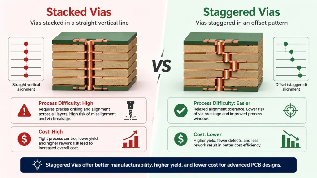
Cross-section comparison showing why staggered vias offer better manufacturability, higher yield, and lower fabrication costs compared to stacked vias.
Stacked microvias (where a via on one layer is directly above a via on the layer below, sharing a common pad) are generally more expensive than staggered microvias (where vias on adjacent layers are offset from each other). The reason is process-related: stacked vias require very precise copper filling of the lower via before drilling the upper via, with tight tolerance requirements on fill height, surface planarity, and copper grain structure.
The practical design guideline: if your electrical constraints and routing density allow it, evaluate staggered via structures first. Reserve stacked vias for areas where routing density truly demands them — typically under fine-pitch BGA components with tight escape routing requirements. In 2026, even advanced chip packages at 0.4 mm pitch can often be escaped with staggered vias on a well-planned stackup.
2.Reducing Unnecessary Blind and Buried Vias
It is common for design teams, particularly on complex boards, to apply blind or buried vias broadly across a design as a conservative measure — ensuring routing flexibility in all regions. However, this approach significantly increases cost. Each blind/buried via pair adds process steps that are only needed where they are actually used.
A cost-effective approach: restrict blind and buried vias to regions where through-hole vias are genuinely insufficient due to component density or signal integrity constraints. In non-critical routing areas, return to conventional through-hole vias or standard dogleg routing. This targeted approach can reduce the active HDI area — and its associated costs — to a fraction of the total board.
3.Using Microvias Only Where Required
Localized HDI is one of the most powerful cost reduction strategies available. Rather than specifying HDI processes across the entire board, confine HDI microvia regions to areas immediately surrounding high-density components (BGAs, advanced FPGAs, SoC packages). The rest of the board can be manufactured using standard through-hole vias and conventional processes.
This approach — sometimes called embedded or island HDI — is well-supported by 2026 manufacturing capabilities. At Shenzhen Hongda Circuit Technology, we routinely produce boards where HDI zones cover as little as 15-20% of the total board area, with the remainder manufactured at standard process costs. The result is a board that meets all density requirements at significantly lower total cost.
Optimize HDI PCB Cost Reduction Through HDI Order Strategy
1.Prioritizing Lower-Order HDI Structures
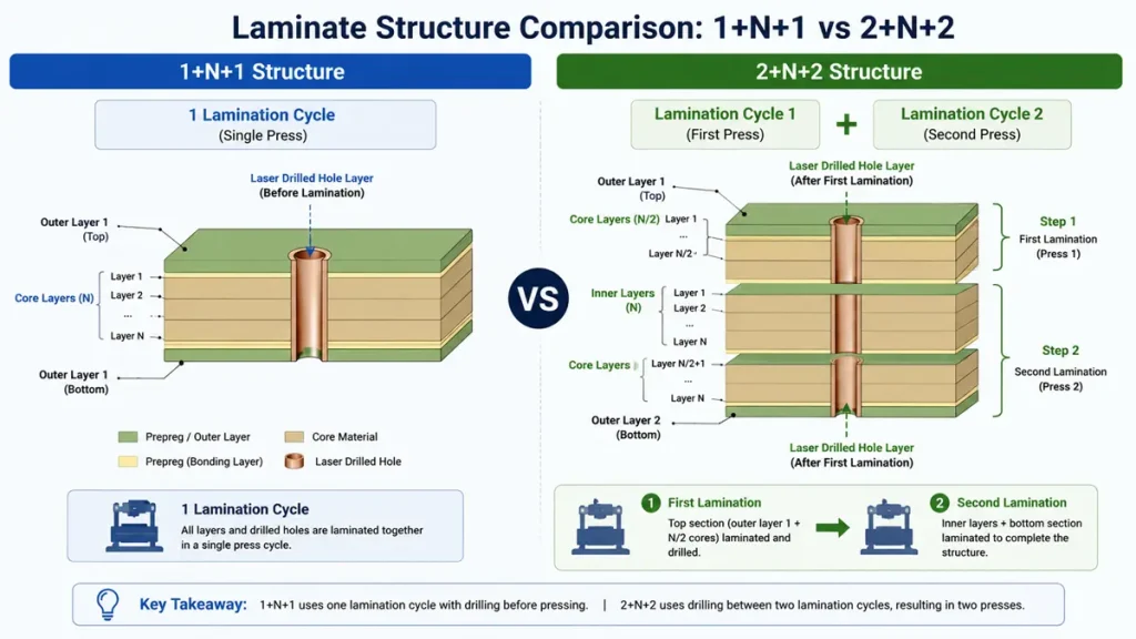
Stackup and process comparison demonstrating how a 1+N+1 structure consolidates production into a single lamination cycle, whereas a 2+N+2 structure forces multiple sequential presses and independent drilling stages.
The HDI order — 1+N+1, 2+N+2, 3+N+3, Any-Layer — directly determines manufacturing cost and lead time. A 1+N+1 structure, with a single microvia layer on each side of the core, requires only one lamination pass per side and one laser drilling cycle. A 2+N+2 structure doubles this to two passes and two drilling cycles per side.
For procurement teams: as a general rule, each step up in HDI order increases both cost and lead-time risk. A 2+N+2 structure typically costs 40-80% more than an equivalent 1+N+1 design, and lead time increases proportionally. When evaluating design decisions from a procurement perspective, any step toward lower-order HDI is a direct reduction in both cost and supply chain risk.
In 2026, leading HDI manufacturers have significantly improved yield on 1+N+1 structures through advances in laser parameter control and copper plating uniformity. This makes 1+N+1 an even more attractive default choice for designs that previously might have required 2+N+2 as a yield safety measure.
2.Consolidating Structures to Reduce Build Cycles
Design teams should review whether multiple localized HDI requirements across a board can be consolidated into a fewer-layer process flow. For example, a design with separate 1+N+1 regions on multiple areas might be consolidatable into a single uniform build that still meets density requirements while eliminating the complexity of multiple transition zones.
A practical approach: audit each blind/buried via pair for whether it could be replaced by an optimized through-via with appropriate anti-pad clearances. In many designs, 20-30% of blind/buried vias can be replaced without functional impact, reducing the active HDI process area and its associated cost.
Cost Reduction Through Design-Level Decisions
1.Reducing Laser Layer Count
The number of layers that require laser drilling is one of the primary cost multipliers in HDI manufacturing. Each laser-drilled layer requires its own drilling setup, laser parameter calibration, depth inspection, and plating cycle. Reducing the number of laser-drilled layers — even by one — can produce meaningful cost savings.
Key design principle for 2026: when routing constraints allow, favor stackup configurations that minimize the number of laser-drilled layers. For example, a design that places all microvias on two outer layers (L1-L2 and L(n-1)-Ln) can often be manufactured with fewer laser passes than a design that distributes microvias across interior layer pairs. Working with your fabricator early in the design process to evaluate stackup alternatives is one of the highest-ROI activities in HDI cost optimization.
2.Optimizing Via Diameter, Spacing, and Density
Via diameter and spacing directly affect yield, drill throughput, and plating uniformity. Pushing vias to the smallest diameter and tightest spacing that a design tool allows — without consulting with the fabricator — is a common source of unnecessary cost. Overly tight via density increases laser drilling time, reduces plating bath efficiency, and narrows the process window, all of which reduce yield and increase cost.
The 2026 industry standard for cost-optimized HDI microvias is a finished hole diameter of 100 µm with a 200 µm pad — achievable with high reliability using current UV laser systems. Going below 75 µm finished hole diameter significantly increases process cost and should only be done when absolutely required by component pitch or routing density. Giving your fabricator a stable, manufacturable process window by avoiding extreme via miniaturization is directly rewarded in yield and cost.
Cost Reduction Through Lamination and Structure Simplification
1.Reducing Lamination Pass Count
As discussed in Section 2.2, each lamination pass is effectively a complete sub-manufacturing cycle. Reducing lamination passes is one of the most impactful structural decisions available at the design stage. A standard question in any HDI design review should be: can this design achieve its density requirements with fewer lamination passes?
In 2026, process improvements in laser drilling depth control and plating uniformity have made it feasible to achieve routing densities that previously required 2+N+2 structures using optimized 1+N+1 designs. The key is working closely with your fabricator to explore stackup alternatives before finalizing the design. At Shenzhen Hongda Circuit Technology, our engineering team regularly collaborates with customers during the design phase to identify lamination-reducing alternatives without compromising electrical performance.
2.Avoiding Whole-Board Upgrades for Local Requirements
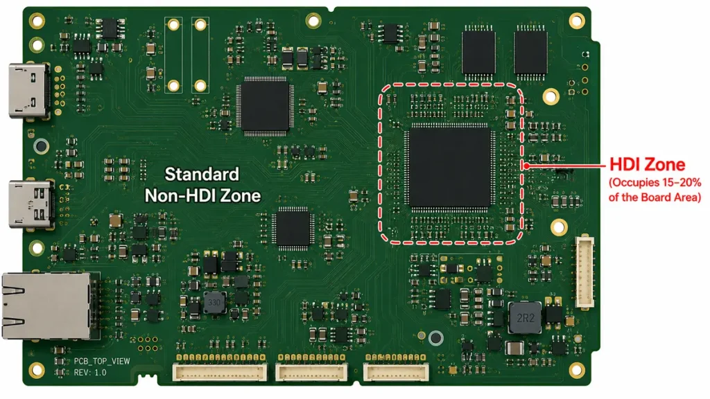
Top-view example of Localized (Island) HDI design. Sourcing costs are dramatically reduced by confining premium high-order structures to the 15-20% area surrounding the dense BGA chip, while the remaining 80% utilizes standard cost-efficient processes
One of the most common and avoidable HDI cost escalations occurs when a design team upgrades the entire board to a higher HDI order because of local density requirements in a small area — typically the escape routing zone of a single high-density BGA. The result is a board where 90% of the area is manufactured at a higher process tier than necessary.
The 2026 solution: localized or hybrid HDI. Confine high-order HDI structures to the specific area where they are needed, and design the rest of the board with a lower-order structure or conventional processes. This approach requires slightly more careful stackup planning and design rule management at the transition zones, but the cost savings are substantial — often 25-40% reduction in total board cost for designs with one or two dense component areas surrounded by less dense regions.
Engineering and Procurement Checklist
1.Design Engineer Review Checklist
Before finalizing an HDI PCB design for fabrication, engineers should review the following:
- Are stacked vias truly required, or can staggered vias meet the same electrical and density requirements?
- Can the number of laser drilling layers be reduced by one or more through stackup reorganization?
- Are blind and buried vias restricted to areas where through-hole vias are genuinely insufficient?
- Can the HDI order be reduced from 2+N+2 to 1+N+1 without compromising routing density?
- Is HDI applied locally to high-density component areas, or unnecessarily extended across the entire board?
- Are via diameters and spacings within the fabricator’s cost-optimized process window (e.g., 100 µm finished hole, 200 µm pad)?
- Has the lamination pass count been minimized, with design review confirming no redundant build cycles?
- Has the design team consulted with the fabricator (e.g., Shenzhen Hongda) on stackup optimization before design freeze?
3.Procurement Team Verification Checklist
When sourcing HDI PCBs, procurement professionals should confirm the following with potential suppliers:
- Request a comparison quote for the specified HDI structure AND at least one lower-order alternative (e.g., quote both 2+N+2 and optimized 1+N+1 if applicable).
- Clarify how laser drilling is priced — is it per pass, per layer, or per hole? Understanding the billing model allows direct comparison of structural alternatives.
- Confirm how sequential lamination passes are priced — are they included in a fixed-price model or billed incrementally?
- Ask whether yield risk is priced into the per-unit cost or handled separately as a scrap provision. This is particularly important for complex HDI structures.
- Request DFM (Design for Manufacturability) feedback from the fabricator before placing the order — reputable HDI manufacturers will identify cost-reduction opportunities proactively.
- Confirm that the supplier has 2026-current laser drilling capabilities (UV-CO2 combined systems, automated depth control) to ensure the design is manufacturable at competitive yield levels.
2026 Technology Highlights in HDI PCB Manufacturing
The HDI PCB manufacturing landscape has advanced significantly in 2026. Shenzhen Hongda Circuit Technology has integrated the following current-generation capabilities that directly benefit cost-optimized HDI designs:
- UV-CO2 Combined Laser Drilling: Single-pass drilling of copper-clad microvias down to 75 µm diameter, reducing laser cycle time and enabling tighter pad geometries.
- Advanced Copper Filling (Type VI Fill): Full copper fill of microvias with < 5 µm surface dimple, enabling reliable stacked via structures with reduced annular ring requirements.
- AI-Assisted Stackup Optimization: Machine learning models trained on yield data from thousands of HDI designs are used to evaluate stackup alternatives and predict yield impact before manufacturing.
- Any-Layer HDI (ALHDI) Production Capability: Full production capability for any-layer HDI with up to 16 layers, with automated AOI inspection at each lamination stage.
- Low-Loss Material Portfolio: Qualified supply chain for Panasonic Megtron 6, Isola I-Tera MT40, Rogers 4350B, and Ventec VT-901, enabling material selection optimization across price-performance tradeoffs.
- Real-Time Yield Monitoring: SPC (Statistical Process Control) integrated into all critical process steps, providing live yield data that supports continuous improvement and competitive pricing on repeat orders.
FAQ: Questions Frequently Asked by PCB Buyers and Procurement Engineers
What is the price difference between 1+N+1 and 2+N+2 HDI PCB structures, and when should I choose the lower-order option?
A 2+N+2 HDI PCB typically costs 40–80% more than an equivalent 1+N+1 design, with lead time increasing by 30–50% due to the additional lamination and laser drilling cycles. You should consider 1+N+1 whenever your routing density requirements can be met with a single microvia layer on each side of the core — which is possible for most designs using components with ≥ 0.5 mm BGA pitch. At Shenzhen Hongda Circuit Technology, our engineering team provides free stackup analysis to help you determine whether a lower-order structure is feasible for your specific design. In 2026, process improvements have made it possible to achieve routing densities on 1+N+1 boards that previously required 2+N+2, making the cost trade-off even more favorable for lower-order designs.
How does the number of laser drilling passes affect my HDI PCB quote, and what can I do in the design to reduce it?
Laser drilling is one of the most significant cost drivers in HDI fabrication. Each drilling pass involves machine setup, parameter calibration, depth inspection, and dedicated plating cycles. Reducing laser passes from three to two — or two to one — can reduce HDI-related manufacturing costs by 30–50%. Design-level actions that reduce laser passes include: choosing lower-order HDI structures (1+N+1 vs. 2+N+2), confining microvias to fewer layer interfaces, using staggered rather than stacked vias where possible, and collaborating with your fabricator on stackup alternatives before design freeze. When requesting a quote from Shenzhen Hongda Circuit Technology, ask for a “laser pass comparison” — we will show you the cost impact of alternative drilling configurations for your specific design.
What is the minimum order quantity (MOQ) for HDI PCBs, and how does prototype pricing compare to production pricing?
At Shenzhen Hongda Circuit Technology, we support HDI PCB orders from prototype quantities (as few as 5 panels) through full production volumes (tens of thousands of boards per month). Prototype pricing for HDI boards typically carries a 2–4x cost premium over production pricing due to setup amortization, engineering review, and process qualification costs that are spread over fewer units. For recurring designs, we offer a structured NPI-to-production transition that locks in production pricing once the design has been qualified at prototype stage. We recommend that procurement teams factor this transition into their sourcing strategy: a slightly higher prototype cost is fully offset by optimized production pricing once volume ramps. Contact our sales team for a specific prototype vs. production cost comparison for your HDI design.
How do I evaluate an HDI PCB supplier’s quality and reliability before placing a first order?
Evaluating an HDI PCB supplier requires looking beyond the initial price quote. Key criteria for 2026 include: ISO 9001 and IATF 16949 certification (for automotive-grade HDI), IPC Class 2 or Class 3 manufacturing capability, documented microvia fill qualification data (including cross-section images showing copper fill quality), SPC data from critical process steps, and references from customers in your industry segment. Shenzhen Hongda Circuit Technology provides prospective customers with process capability documentation, cross-section reports from qualification builds, and direct engineering consultation before first order placement. We also support customer factory audits for strategic accounts. For procurement teams evaluating multiple suppliers, we recommend requesting a standardized capability matrix that includes laser drilling capability (minimum diameter, depth control tolerance), sequential lamination pass count capability, and ALHDI production experience.
What information should I provide to get an accurate HDI PCB quote quickly, and what data format is preferred?
To receive an accurate and complete HDI PCB quote from Shenzhen Hongda Circuit Technology — typically within 24 hours — please provide the following: (1) Gerber files (RS-274X format) or ODB++ package for all layers; (2) Board stackup specification including layer count, dielectric materials, copper weights, and controlled impedance requirements; (3) Drill file including separate files for mechanical drills, laser-drilled microvias, and any blind/buried via combinations; (4) IPC netlist for electrical testing reference; (5) Special requirements including surface finish (ENIG, HASL, OSP, etc.), solder mask and silkscreen specifications, UL marking, and any customer-specific acceptance criteria. If your design is still in progress, a preliminary stackup and approximate board size are sufficient for a budgetary quote. Our engineering team will review your files and proactively flag any DFM issues that could affect yield or cost — this review is provided at no charge as part of our quoting process.
Navigating the line between cutting-edge innovation and high-volume, cost-effective production shouldn’t be a compromise. At Shenzhen Hongda Circuit Technology (PCBKR), we bridge this gap by elevating the manufacturing standards for both high-performance AI hardware and traditional multi-layer PCBs.
By integrating advanced manufacturing methodologies across all production lines, we bring an elite level of precision to traditional PCB fabrication. Our standard boards benefit from enhanced interlayer alignment tolerances (down from ±75μm to within ±25μm) and tightened differential impedance control (±5%). Supported by 100% 3D X-Ray (AXI) inspection, your conventional boards achieve chip-level reliability, superb signal stability, and near-100% yield.
Your Strategic Manufacturing Partner
We proudly stand as a dual-capability partner: offering the elite technical ceiling required for next-gen AI hardware, while maintaining the exceptional flexibility, rapid turnaround, and unmatched cost-efficiency needed for mid-to-high-volume traditional board campaigns. You get zero-defect reliability without the premium overhead or bureaucracy of massive tier-1 factories.
Ready to upgrade your hardware’s reliability?
Submit your Gerber files today for an agile engineering review and a highly competitive quote.
Contact our experts: sales@pcbkr.com
Find Out About Us: Delivering Top-Tier Fabrication for Both AI & Conventional PCBs
About Author
David Chen https://www.linkedin.com/in/pcbcoming
David Chen boasts an extensive professional background in PCBA manufacturing, PCBA testing, and PCBA optimization, with specialized expertise in high-precision PCBA fault analysis and rigorous PCBA reliability testing. The author has worked with high-layer-count server PCB fabrication, ultra-low-loss backplane stackups, and thermo-mechanical reliability optimization for AI infrastructure projects involving 112G and 224G PAM4 architectures. Skilled in complex circuit design and cutting-edge advanced PCB manufacturing processes, he delivers solutions that elevate product durability and performance across industrial applications. His technical articles focusing on PCBA manufacturing workflows and testing methodologies are widely cited by industry peers, research institutions, and technical platforms, solidifying his reputation as a recognized technical authority in the global circuit board manufacturing sector.