5G Antenna PCB, Radar High Frequency PCB, and Microwave PCB Assembly
Introduction: Why High Frequency PCB Design Has Reached a Turning Point in 2026
The proliferation of 5G networks, automotive ADAS systems, and next-generation satellite communication has placed extraordinary pressure on PCB manufacturers to deliver boards that perform reliably at gigahertz and millimeter-wave frequencies. Standard FR-4 laminates—adequate for most consumer electronics—cannot maintain acceptable signal integrity above roughly 1 GHz. The result is a sharp industry pivot toward specialized high frequency PCB fabrication, where dielectric loss, impedance control, and surface roughness are no longer secondary concerns but primary design constraints.
At Shenzhen Hongda Circuit Technology Co., Ltd., we have tracked this transition closely. Over the past two years, 5G antenna PCB orders have grown more than 60% year-over-year, requests for 77 GHz automotive radar high frequency PCB production have tripled, and demand for turnkey microwave PCB assembly services—covering everything from PTFE laminate sourcing to precision SMT—has expanded into new verticals including drone payloads and fixed satellite ground stations.
This article provides an engineer-level walkthrough of the three most technically demanding product categories we manufacture, the 2026 advances that are reshaping process tolerances and material choices, and the practical decisions every design and procurement team must confront before placing a production order.
The Physics Driving 5G Antenna PCB Complexity
A 5G antenna PCB does not merely carry signals—it shapes them. At sub-6 GHz, radiation efficiency and impedance matching dominate; at mmWave frequencies (24 GHz to 100 GHz), every millimeter of trace geometry, every via transition, and every laminate surface imperfection becomes a loss mechanism. Engineers who treat mmWave antenna substrate selection as an afterthought discover this quickly during first-article testing.
Sub-6 GHz versus mmWave 5G Antenna PCB: Different Problems, Different Materials
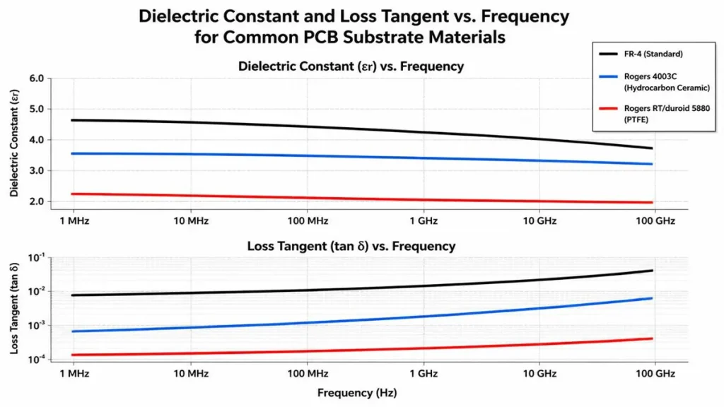
Dielectric Constant and Loss Tangent vs Frequency for PCB Substrates
Sub-6 GHz 5G antenna PCBs operate in a regime where Rogers 4003C or Taconic TLY-5 hydrocarbon ceramic laminates offer a workable balance of cost and performance. Dielectric constant (Dk) of 3.38–3.55 with loss tangent (Df) below 0.0027 at 10 GHz is sufficient to achieve acceptable gain on patch and slot antenna arrays feeding gNodeB radios.
mmWave 5G antenna PCB design is a different discipline entirely. Phased array modules operating at 28 GHz, 39 GHz, or 60 GHz demand PTFE-based laminates such as Rogers RT/duroid 5880 (Dk 2.20, Df 0.0009 at 10 GHz) or Rogers 3003 (Dk 3.00, Df 0.0010). Even at these loss figures, a 100 mm microstrip feed line at 28 GHz introduces measurable insertion loss; antenna-in-package (AiP) architectures are increasingly preferred precisely because they minimize inter-element trace lengths.
Massive MIMO and Phased Array Antenna PCB Stack-Up Architecture
Massive MIMO antenna PCB designs for 5G base stations typically require 8 to 16 layer stack-ups. Signal layers alternate with reference planes to control characteristic impedance, while blind and buried vias reduce the vertical transition stub length that would otherwise radiate spurious energy. In 2026, back-drilling—selectively removing via barrel stubs with a controlled-depth drill—has become standard practice at Hongda for any 5G antenna PCB layer count above eight, eliminating stubs that would resonate at frequencies harmonic to the operating band.
Isolation between antenna elements in a phased array PCB is equally critical. Mutual coupling degrades beam-steering accuracy. Guard traces, substrate-integrated waveguide (SIW) partitions, and localized ground stitching vias are all valid mitigation strategies, but each adds manufacturing complexity. Our DFM review process flags isolation gaps below the substrate-specific threshold before a single panel reaches the drilling floor.
Surface Finish Selection for 5G Antenna PCB Manufacturing
Immersion silver (ImAg) has gained significant traction for mmWave 5G antenna PCB production in 2026. Its surface roughness is lower than ENIG, which matters because skin depth at 28 GHz is approximately 0.5 µm—well within the roughness range of electroless nickel deposits. ENEPIG (Electroless Nickel Electroless Palladium Immersion Gold) remains the premium choice for designs that also carry fine-pitch BGAs or flip-chip components requiring wire-bondable pads. Hongda maintains all four primary high-frequency finishes in active production: ImAg, ENIG, ENEPIG, and OSP, with TDR-validated impedance test coupons on every panel.
Radar High Frequency PCB Manufacturing: Automotive, Defense, and Industrial Applications
Radar systems now appear in consumer automobiles, industrial forklifts, airport security scanners, and military platforms. What unifies them is an unforgiving electrical performance envelope: phase noise, insertion loss, and channel-to-channel amplitude imbalance must be held within tight tolerances across temperature extremes. Radar high frequency PCB fabrication is therefore one of the most process-intensive segments of the PCB industry.
77 GHz Automotive Radar PCB: The 2026 Production Standard
Automotive radar for ADAS applications has consolidated around 77 GHz (76–81 GHz band) with a growing transition to 79 GHz for higher-resolution short-range sensing. At these frequencies, the PCB substrate is no longer a passive carrier—its Dk, Df, and thermal coefficient of dielectric constant (TCDk) directly determine whether the antenna beam points where the system thinks it does across a –40°C to +125°C operating range.
Rogers RO3003G2 (Dk 3.00 ±0.04, Df 0.0010 at 77 GHz) and Rogers RO3003 have emerged as the dominant laminate choices for 77 GHz automotive radar high frequency PCB production. Taconic RF-60A and Isola Astra MT77 are qualified alternatives. Hongda’s automotive radar PCB line runs controlled impedance to ±5% tolerance with TDR verification on 100% of panels—tighter than the ±10% tolerance common in mainstream PCB fabrication.
Phase Consistency and Crosstalk Control in Radar High Frequency PCB Arrays
Multi-channel radar transceivers require that every RF trace feeding an antenna element carries identical electrical length—not just physical length. Propagation velocity depends on the local Dk of the surrounding laminate, which varies with fiber weave pattern, copper roughness, and laminate thickness uniformity. Trace length matching to 0.1 mm physical tolerance is insufficient when laminate Dk varies ±2% across a panel. Hongda compensates through pre-production dielectric constant sampling and trace length trimming against measured Dk values for high-channel-count radar high frequency PCB projects.
Crosstalk between adjacent RF channels in a multi-beam radar high frequency PCB is suppressed through a combination of ground-plane separation, microstrip-to-stripline transitions at crossing points, and edge-plated copper barriers between transmit and receive sections. The 2026 trend toward single-chip radar ICs driving 16 or more simultaneous antenna elements has made these layout disciplines non-optional.
HDI Radar High Frequency PCB: Laser Vias and Sequential Lamination
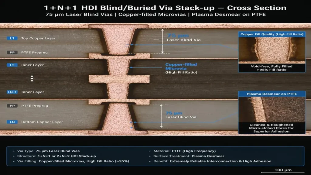
1+N+1 HDI Blind and Buried Via Cross Section
High-density interconnect (HDI) techniques are increasingly applied to radar high frequency PCB designs where the RF front-end IC pitch demands microvias that mechanical drills cannot produce. CO2 laser drilling creates microvias down to 75 µm diameter in PTFE-ceramic composites, though PTFE’s low surface energy requires plasma desmear before copper plating to achieve reliable via reliability. Hongda introduced a dedicated laser-via line for PTFE radar PCB substrates in late 2025, enabling 1+N+1 and 2+N+2 build-up structures on materials that previously required through-hole construction.
Microwave PCB Assembly: Precision PCBA for RF and Microwave Systems
Fabricating a high frequency PCB substrate to specification is half the battle. The second half is assembling RF and microwave components onto that substrate without degrading its electrical characteristics. Microwave PCB assembly demands SMT process parameters, solder volumes, and cleaning protocols that differ materially from standard FR-4 PCBA production.
SMT Process Control for Microwave PCB Assembly
QFN, BGA, and flip-chip RF components dominate modern microwave PCB assembly. QFN packages—common for RF power amplifiers and transceivers—require precise solder paste volume control because excess solder wicks beneath the exposed pad and alters the effective ground inductance. Hongda’s microwave PCBA line uses laser-cut stainless steel stencils at 0.10–0.12 mm thickness for RF footprints, with step-down apertures at chip capacitor pads to prevent bridging on 0201 components placed adjacent to RF transmission lines.
Reflow profile management is equally important. PTFE-based high frequency PCB laminates have a lower glass transition temperature than FR-4. A standard lead-free reflow profile peaking at 255°C can introduce micro-delamination at Rogers or Taconic laminate boundaries if ramp rates exceed 3°C/second. Hongda programs substrate-specific reflow profiles referenced against each laminate manufacturer’s thermal resistance data sheet.
RF Connector Integration in Microwave PCB Assembly
SMA, SMP, and end-launch GPO connectors are routinely assembled on microwave PCBs. Connector launch geometry—the physical transition from connector pin to PCB transmission line—is itself a microwave design problem. Improper launch design creates a reflection at the board edge that shows up as return loss degradation (S11 above –15 dB) and insertion loss spikes at specific frequencies. Hongda’s microwave PCBA process includes S-parameter measurement at the panel stage and post-assembly connector verification using a VNA calibrated to the specific connector series.
Shielding Enclosure Assembly for Microwave PCB PCBA
Many microwave PCB assembly orders include shielding enclosures—stamped or machined metal cans that enclose specific circuit sections to prevent spurious radiation or external interference. Proper enclosure assembly requires that seam gaps remain below λ/20 at the highest operating frequency. A 10 GHz design requires seam gaps below 1.5 mm; 77 GHz designs require sub-200 µm seam continuity, which in practice means conductive gaskets or spring-finger shielding with controlled compression. Hongda assembles shielding for microwave PCBA projects spanning 1 GHz consumer Wi-Fi modules to 40 GHz defense sub-assemblies.
Turnkey Microwave PCB Assembly Services: What Full-Service PCBA Covers
Turnkey microwave PCB assembly services from Hongda encompass PCB fabrication on PTFE or hydrocarbon ceramic substrates, component sourcing from authorized distributors (a critical concern given persistent RF IC allocation constraints in 2026), SMT and through-hole assembly, automated optical inspection (AOI), 3D X-ray for BGA and QFN solder joint inspection, functional RF testing including S-parameter measurement, and final conformal coating where specified. Low-volume microwave PCBA prototype runs from 5 to 50 pieces share the same controlled processes as volume production—there is no separate ‘prototype line’ with relaxed tolerances.
Material Selection for High Frequency PCB Manufacturing in 2026
Material selection is the single highest-leverage decision in high frequency PCB design. The right laminate makes controlled impedance, low insertion loss, and thermal stability achievable; the wrong one makes them impossible regardless of layout skill. The following comparison reflects materials in active production at Hongda as of mid-2026.
PTFE-Based High Frequency PCB Laminates
PTFE laminates deliver the lowest dielectric loss available in a producible substrate. Rogers RT/duroid 5880 (Df 0.0009 at 10 GHz) and Rogers RT/duroid 5870 (Df 0.0012) are the benchmarks. The penalty is cost—PTFE panels run 8–12× the price of FR-4 at equivalent thickness—and manufacturability challenges: PTFE is dimensionally unstable during drilling and requires sodium-naphthalene etching or plasma treatment before electroless copper plating to achieve reliable via adhesion. For 5G mmWave antenna PCB and military radar high frequency PCB applications where loss budget is tight, PTFE is non-negotiable.
Hydrocarbon Ceramic Laminates for 5G Antenna PCB and Radar PCB
Hydrocarbon ceramic laminates—Rogers 4000 series, Isola I-Tera MT40, Panasonic Megtron 6 and 7—occupy the practical middle ground. Dk ranges from 3.17 to 3.76; Df from 0.0021 to 0.0038 at 10 GHz. These materials process on standard FR-4 equipment, accept standard plated-through-hole drilling without surface treatment, and cost 2–4× FR-4 rather than 8–12×. They are the dominant material choice for sub-6 GHz 5G antenna PCB production and for 24 GHz industrial radar PCB applications where the loss budget accommodates Df in the 0.003 range.
Hybrid Stack-Up Design: Combining PTFE and Hydrocarbon in One High Frequency PCB
Hybrid or mixed-dielectric stack-ups bond PTFE layers in the RF signal layers with lower-cost hydrocarbon or FR-4 layers carrying power distribution and digital control signals. A 12-layer hybrid stack-up might use Rogers RT/duroid 5880 for layers 1–2 and 11–12, Rogers 4003C for layers 3–4 and 9–10, and FR-4 for the internal power and ground planes. Thermal expansion mismatch between PTFE (CTE ~110 ppm/°C in Z-axis) and FR-4 (CTE ~60 ppm/°C) must be managed through press cycle optimization and via aspect ratio control to prevent barrel cracking during reflow. Hongda has processed hybrid PCBs in production since 2022 and maintains a library of validated press recipes for the most common material combinations.
Advanced PCB Manufacturing Technology Updates for 2026
PCB fabrication technology does not stand still. The following process advances are either newly in production at Hongda or have reached sufficient maturity industry-wide to influence how engineers should design high frequency PCBs submitted in 2026 and beyond.
Any-Layer HDI and SLP for High-Density Microwave PCB Assembly
Any-layer HDI (ALIVH) structures, in which every layer can be interconnected by stacked microvias rather than requiring full-board through-holes, have reached mainstream production for mmWave modules. Substrate-like PCB (SLP) technology—borrowed from IC package substrate manufacturing—achieves line width and spacing below 30 µm/30 µm with insulating layers below 50 µm thick. These technologies enable the dense via fanout required to escape 0.35 mm pitch RF BGA packages in mmWave 5G antenna PCB and radar PCB assemblies where conventional 0.1 mm via drill is too large.
Embedded Component Technology in High Frequency PCB Manufacturing
Embedding passive components—resistors, capacitors, and inductors—within the PCB layer stack eliminates the solder joints and parasitic inductances associated with surface-mount passives. For decoupling capacitors in RF power amplifier bias networks, embedded capacitors with values up to 200 pF/cm² achieve lower equivalent series inductance (ESL) than any surface-mount package. Hongda introduced embedded passive capability for high frequency PCB production in 2025; the technology is now available for prototype and low-volume radar PCB and microwave PCBA projects requiring ESL below 20 pH.
AI-Assisted Impedance Prediction and DFM Review for High Frequency PCB
In 2026, machine learning tools trained on historical TDR measurement data are beginning to supplement—not replace—electromagnetic simulation in high frequency PCB design review. At Hongda, AI-assisted DFM review flags trace geometries whose measured impedance has historically diverged from field-solver predictions due to manufacturing process variables: copper roughness distribution, press cure variation, and etch factor inconsistency. This reduces first-pass yield surprises on new high frequency PCB designs by identifying at-risk features before tooling is cut.
Improved Via Fill and Plating for Radar High Frequency PCB Reliability
Thermally and electrically conductive via fill has improved significantly. Copper-filled microvias achieve near-bulk copper thermal conductivity (340 W/m·K versus 20–25 W/m·K for standard epoxy fill) and eliminate the air gap collapse failure mode common in early stacked microvia designs. For power amplifier heat sinking in microwave PCB assemblies and for thermal management in high-power 5G antenna PCBs, copper-filled via arrays beneath die-attach pads are now a standard Hongda offering rather than a custom capability.
Signal Integrity Testing and Quality Assurance for High Frequency PCBs
TDR Impedance Testing and S-Parameter Verification
Time-domain reflectometry (TDR) is the production floor standard for impedance verification. Hongda tests 100% of high frequency PCB panels using calibrated TDR equipment with a bandwidth sufficient to resolve impedance at the operating frequency of the design. For 77 GHz radar PCBs, this means TDR head bandwidth above 20 GHz and test coupons designed to represent the actual production trace geometries including corner transitions and via launches.
S-parameter testing at the finished assembly level uses vector network analyzers (VNAs) calibrated to the PCB connector reference plane. Insertion loss (S21) and return loss (S11) measurements confirm that the assembled microwave PCBA performs within the design simulation envelope. Datasheets are provided with each shipment for military, aerospace, and automotive radar microwave PCBA projects requiring traceability.
X-Ray and AOI for Microwave PCB Assembly Inspection
3D X-ray inspection of BGA and QFN solder joints in microwave PCBA provides void percentage measurement—a critical metric for RF components where solder void beneath the exposed pad increases thermal resistance and alters ground plane inductance. Hongda’s acceptance criterion for RF QFN packages is below 25% void area per IPC-7093 guidance, with tighter limits applied to power amplifier packages where thermal management is primary. Automated optical inspection (AOI) follows every SMT pass to catch opens, shorts, and polarity errors before assemblies proceed to functional test.
Selecting a High Frequency PCB Manufacturer: What Actually Differentiates Suppliers
Not every PCB manufacturer that claims high frequency capability has the same process control, material experience, or testing infrastructure. The following criteria separate suppliers equipped to handle genuine mmWave and microwave production from those whose ‘high frequency’ capability peaks at 2.4 GHz Wi-Fi boards.
Material Sourcing and Laminate Authorization for High Frequency PCB
Rogers, Taconic, and Isola authorize distributors and fabricators who meet their process training and incoming inspection requirements. Working with an authorized fabricator—as Hongda is for Rogers, Taconic, and Isola laminates—means traceability to laminate lot certification, incoming Dk/Df verification against manufacturer specifications, and access to technical support for unusual stack-up configurations. Unauthorized material substitution is a genuine risk when sourcing high frequency PCBs from vendors who do not carry formal laminate authorization.
Certifications Relevant to Radar PCB and Microwave PCBA Customers
ISO 9001:2015 quality management is a baseline. Automotive customers should verify IATF 16949 certification for radar PCB suppliers—Hongda has held IATF 16949 since 2021. Aerospace and defense customers require AS9100D for microwave PCBA. UL recognition is required for any PCB design that will carry agency marks in end products sold into North American or European markets. Customers should request current certificates with expiry dates rather than relying on supplier-provided claims.
DFM Collaboration for High Frequency PCB Design
Design for manufacturability review specific to high frequency PCB is not a commodity service. An experienced RF DFM engineer will identify stack-up configurations that exceed laminate press cycle capability, trace widths that push etch process limits, via aspect ratios that risk barrel cracking in PTFE, and connector launch geometries that will produce S11 problems in production even if they look fine in simulation. Hongda offers DFM review as a standard pre-order service for all high frequency PCB and microwave PCBA projects, with turnaround in 24–48 hours for standard designs.
Cost Drivers in High Frequency PCB Manufacturing and How to Manage Them
High frequency PCB fabrication costs more than standard FR-4 production. Understanding where cost comes from enables buyers and designers to make informed trade-offs rather than accepting cost as fixed.
Laminate Cost in Radar and 5G Antenna PCB Production
The laminate itself is typically the largest single cost driver in a high frequency PCB bill of materials. Rogers RT/duroid 5880 panels cost 8–12× equivalent FR-4 at market pricing in mid-2026. Hybrid stack-up design that confines PTFE to only the layers that require it—typically the outer antenna or RF signal layers—can reduce laminate cost 40–60% versus a full-PTFE stack without measurable electrical performance degradation in most 5G antenna PCB and radar PCB applications below 40 GHz.
Yield Management in High Frequency PCB Fabrication
PTFE-based high frequency PCBs have inherently lower fabrication yield than FR-4. Via drilling in PTFE generates heat that can melt the surrounding material if feeds and speeds are not dialed in precisely; laser via processing in PTFE requires plasma desmear steps that add cost and cycle time; press cycle optimization for hybrid PTFE/hydrocarbon stack-ups requires more iterations than all-FR-4 builds. These yield factors are reflected in pricing. Buyers who see unusually low quotes on PTFE high frequency PCBs should verify the supplier’s PTFE-specific process qualification data.
Prototype versus Volume Pricing for Microwave PCB Assembly
Low-volume microwave PCBA prototype pricing reflects setup costs—stencil fabrication, first-article inspection fixtures, VNA calibration setup—spread over a small unit count. Volume production amortizes these costs and allows process optimization that improves yield and reduces test time. For programs that will run beyond 100 units, requesting a volume pricing break at NRE recovery rather than strictly per-unit pricing typically reduces total program cost.
Conclusion: Partnering with a Proven High Frequency PCB Manufacturer in 2026
The demand for high frequency PCB solutions—5G antenna PCB, radar high frequency PCB, and microwave PCB assembly—is not a trend with a near-term ceiling. 5G mmWave densification is still in its early deployments globally; automotive radar channel counts are increasing with each ADAS generation; satellite broadband is driving LEO constellation buildout that requires thousands of phased array antenna PCBs per production month. Each of these applications demands a fabrication partner whose process capability, material expertise, and testing infrastructure match the electrical performance requirements of the design.
Shenzhen Hongda Circuit Technology Co., Ltd. manufactures high frequency PCBs from prototype through volume production, covering PTFE, hydrocarbon ceramic, and hybrid laminate stack-ups, with full microwave PCBA capability including VNA characterization and shielding enclosure integration. Our Rogers, Taconic, and Isola laminate authorizations, IATF 16949 and ISO 9001:2015 certifications, and dedicated RF DFM review process are available to any engineering team working on a demanding high frequency PCB project.
For technical inquiries, prototype quotes, or DFM consultation on 5G antenna PCB, radar high frequency PCB, or microwave PCB assembly requirements, contact the Hongda engineering team.
FAQs
How can I verify if a high-frequency PCB manufacturer uses genuine Rogers, Taconic, or Isola materials?
Material substitution is a significant risk in high-frequency PCB sourcing. To ensure authenticity, you should ask the supplier to provide their formal laminate manufacturer authorization certificates. Authorized fabricators have strict incoming Dk/Df verification processes and can provide full traceability to the laminate lot certification. You should also check if they provide TDR-validated impedance test coupons on every panel.
What specific quality certifications are required for sourcing 77 GHz automotive radar PCBs?
While ISO 9001:2015 is a baseline quality standard, automotive radar PCB suppliers must hold IATF 16949 certification. For aerospace and defense microwave applications, AS9100D is required. Additionally, verify that the supplier has UL recognition if your end products are targeted for North American or European markets. Always request current certificates with explicit expiry dates rather than relying solely on website claims.
High-frequency PTFE PCBs (like Rogers RT/duroid 5880) are too expensive. Are there ways to manage or reduce laminate costs?
Yes. Pure PTFE panels can cost 8–12 times more than standard FR-4. To optimize costs, ask your manufacturer about hybrid (mixed-dielectric) stack-up design. This technique restricts expensive PTFE materials to only the critical outer RF signal layers, while using lower-cost hydrocarbon ceramics or FR-4 for internal power and digital layers. This hybrid approach can reduce laminate costs by 40% to 60% without sacrificing electrical performance for most applications below 40 GHz.
What technical capabilities should a supplier possess for full-service Turnkey Microwave PCB Assembly (PCBA)?
A qualified turnkey microwave PCBA partner must offer more than basic SMT. Their capabilities should include:
1. Component sourcing from authorized distributors to mitigate RF IC allocation constraints.
2. Advanced inspection tools like 3D X-ray to measure solder voiding beneath RF QFN and BGA packages (ideally maintaining a void area below 25% per IPC-7093).
3.Functional RF testing using Vector Network Analyzers (VNAs) calibrated to the specific connector series to verify insertion loss (S21) and return loss (S11).
4.Shielding enclosure assembly capable of ensuring tight seam continuity for high-frequency designs.
About Author
David Chen https://www.linkedin.com/in/pcbcoming
David Chen boasts an extensive professional background in PCBA manufacturing, PCBA testing, and PCBA optimization, with specialized expertise in high-precision PCBA fault analysis and rigorous PCBA reliability testing. The author has worked with high-layer-count server PCB fabrication, ultra-low-loss backplane stackups, and thermo-mechanical reliability optimization for AI infrastructure projects involving 112G and 224G PAM4 architectures. Skilled in complex circuit design and cutting-edge advanced PCB manufacturing processes, he delivers solutions that elevate product durability and performance across industrial applications. His technical articles focusing on PCBA manufacturing workflows and testing methodologies are widely cited by industry peers, research institutions, and technical platforms, solidifying his reputation as a recognized technical authority in the global circuit board manufacturing sector.