What Is a Multilayer PCB? Structure, Layers & Applications
A multilayer PCB (printed circuit board) is a circuit board containing three or more conductive copper layers separated by insulating dielectric materials and bonded into one structure. Unlike single-sided and double-sided boards, multilayer PCBs allow engineers to distribute signal routing, ground references, and power connections across multiple internal and external layers.
Multilayer PCBs are used when electronic products require more routing capacity, controlled electrical performance, compact dimensions, or more complex circuit integration. Common configurations include 4-layer, 6-layer, and 8-layer boards, while advanced applications may require considerably higher layer counts.
For OEM engineers and procurement teams, selecting a multilayer PCB involves more than specifying the number of copper layers. Board thickness, dielectric construction, copper distribution, via structures, impedance requirements, and manufacturing tolerances must all be considered before production.
1. What Is a Multilayer PCB and How Does It Work?
A multilayer PCB is constructed by bonding multiple patterned copper layers together with insulating materials such as FR-4 prepreg and core laminates.
Each copper layer performs a specific electrical function. Depending on the design, layers may be assigned to signal routing, ground planes, power distribution, or other dedicated electrical connections.
The insulating dielectric layers separate adjacent copper layers and establish the electrical and mechanical characteristics of the finished board.
Unlike a double-sided PCB, where electrical routing is limited to two copper surfaces, a multilayer PCB can accommodate additional signal routes and reference planes without increasing the board’s footprint.
How Electrical Connections Work Between Layers
Copper layers are interconnected through plated holes and other via structures.
The main connection types include:
- Through-hole vias: Extend through the entire PCB thickness and connect selected copper layers.
- Blind vias: Connect an external copper layer to one or more internal layers without passing through the entire board.
- Buried vias: Connect internal copper layers without reaching either external surface.
- Microvias: Typically laser-drilled, small-diameter interconnections used in high-density PCB structures.
The appropriate via structure depends on layer count, routing density, component pitch, electrical requirements, and manufacturing cost.
For many conventional multilayer designs, plated through-hole vias provide sufficient interconnection capability. Blind, buried, and microvias become more useful when routing density or component escape requirements exceed the available space.
2. How Are Copper Layers, Cores and Prepreg Arranged?
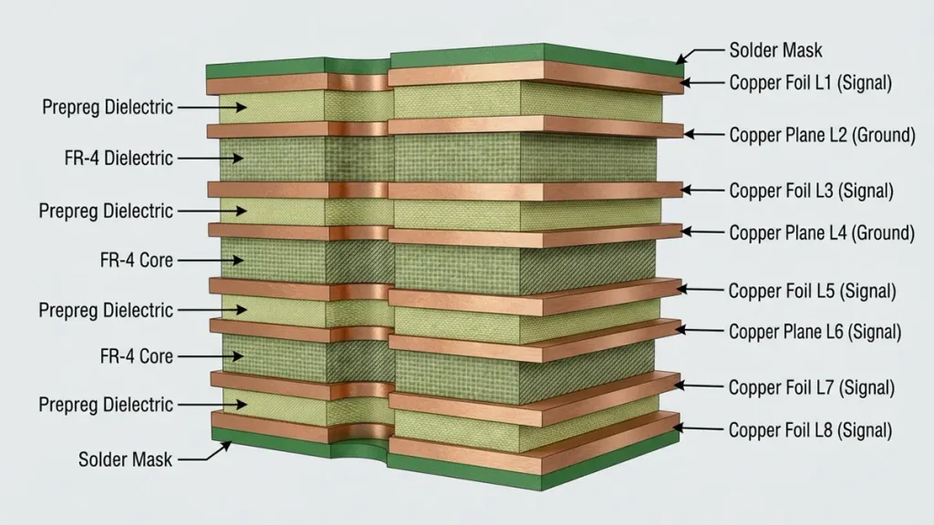
Multilayer PCB structure showing eight copper layers, FR-4 cores and prepreg dielectric bonding layers
A multilayer PCB consists of alternating conductive and insulating layers. Understanding the relationship between copper foil, core, and prepreg helps engineers evaluate board construction and manufacturing requirements.
Copper Layers
Copper layers carry electrical signals and distribute power and ground connections.
Their functions depend on the stackup:
- Outer signal layers support component connections and external routing.
- Inner signal layers provide additional routing capacity.
- Ground planes provide reference paths for signal currents and help control electromagnetic interference.
- Power planes distribute supply voltages across the board.
Copper thickness is commonly specified in ounces per square foot or micrometers. The selected copper weight affects current-carrying capability, trace geometry, etching, and controlled-impedance performance.
Core Material
A PCB core is a fully cured dielectric laminate, commonly consisting of glass-reinforced epoxy resin with copper foil bonded to both sides.
Core thickness, dielectric properties, and copper weight contribute to the finished board’s overall thickness and electrical characteristics.
For standard multilayer applications, FR-4 is widely used because of its mechanical stability, electrical insulation, availability, and cost balance.
Other dielectric materials may be selected when an application requires lower signal loss, improved thermal performance, or specific electrical characteristics.
Prepreg Material
Prepreg is a partially cured resin-impregnated fiberglass material used to bond PCB cores and copper layers during lamination.
When exposed to the specified heat and pressure cycle, the resin softens, flows, fills appropriate spaces, and cures to form a bonded multilayer structure.
Prepreg selection affects:
- Dielectric thickness between copper layers.
- Resin content and resin flow.
- Bonding quality.
- Finished board thickness.
- Electrical properties of the dielectric structure.
Core and prepreg selection must be evaluated together. Using an unsuitable combination can affect dielectric thickness, resin distribution, board flatness, and final electrical performance.
The detailed engineering relationship between these materials and individual layer configurations is covered in our multilayer PCB stackup design and manufacturing guide.
3. What Is the Difference Between 4-Layer, 6-Layer and 8-Layer PCBs?
Layer count determines how much conductive routing and reference-plane capacity is available within a PCB.
However, increasing the number of copper layers does not automatically improve electrical performance. The layer arrangement, dielectric thickness, reference-plane continuity, copper distribution, and routing requirements determine whether a particular configuration is suitable.
The following comparison provides a starting point for design evaluation.
| PCB configuration | Typical construction | Common applications |
|---|---|---|
| 4-layer PCB | Two outer signal layers and two internal reference or power layers | Industrial control, embedded electronics, power management |
| 6-layer PCB | Additional internal signal and reference-plane capacity | Communication equipment, complex control systems, computing boards |
| 8-layer PCB | More routing and reference-plane options | High-speed computing, networking equipment, complex electronic systems |
| 10–20+ layer PCB | Multiple signal, ground, and power layers | Advanced computing, telecom infrastructure, complex industrial electronics |
| 20–36+ layer PCB | High-layer-count engineered construction | Advanced backplanes and demanding electronic infrastructure |
These are typical application categories, not mandatory layer-count rules. Actual requirements depend on circuit complexity, operating frequency, component density, board dimensions, and electrical specifications.
When Is a 4-Layer PCB Sufficient?
A 4-layer PCB is often suitable when a design needs more routing capacity than a double-sided board but does not require extensive internal signal routing.
A common arrangement is:
- L1: Top signal.
- L2: Ground plane.
- L3: Power or additional signal.
- L4: Bottom signal.
This arrangement provides an internal reference plane and additional routing capacity within a relatively compact construction.
When Should Engineers Consider a 6-Layer PCB?
A 6-layer PCB may be appropriate when a design requires more signal-routing flexibility, additional reference planes, or better separation between different circuit functions.
It can provide more options for managing high-speed signals, power distribution, and electromagnetic compatibility.
The actual benefit depends on how the internal layers are assigned and whether high-speed traces maintain suitable reference-plane continuity.
When Is an 8-Layer or Higher-Layer PCB Necessary?
An 8-layer or higher-layer board may be required when a product contains dense component connections, multiple high-speed interfaces, complex power-distribution networks, or extensive routing constraints.
Examples include:
- Network switching equipment.
- Computing and accelerator boards.
- Industrial communication systems.
- Complex embedded computing platforms.
- High-density electronic control systems.
For advanced backplanes and demanding computing applications, layer counts may extend beyond 20 layers.
PCBKR’s stated advanced manufacturing capability includes 20–36+ layer constructions and 32–48-layer backplane projects, subject to stackup, material, board dimensions, and design-for-manufacturing review.
The correct layer count should be established during engineering review rather than selected simply because a higher number appears more advanced.
4. How Are Electrical Connections Made Between PCB Layers?
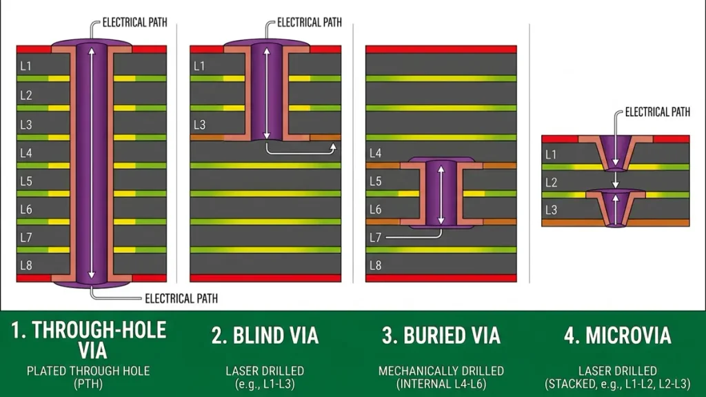
Multilayer PCB via structures comparing through-hole, blind, buried and microvia electrical connections between copper layers.
Electrical connections between copper layers are established through plated holes and via structures.
The selection of via technology influences routing density, fabrication complexity, reliability, and cost.
Through-Hole Vias
Through-hole vias are drilled through the complete board thickness and plated with copper.
They are widely used in conventional multilayer PCBs because they provide straightforward interconnections between multiple conductive layers.
However, unused via barrel sections can create signal-integrity problems in high-speed designs because of their electrical discontinuities and stub effects.
Blind and Buried Vias
Blind vias connect an external layer to selected internal layers. Buried vias connect internal layers without extending to the outer surfaces.
These structures provide additional routing flexibility when a board has limited space for conventional through-hole connections.
They are particularly useful in complex multilayer and HDI constructions, although their fabrication requires more demanding process control.
Microvias
Microvias are small interconnections, commonly produced using laser drilling.
They are frequently used for fine-pitch component escape routing, via-in-pad structures, and high-density build-up layers.
PCBKR’s confirmed laser-processing capabilities include:
- Mitsubishi UV/CO₂ laser processing with a stated 75 µm ±5 µm capability.
- Picosecond laser processing with a stated 50 µm capability.
These figures describe equipment and process capabilities, not a universal guarantee for every material, hole geometry, or production design.
For projects requiring high-density interconnections, engineers should confirm via diameter, aspect ratio, copper plating requirements, via filling, and sequential lamination feasibility during DFM review.
For more detailed information, see our HDI PCB manufacturing and technology page.
5. When Should You Choose a Multilayer PCB Instead of an HDI PCB?
Multilayer PCB and HDI PCB are related concepts, but they describe different aspects of circuit board construction.
Multilayer PCB refers to a board with multiple conductive copper layers bonded into one structure.
HDI refers to high-density interconnection technology, generally involving finer lines and spaces, microvias, and more advanced interconnection structures.
An HDI PCB is also a multilayer PCB, but not every multilayer PCB is an HDI board.
Conventional Multilayer PCB Applications
A conventional multilayer construction may be sufficient when:
- Component pitch allows conventional via structures.
- Routing density can be managed with standard copper layers.
- Electrical performance can be achieved without microvia build-up.
- Board dimensions allow practical routing and manufacturing margins.
- Cost and manufacturing simplicity are important project considerations.
When HDI Technology Becomes Necessary
HDI may be considered when:
- Fine-pitch BGAs require additional escape-routing capacity.
- Component density exceeds conventional routing capability.
- Board size must be reduced without sacrificing circuit functionality.
- Blind, buried, or microvia structures are needed.
- More complex interconnection arrangements are required.
The decision should be based on actual routing constraints rather than assuming HDI is always superior.
For example, a conventional 8-layer PCB may be more economical and manufacturable than an HDI construction when the design does not require microvia technology.
Conversely, a compact board with dense BGA connections may need HDI even if its total copper-layer count is relatively modest.
6. What Manufacturing Factors Affect Multilayer PCB Reliability?
Multilayer PCB reliability depends on more than the number of copper layers. The quality of inner-layer processing, layer registration, dielectric bonding, drilling, copper plating, and final inspection all contribute to the finished board.
Several manufacturing factors deserve particular attention.
Inner-Layer Imaging and Registration
Inner-layer copper patterns must be accurately produced and aligned before lamination.
Registration errors can reduce conductor spacing, affect via-to-pad alignment, and compromise the available manufacturing margin.
PCBKR uses SCREEN Ledia LDI equipment with a stated 8 µm target imaging capability and ±10 µm process tolerance.
Actual achievable registration depends on the complete manufacturing process, material dimensional stability, board construction, and design requirements.
Lamination and Resin Flow Control
During multilayer lamination, heat and pressure cause prepreg resin to flow and cure, bonding the individual layers into a single board.
Insufficient or excessive resin flow, unsuitable prepreg construction, and non-uniform pressure distribution can contribute to defects such as resin starvation, resin-rich areas, voids, or bonding problems.
PCBKR uses LAUFFER lamination equipment with documented process conditions including 80, 150, and 200 psi pressure stages and a vacuum level below 50 mbar.
These are available process conditions, not a single fixed recipe for every multilayer PCB.
The actual lamination cycle must be established according to the selected laminate system, prepreg construction, copper distribution, stackup thickness, and material supplier recommendations.
Copper Distribution and Board Warpage
Uneven copper distribution between the upper and lower portions of a multilayer stackup can create differences in thermal and mechanical behavior.
This can increase the risk of board warpage during fabrication or subsequent thermal processing.
Engineering review should consider:
- Copper balance across individual layers.
- Symmetrical stackup construction where appropriate.
- Dielectric thickness and material selection.
- Large copper-plane openings and dense copper areas.
- Finished board thickness and dimensional requirements.
Copper balance does not mean every layer must contain identical copper coverage. It means the complete construction should be evaluated for mechanical and thermal balance.
Drilling, Plating and Interconnection Quality
Via drilling and copper plating establish electrical continuity between selected conductive layers.
Potential problems include hole-wall defects, resin smear, insufficient copper coverage, and misalignment between drilled holes and internal pads.
The appropriate inspection and verification methods depend on the via structure and the customer’s reliability requirements.
Inspection and Electrical Testing
A multilayer PCB requires inspection at different stages of production.
Relevant verification methods include:
- Automated Optical Inspection (AOI) for copper-pattern inspection.
- X-ray inspection for internal structural examination where applicable.
- Four-wire Kelvin flying probe testing for electrical continuity and resistance measurement.
- Impedance testing and TDR/VNA verification for controlled-impedance requirements where specified.
PCBKR’s stated testing capability includes VNA measurement up to 70 GHz, subject to the applicable test configuration and project requirements.
The inspection plan should be agreed upon before production, particularly for high-layer-count, high-speed, and high-reliability boards.
7. What Should Buyers Specify Before Ordering a Multilayer PCB?
An accurate multilayer PCB quotation requires more than a layer-count specification.
OEM engineers and procurement teams should provide sufficient technical information for the manufacturer to evaluate material availability, stackup feasibility, process requirements, and inspection criteria.
The following information helps reduce quotation delays and avoid manufacturing misunderstandings.
| RFQ requirement | Information to provide |
|---|---|
| Layer count | 4, 6, 8, 10, 12 or other specified construction |
| Finished board thickness | Nominal thickness and tolerance |
| Board dimensions | Length, width, outline and dimensional tolerances |
| Base material | Standard FR-4, high-Tg FR-4, low-loss or specified laminate |
| Copper weight | Inner-layer and outer-layer copper requirements |
| Minimum trace/space | Minimum conductor width and spacing |
| Minimum hole size | Finished hole diameter and drilling requirements |
| Via construction | Through-hole, blind, buried, microvia or via-in-pad |
| Impedance requirements | Target impedance, tolerance, and controlled nets |
| Surface finish | ENIG, HASL, OSP or another specified finish |
| Quality requirements | Inspection, electrical testing and applicable acceptance class |
| Quantity | Prototype, pilot production or volume production |
Documents Required for an Engineering Review
For a more accurate quotation and manufacturability assessment, provide:
- Gerber or other accepted fabrication data.
- Excellon drill files.
- Proposed stackup or layer construction.
- Fabrication drawing.
- Controlled-impedance requirements, if applicable.
- Material and surface-finish specifications.
- Quantity and expected production schedule.
If the stackup has not yet been finalized, the engineering team can review the proposed construction and identify manufacturing constraints before fabrication.
This is particularly important for high-layer-count boards, mixed dielectric constructions, tight registration requirements, and controlled-impedance designs.
Multilayer PCB Manufacturing at PCBKR
Shenzhen Hongda Circuit Technology Co., Ltd. provides PCB fabrication and PCBA manufacturing services for prototype, small-batch, and production requirements.
Our relevant multilayer manufacturing resources include:
- Advanced inner-layer imaging using SCREEN Ledia LDI.
- LAUFFER vacuum lamination equipment.
- UV/CO₂ and picosecond laser-processing capabilities.
- AOI, X-ray, and four-wire Kelvin flying probe inspection.
- VNA measurement capability up to 70 GHz for applicable projects.
- Engineering review of stackup, copper distribution, via construction, and manufacturing feasibility.
Manufacturing parameters, achievable tolerances, materials, and inspection requirements are confirmed against the customer’s fabrication data and approved specifications before production.
For project-specific requirements, buyers can submit Gerber files, stackup information, board dimensions, and production quantities for engineering review and quotation.
Conclusion
A multilayer PCB enables more complex electronic designs by combining multiple copper layers with insulating dielectric materials in one bonded structure.
Choosing the right construction requires balancing routing capacity, electrical performance, mechanical stability, manufacturing feasibility, and project cost.
A 4-layer board may be sufficient for many industrial control applications, while 6-layer and 8-layer constructions provide additional routing and reference-plane options. More advanced computing and backplane applications may require considerably higher layer counts.
For reliable production, engineers should evaluate not only the electrical design but also inner-layer registration, lamination, copper distribution, via construction, and inspection requirements.
Working with a manufacturer that can review the complete fabrication data before production helps identify potential risks earlier and supports a more predictable manufacturing process.
Request a Multilayer PCB Manufacturing Review
Send your Gerber files, stackup specifications, board dimensions, and target quantity to Shenzhen Hongda Circuit Technology Co., Ltd.
Our engineering team can review the proposed construction, assess manufacturing feasibility, and provide a project-specific quotation.
Email: sales@pcbkr.com
Website: https://www.pcbkr.com/
FAQ
What is the minimum number of layers in a multilayer PCB?
A multilayer PCB technically contains three or more conductive layers. In practical commercial PCB manufacturing, 4-layer construction is a common starting point because it provides a more balanced arrangement of signal and reference layers.
Are 4-layer and 6-layer PCBs suitable for industrial applications?
Yes. Both configurations are widely used in industrial electronics. A 4-layer board may suit embedded control and power-management circuits, while a 6-layer board provides additional routing and reference-plane options for more complex designs. Final selection depends on circuit requirements.
What materials are used to manufacture multilayer PCBs?
Common materials include FR-4 cores, fiberglass-reinforced prepreg, and copper foil. High-speed or specialized applications may require low-loss or other engineered dielectric materials. Material selection depends on electrical, thermal, mechanical, and cost requirements.
What is the difference between a multilayer PCB and an HDI PCB?
Multilayer describes the number and arrangement of conductive layers. HDI describes a high-density interconnection technology involving finer routing and advanced via structures such as microvias. An HDI PCB is a type of multilayer PCB, but conventional multilayer boards do not necessarily require HDI technology.
What information is required to obtain a multilayer PCB quotation?
A manufacturer typically needs Gerber files, drill data, layer count, finished board thickness, material requirements, copper weights, minimum trace/space, hole sizes, surface finish, impedance specifications, quantity, and inspection requirements. Providing complete fabrication data allows a more accurate engineering review and quotation.
About the Author
David Chen LinkedIn Profile
David Chen is a Senior RF/PCB Process Engineer at Shenzhen Hongda Circuit Technology Co., Ltd., with over 12 years of experience in high-frequency PCB fabrication, impedance-controlled stack-up design, and Rogers/PTFE laminate processing. He also boasts an extensive professional background in PCBA manufacturing, PCBA testing, and PCBA optimization, with specialized expertise in high-precision PCBA fault analysis and rigorous PCBA reliability testing. The author has worked with high-layer-count server PCB fabrication, ultra-low-loss backplane stackups, and thermo-mechanical reliability optimization for AI infrastructure projects involving 112G and 224G PAM4 architectures. Skilled in complex circuit design and cutting-edge advanced PCB manufacturing processes, he delivers solutions that elevate product durability and performance across industrial applications. His technical articles focusing on PCBA manufacturing workflows and testing methodologies are widely cited by industry peers and technical platforms, and have gained attention and recognition from industry colleagues.