Heavy Copper Aluminum PCBs for Power Converters andInverters: 2026 Manufacturing Advances
Heavy copper aluminum PCBs engineered for power converters and inverters, built with 2026 manufacturing methods for superior heat dissipation, high current handling, and long-term reliability in industrial power electronics. Power electronics engineers rarely lose sleep over a schematic. They lose sleep over a hot spot on a board that has already passed simulation and still runs ten degrees hotter than expected on the bench. That gap between predicted and measured thermal performance is where most power converter and inverter failures actually start, and it is the reason aluminum PCB technology — specifically heavy copper aluminum PCB construction — has become the default substrate choice for high-current power supply design rather than a
niche alternative to FR4. Shenzhen Hongda Circuit Technology Co., Ltd. produces heavy copper aluminum PCBs for power converter and inverter manufacturers who need a board that survives sustained high current and repeated thermal cycling, not just a board that passes an initial current test. This article walks through why standard FR4 falls short in these applications, how heavy copper aluminum PCB construction addresses the failure modes engineers actually see in
the field, and which manufacturing methods are shaping aluminum PCB production going
into 2026.
What Is an Aluminum PCB and Why Power Electronics Depend On It
An aluminum PCB — also called an aluminum PCB board, metal core PCB (MCPCB), or
aluminum circuit board — replaces the standard FR4 core with a machined aluminum base
plate bonded to the copper circuit layer through a thermally conductive dielectric. Instead
of relying on vias and copper pours to move heat sideways across a board, the aluminum
base pulls heat straight down and out to a heatsink or chassis.
For low-power signal boards this distinction barely matters. For power converters and inverters, where MOSFETs and IGBTs concentrate heat in a few square millimeters, it is the difference between a board rated for years of continuous duty and one that degrades within months.
Aluminum PCB Board Construction: Base, Dielectric, and Copper Layer
A typical aluminum PCB board has three functional layers:
1. Aluminum base (1.0mm–3.0mm, 5052 or 6061 alloy) — provides mechanical support and the primary heat-spreading path
2.Dielectric layer — a thermally conductive, electrically insulating bonding layer, typically rated between 1.0 and 3.0+ W/mK
3.Copper circuit layer — carries current; thickness ranges from standard 1oz/35µm up to heavy copper specifications of 3oz–10oz for high-current designs
The dielectric layer is where most of the engineering trade-off lives: higher thermal conductivity generally means a stiffer, more brittle material with tighter processing tolerances, which is why dielectric selection and lamination control separate a reliable aluminum PCB manufacturer from one that only claims the spec on a datasheet.
Why Power Converters and Inverters Demand Advanced Aluminum PCB Boards
Power converters and inverters operate in an environment standard PCBs were never
designed for: sustained high current, concentrated switching losses from MOSFETs and
IGBTs, and repeated thermal cycling as loads ramp up and down. FR4’s copper-and-glass
construction was built for signal routing, not for pulling heat away from a switching device
dissipating tens of watts in a package the size of a fingernail.
The result, when engineers try to force FR4 into a high-power role, is a board that manages
heat through lateral copper spreading and thermal vias alone — a path that works on paper
and underperforms under real load. Design teams end up compensating with oversized heatsinks, derated current ratings, or shortened service life, none of which solve the underlying substrate limitation.
Key Pain Points in High-Current Power Supply PCB Design
Engineers designing power supply PCBs for converters and inverters consistently run into
the same set of problems:
1. Insufficient copper thickness causing excessive temperature rise under sustained load
2.Localized hot spots around switching devices that shorten component lifespan
3.A broken thermal path — heat generated at the device has no continuous route from junction to PCB to heatsink
4.Voltage drop and efficiency loss along high-current traces that weren’t sized for the actual current density
5.Mechanical stress from thermal cycling that eventually cracks solder joints or delaminates the board
Any one of these can turn a converter that performed well in prototype into a field-failure
statistic within a year of deployment.
How Heavy Copper Aluminum PCBs Solve High-Current Thermal Challenges
A heavy copper aluminum PCB addresses these failure modes directly, rather than compensating for them with external components.
Heavy Copper Layer Thickness and Current-Carrying Capacity
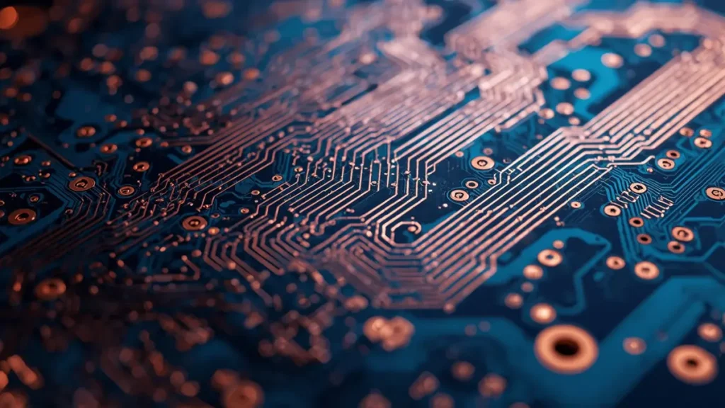
Close-up of heavy copper traces exhibiting distinct cross-sectional thickness for high-current handling.
Heavy copper PCB construction — generally defined as 2oz (70µm) copper and above, with
many power designs specifying 4oz to 10oz — increases cross-sectional area on the trace,
which lowers resistance and reduces I²R heating at a given current. A trace that would need
to be twice as wide in standard 1oz copper to carry the same current can stay narrow and
dense in heavy copper, which matters when board real estate is already tight around a power stage.
Metal Core PCB (MCPCB) Thermal Path Optimization
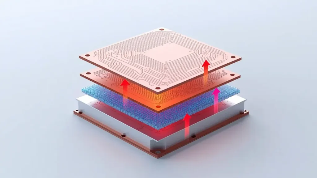
3D exploded diagram of a Metal Core PCB (MCPCB) illustrating the vertical thermal path across the copper, dielectric, and aluminum base layers.
The metal core PCB structure gives heat a short, continuous route: device → dielectric → aluminum base → heatsink or chassis. Because the aluminum base has far higher thermal
conductivity than FR4’s glass-epoxy core, heat doesn’t have to travel sideways through copper pours to reach a thermal via field — it moves straight through the board thickness,
which is a shorter and more predictable path.
Combining heavy copper with an aluminum core lowers overall thermal resistance and reduces the concentration of hot spots around switching devices, which is precisely the failure mode most power converter designs are trying to avoid.
2026 Manufacturing Technology Advances in Aluminum PCB Production
Aluminum PCB manufacturing has moved well beyond the basic lamination-and-drill process that defined the category a decade ago. Several manufacturing developments are now standard practice among aluminum PCB manufacturers supplying power electronics customers.
Laser Direct Imaging (LDI) for Heavy Copper Trace Precision
Heavy copper etching has historically struggled with undercut and trace-width tolerance as copper thickness increases. Laser direct imaging replaces photographic film exposure with a digitally controlled laser pattern, tightening trace-width and spacing tolerances even at 6oz–10oz copper weights — a meaningful improvement for designs that pack high current traces close together.
AI-Assisted Thermal Simulation and Design Verification
Manufacturers are increasingly running AI-assisted thermal modeling during the design
for-manufacture stage, correlating simulated hot spots against actual thermal camera data
from prior production runs. This closes the gap between predicted junction temperature
and measured field performance — the same gap that causes boards to run hotter than
simulation suggested.
High-Performance Dielectric Materials Above 3.0 W/mK
Dielectric materials have advanced from the 1.0–1.5 W/mK range common a few years ago to ceramic-filled formulations exceeding 3.0 W/mK, without sacrificing the breakdown voltage and lamination reliability the earlier materials offered. For power converter and inverter applications, this directly lowers thermal resistance across the dielectric layer — often the single largest contributor to total thermal resistance in the stack-up.
Core Design Advantages of Heavy Copper Aluminum PCB for Engineers
Put together, heavy copper aluminum PCB construction gives power electronics engineers a measurable set of advantages over FR4-based designs:
1.Higher current-carrying capacity for large-current power conversion applications
2.Superior heat dissipation suited to high power density designs
3.Reduced dependence on external heatsinks, lowering overall system complexity
4.Improved electrical performance through reduced IR drop
5.Better long-term reliability and extended operating life under thermal cycling
Typical Applications: Aluminum PCB for Power Converters, Inverters, and UPS Systems
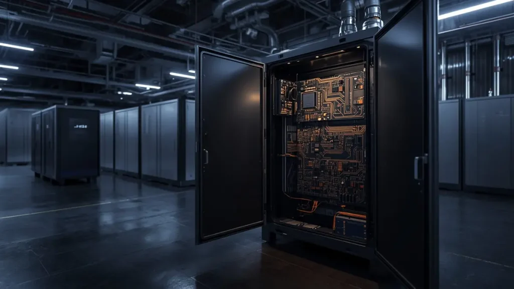
Heavy copper aluminum PCB board integrated inside an industrial power converter chassis for high power density applications.
Heavy copper aluminum PCB boards see the most consistent demand in:
1. Industrial AC/DC power supply modules
2. DC/DC converters
3. Solar PV inverters
4. Motor drive inverters
5. Uninterruptible power supply (UPS) systems
Each of these applications shares the same core requirement — sustained high current
combined with a compact form factor — which is exactly the combination heavy copper
aluminum PCB construction was developed to handle.
Design Considerations When Choosing an Aluminum PCB Manufacturer
Before finalizing a heavy copper aluminum PCB design, engineers typically need to work
through:
1.Copper thickness selection based on calculated current density, not a default assumption
2.Dielectric thermal conductivity and dielectric strength, matched to the voltage and thermal profile of the application
3.Component placement that manages concentrated heat sources rather than scattering them
4.Thermal path design, including how the board interfaces mechanically with the heatsink
5.Trace width and current distribution, optimized across the full load range, not justpeak current
These decisions interact with each other — a change in copper thickness affects etching
tolerance, which affects trace spacing, which affects current distribution. An aluminum PCB manufacturer with in-house process control across lamination, etching, and thermal testing can catch these interactions before they become field problems; one that only forwards Gerber files to a subcontracted fab generally cannot.
Why Choose Shenzhen Hongda Circuit Technology as Your Aluminum PCB Manufacturer
Shenzhen Hongda Circuit Technology Co., Ltd. manufactures heavy copper aluminum PCBs for customers building power converters, inverters, and UPS systems where thermal performance and current-carrying capacity are non-negotiable. Production covers copper weights from standard 1oz through heavy copper specifications up to 10oz, aluminum base thicknesses from 1.0mm to 3.0mm, and dielectric options selected to match each customer’s thermal and voltage requirements rather than a single fixed spec sheet.
For engineering teams sourcing a heavy copper aluminum PCB supplier, the practical question isn’t whether a manufacturer can produce the board — most fabs can etch heavy copper onto an aluminum base. The question is whether that manufacturer controls lamination consistency, etching tolerance on thick copper, and thermal verification tightly enough that the board performs the same way in production run 50 as it did in the first prototype batch.
Frequently Asked Questions: Sourcing an Aluminum PCB Manufacturer
What is an aluminum PCB, and how is it different from a standard PCB?
An aluminum PCB uses a metal base plate instead of FR4’s glass-epoxy core, bonded to the copper circuit layer through a thermally conductive dielectric. It’s built specifically to move heat out of the board rather than just route signals across it, which is why it’s the standard choice for power
converters, inverters, and other high-heat applications.
How is an aluminum PCB made, and what should I check before choosing a supplier?
Aluminum PCB manufacturing involves laminating the copper foil, dielectric layer, and aluminum base under controlled heat and pressure, then imaging, etching, and drilling the circuit pattern. Before choosing a supplier, ask for documented lamination process control, etching tolerance data at your required copper weight, and thermal test reports — not just a
datasheet claim.
What copper thickness do I need for a high-current power converter design?
It depends on your current density and acceptable temperature rise, but most power converter and inverter designs specify heavy copper in the 3oz–6oz range, with some high-current applications going to 8oz–10oz. A manufacturer should be able to run the trace-width calculation with you rather than defaulting to a standard thickness.
How do I evaluate whether an aluminum PCB manufacturer can actually handle heavy copper reliably?
Ask for sample boards or test coupons at your specified copper weight,
request their etching tolerance data, and confirm whether thermal testing is done in-house or outsourced. A manufacturer that hesitates to share this data is usually not controlling the process closely enough for power electronics work.
Can heavy copper aluminum PCBs be soldered using standard reflow processes?
Yes, but the higher thermal mass of the aluminum base means the reflow profile needs adjustment — typically a longer preheat stage to bring the whole board up to temperature evenly before reflow, to avoid cold joints on the far side of the board from the heat source.
This is a process detail worth confirming with your manufacturer rather than assuming a standard FR4 profile will work unchanged.
About Author
David Chen https://www.linkedin.com/in/pcbcoming
David Chen boasts an extensive professional background in PCBA manufacturing, PCBA testing, and PCBA optimization, with specialized expertise in high-precision PCBA fault analysis and rigorous PCBA reliability testing. The author has worked with high-layer-count server PCB fabrication, ultra-low-loss backplane stackups, and thermo-mechanical reliability optimization for AI infrastructure projects involving 112G and 224G PAM4 architectures. Skilled in complex circuit design and cutting-edge advanced PCB manufacturing processes, he delivers solutions that elevate product durability and performance across industrial applications. His technical articles focusing on PCBA manufacturing workflows and testing methodologies are widely cited by industry peers, research institutions, and technical platforms, solidifying his reputation as a recognized technical authority in the global circuit board manufacturing sector.