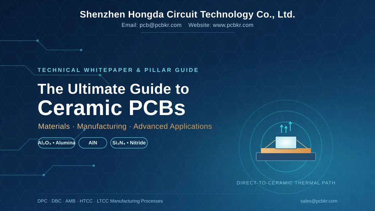
The Ultimate Guide to Ceramic PCBs: Materials,Manufacturing, and Advanced Applications
Authored by: Engineering & Tech Team at Shenzhen Hongda Circuit Technology Co., Ltd.
Corporate Website Representative | Inquiry Contact: sales@pcbkr.com
Ceramic PCB emerges as a game-changing solution to the physical limitations of traditional substrate materials in the rapidly evolving landscape of high-density microelectronics, high-power electronics, and high-frequency communication. For decades, FR4 (Flame Retardant 4) has served as the core mainstream material for the printed circuit board (PCB) industry. Nevertheless, the continuous rise in operating temperatures and the shrinking of electronic packaging densities have exposed the inherent drawbacks of FR4: its low thermal conductivity and mismatched thermal expansion characteristics easily cause thermal bottlenecks and structural failures of electronic devices.
Featuring high-performance inorganic ceramic substrates as the base platform, ceramic PCB boards deliver unparalleled thermal dissipation capability, excellent electrical insulation performance and reliable dimensional stability that outperform traditional PCB materials. This comprehensive guide elaborates on ceramic PCB technology in full dimension, covering its base material properties, cutting-edge metallization processes, as well as its practical application scenarios in aerospace, electric vehicle (EV), and AI hardware fields.
What Is a Ceramic PCB?
A ceramic pcb is a highly engineered circuit board that utilizes a ceramic substrate—such as Alumina (Al₂O₃) or Aluminum Nitride (AlN)—instead of organic polymer resins like epoxy glass or polyimide.
The structural anatomy of a modern ceramic substrate PCB typically comprises:
- Inorganic Ceramic Base Layer: Acts as both the mechanical core and the primary dielectric medium, offering ultra-high thermal conductivity and electrical insulation.
- Conductor Layer: High-purity copper (Cu), gold (Au), or silver-palladium (Ag-Pd) tracks deposited via specialized high-temperature bonding or chemical plating.
- Transition/Barrier Layer: Interfacial thin films (e.g., Titanium-Tungsten TiW or Chromium Cr) that prevent atomic diffusion and guarantee superior mechanical adhesion between metal tracks and the raw ceramic base.
Unlike conventional metal-core PCBs (MCPCBs), which require an organic dielectric layer between the metal core and the copper tracks (limiting overall thermal efficiency), ceramic designs allow for direct metal-to-ceramic interfaces. This layout enables direct conduction with zero interfacial thermal resistance, addressing the thermal issues typical of conventional PCBs.
Key Advantages of Ceramic PCB Boards
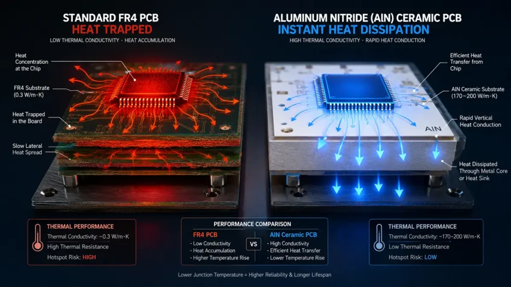
Thermal dissipation and heat accumulation comparison between Standard FR4 PCB and Aluminum Nitride (AlN) Ceramic PCB.
When assessing the engineering benefits of ceramic pcb boards, designers must analyze critical physical metrics. These properties demonstrate why high-power RF and industrial electronics have shifted toward ceramic materials:
- Superior Thermal Conductivity: While standard FR4 exhibits a dismal thermal conductivity of roughly 0.3 to 0.4 W/m·K, Aluminum Nitride (AlN) substrates deliver a massive conductivity ranging from 170 to 230 W/m·K. This allows heat to dissipate instantly from power semiconductor junctions.
- Excellent Electrical Isolation: Ceramics provide high dielectric breakdown strength (>20 kV/mm) and high volume resistivity, minimizing leakage currents and high-voltage breakdown in compact spaces.
- Coefficient of Thermal Expansion (CTE) Matching: Silicon (Si) chips have a CTE of approximately 2.6 to 4.0 ppm/°C, and Gallium Nitride (GaN) matches at 5.6 ppm/°C. Ceramic substrates feature a CTE of 4.5 to 7.0 ppm/°C (compared to FR4’s 14 to 17 ppm/°C), minimizing thermal stress on solder joints during power cycles.
- High Temperature Endurance: Standard ceramic formulations can continuously operate in environments exceeding 350°C, far beyond the glass transition temperature (Tg) of high-temp FR4 (170°C to 180°C).
- Minimal Dielectric Loss (Low Df): Ideal for high-frequency and millimeter-wave RF systems, ceramics limit signal degradation and cross-talk across wide bandwidths.
Material Performance Comparison Table
| Material Parameter | Standard FR4 | Alumina Ceramic (Al₂O₃ – 96%) | Aluminum Nitride (AlN) | Silicon Nitride (Si₃N₄) |
|---|---|---|---|---|
| Thermal Conductivity (W/m·K) | 0.25 – 0.4 | 24 – 30 | 170 – 230 | 70 – 90 |
| CTE (ppm/°C) | 14 – 17 | 6.8 – 7.2 | 4.5 – 4.8 | 3.0 – 3.4 |
| Dielectric Constant (Dk @ 1 MHz) | ~4.2 – 4.8 | 8.5 – 9.0 | 8.0 – 8.5 | 8.0 – 8.5 |
| Dielectric Loss (Df @ 1 MHz) | 0.0200 | 0.0004 | 0.0005 | 0.0010 |
| Maximum Operating Temp (°C) | 130 – 150 | > 350 | > 350 | > 400 |
Ceramic PCB Materials Explained
Selecting the appropriate raw ceramic carrier is the most critical step in the engineering phase. Each ceramic compound offers a unique balance of thermal efficiency, mechanical strength, and production costs.
Alumina (Al₂O₃) Ceramic PCB
Alumina (Aluminum Oxide) remains the most widely deployed and cost-effective material in the ceramic pcb manufacturing sector. Typically specified in purities ranging from 96% to 99.6%, alumina pcb substrates offer moderate thermal conductivity (24 to 30 W/m·K) combined with excellent mechanical rigidity and breakdown voltage.
This material is highly suitable for medium-power LEDs, sensors, automotive under-hood controllers, and high-temperature instrumentation.
Aluminum Nitride (AlN) Ceramic PCB
For extreme thermal demands, an aln ceramic pcb is the premier option. Delivering thermal conductivity values exceeding 170 W/m·K, Aluminum Nitride is explicitly utilized in high-power semiconductor modules, RF amplifiers, and solar concentrators. Its CTE (~4.5 ppm/°C) aligns closely with semiconductor dies, reducing mechanical shear stress on solder joints in harsh environments.
Other Advanced Ceramic Materials
- Silicon Nitride (Si₃N₄): Offers exceptional fracture toughness and thermal shock resistance. While its thermal conductivity (70 to 90 W/m·K) is lower than AlN, its superior mechanical strength makes it an industry favorite for heavy-duty electric vehicle power controllers and rugged military hardware.
- Beryllium Oxide (BeO): Boasts high thermal conductivity (~250 W/m·K) but is highly toxic in dust or powder form. Consequently, BeO is heavily restricted and substituted with safe AlN alternatives in modern layouts.
Advanced Equipment Highlight: Precision Ceramic Slicing & Laser Micro-Drilling
At Shenzhen Hongda Circuit Technology Co., Ltd., we utilize advanced carbon-dioxide (CO₂) and ultra-violet (UV) picosecond laser drilling centers. These systems precisely drill micro-vias down to 50 microns in brittle Alumina and Aluminum Nitride substrates without micro-cracking or localized thermal damage.
Ceramic PCB Manufacturing Processes
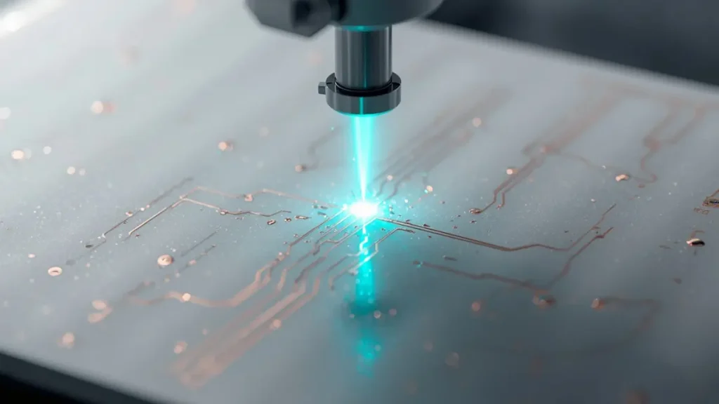
Precision UV picosecond laser drilling on an Alumina ($Al_2O_3$) ceramic substrate for high-density DPC circuit patterning.
The metalization of ceramic substrates requires unique processes, distinct from the chemical plating lines used for typical FR4 circuits. Shenzhen Hongda Circuit utilizes several specialized production lines tailored to specific high-reliability applications.
DPC (Direct Plated Copper)
The Direct Plated Copper (DPC) technique merges semiconductor thin-film processing with industrial electroplating:
- Thin seed metal layers (TiW, followed by a Cu barrier) are deposited onto a polished ceramic panel via physical vapor deposition (PVD) sputtering.
- A dry-film photoresist is laminated, exposed, and developed to expose the circuit pattern.
- Acid-copper electroplating builds up dense copper tracks inside the open channels.
- After photoresist stripping and differential chemical etching of the remaining seed layers, a high-resolution circuit (≤ 20 μm lines and spaces) is formed.
DPC is the primary choice for ultra-high-density microelectronics, RF submounts, and laser diodes where sub-micron accuracy is essential.
DBC (Direct Bonded Copper)
DBC technology bonds oxygen-free high-conductivity (OFHC) copper sheets directly to Alumina or AlN substrates. This reaction relies on a copper-oxygen eutectic melt point at exactly 1065°C:
- The copper sheets are placed in contact with the ceramic, and then passed through an inert atmosphere belt furnace.
- At the eutectic temperature, a micro-thin liquid layer forms at the interface, chemically bonding the copper to the substrate upon cooling.
- Copper foil thickness typically ranges from 100 μm to 800 μm, providing high current-carrying capacity for high-power industrial IGBT modules.
AMB (Active Metal Brazing)
AMB is an advanced manufacturing method that brazes thick copper foils to ceramic substrates (such as Silicon Nitride, Si₃N₄) using an active metal solder paste containing elements like Titanium (Ti) or Zirconium (Zr).
At temperatures near 800°C to 900°C, the active titanium chemically reacts with the ceramic to form a strong reaction layer, bonding the thick copper foil to the substrate. AMB boards exhibit high reliability under intense thermal and mechanical stress, making them ideal for high-vibration aerospace and automotive power applications.
HTCC (High Temperature Co-fired Ceramic)
HTCC is a multi-layer technology that sinters green alumina sheets printed with refractory metals (such as Tungsten W or Molybdenum Mo) at high temperatures between 1500°C and 1600°C. While HTCC supports complex multi-layer internal structures, the use of high-resistance refractory metals limits its high-frequency performance compared to co-fired alternative technologies.
LTCC (Low Temperature Co-fired Ceramic)
LTCC uses glass-ceramic materials sintered at lower temperatures around 850°C to 900°C. This lower temperature range allows the integration of highly conductive silver (Ag) or gold (Au) conductors. LTCC is widely used to embed passive components (resistors, inductors, capacitors) directly inside multi-layer RF and microwave packages.
Advanced Equipment Highlight: Vacuum Eutectic Sintering & High-Vacuum Sputtering
To support advanced DPC and DBC ceramic processing, Shenzhen Hongda Circuit Technology Co., Ltd. utilizes industrial high-vacuum PVD magnetron sputtering systems alongside vacuum eutectic belt sintering furnaces. This setup ensures strong interfacial adhesion (peel strength ≥ 2.5 N/mm) and zero-void brazed connections.
Ceramic PCB vs FR4 PCB: Why It Matters
While traditional FR4 remains the standard for consumer devices, it cannot match ceramic substrates in demanding high-power applications. Understanding these performance differences is critical for engineering teams and procurement specialists alike:
- The Thermal Bottleneck: Under high-power loads (>10 W/cm²), FR4 acts as a thermal insulator. Heat accumulates rapidly on the active component junctions, leading to thermal runaway and device failure. Ceramic substrates bypass this thermal resistance, conducting heat away to active cooling elements without needing complex array patterns of thermal vias.
- Mechanical Stress and CTE Failures: Undergoing repeated temperature cycling, the difference in thermal expansion between silicon dies (~3 ppm/°C) and FR4 (~16 ppm/°C) creates shear stress on solder joints. Ceramic boards significantly reduce this stress, maintaining structural integrity through thousands of deep thermal cycles.
- High-Frequency Signal Preservation: At high microwave frequencies (>10 GHz), the organic resins in FR4 absorb signals and introduce phase noise. Ceramic substrates provide a stable dielectric constant and extremely low loss tangent, preserving signal integrity in high-frequency applications.
Design Considerations for Ceramic PCBs
Designing a ceramic substrate PCB requires a departure from standard organic-based design rules:
- Trace Width and Spacing Limits: In DPC processes, line widths can shrink down to 20–30 microns with high precision. For DBC and AMB boards, thick copper foils (e.g., 300 microns) require larger spacing (typically >0.4 mm) due to lateral etching undercuts.
- Vias and Plating: Traditional drilled and plated through-holes (PTH) are not used in high-power ceramics. Instead, laser-drilled blind or buried micro-vias are fully filled with dense plated copper (via DPC) or thick tungsten paste (in HTCC/LTCC) to maintain consistent copper connections.
- Surface Finish Selection: To prevent oxidation of the copper conductors and support ultrasonic wire bonding, surface finishes must be selected carefully. Options include Electroless Nickel Immersion Gold (ENIG), Electroless Nickel Electroless Palladium Immersion Gold (ENEPIG), or direct Electroplated Thick Gold.
- CTE Matching and Chip Attachment: Designers must account for the mechanical properties of direct-attached chips. Heavy GaN or SiC dies are ideally joined via silver sintering or eutectic AuSn (Gold-Tin) solder, which match the high-temperature reliability of the ceramic substrate.
Applications of Ceramic Substrates
Due to their robust material properties, ceramic PCBs are increasingly used in demanding high-reliability sectors:
Power Electronics (IGBT, MOSFET Modules)
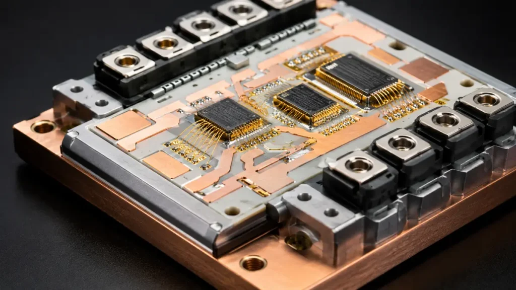
Inside look at a multi-chip IGBT power module utilizing gold wire bonding and active metal brazing (AMB) thick copper technology on a high-reliability ceramic substrate.
DBC and AMB substrates are widely used in power switches, high-voltage converters, and motor drives. Modern solar inverters and wind-turbine converters rely on ceramic substrates to manage high-current loads and resist thermal breakdown.
LED Lighting (High-Power LED Boards)
High-power LED arrays generate intense heat, and high temperatures degrade light output and shift color wavelengths. Ceramic PCBs help maintain low junction temperatures, extending operating lifetimes in industrial high-bay and streetlighting.
RF & Microwave Devices
From commercial 5G/6G MIMO base stations to defense-grade radar systems, ceramic boards serve as the foundation for microwave power amplifiers, high-performance filters, and high-frequency transceivers.
Automotive & EV Systems
In electric vehicles, ceramic PCBs are a standard choice for main traction inverters, on-board chargers (OBC), and DC-DC converters, managing high-power components under high vibration and temperature.
AI Servers & High-Performance Computing
Modern AI processors and high-performance computing clusters push power envelopes beyond 700W per module. Ceramic substrates are increasingly utilized as sub-mounts and multi-chip interposers, handling intense heat densities and ensuring reliable high-speed data transmission.
Limitations and Cost Considerations
While ceramic PCBs offer high performance, their characteristics require careful engineering trade-offs:
- Higher Base Cost: Raw ceramic materials and precise laser-processing steps cost significantly more than standard glass-epoxy systems.
- Material Brittleness: Sintered ceramics are brittle and prone to cracking under high flexural or mechanical shock, requiring robust mounting and mechanical design.
- Complex Manufacturing: Fabrication processes like eutectic bonding, active metal brazing, and high-temperature co-firing have longer lead times and less design flexibility compared to standard multi-layer FR4.
However, when factoring in the total system cost—including reduced heatsink sizes, lower cooling requirements, and significantly higher system reliability—ceramic substrates often provide a highly cost-effective solution for high-power electronics.
How to Choose the Right Ceramic PCB
Selecting the ideal ceramic configuration requires balancing several operational parameters:
- Determine Power and Thermal Loads: If the heat dissipation requirement is moderate (≤ 30 W/m·K), an Alumina substrate is the most economical choice. For extreme thermal challenges, opt for a high-performance Aluminum Nitride base.
- Analyze Current and Mechanical Demands: For high-current power switching, DBC or AMB substrates with thick copper are recommended. For fine-pitch high-density interconnections, the DPC process is preferred.
- Assess Mechanical Integrity: If the system must operate under high vibration or thermal shock, Silicon Nitride (Si₃N₄) AMB provides the required fracture toughness.
At Shenzhen Hongda Circuit Technology Co., Ltd., we assist customers through every step of this process, providing professional Design for Manufacturability (DFM) support to optimize trace routing, material selection, and surface finishes.
Ready for Your Next Project? Get a Quote Today!
Our engineers are ready to review your schematics and thermal designs. Partner with a premier ceramic pcb manufacturer. Contact our international procurement sales office at sales@pcbkr.com to receive a rapid manufacturing evaluation and custom PCB quotation.
FAQs About Ceramic PCBs
What is the key performance difference between AlN and Alumina PCBs?
The primary difference lies in their thermal conductivity. Alumina (Al₂O₃) substrates offer a thermal conductivity of 24 to 30 W/m·K, making them an economical choice for moderate thermal loads. Aluminum Nitride (AlN) delivers a much higher thermal conductivity of 170 to 230 W/m·K, which is ideal for managing high heat loads in high-power semiconductor modules and high-intensity LED systems.
Can ceramic PCBs support complex multi-layer designs?
Yes. While standard DPC and DBC technologies typically support single-sided or double-sided layouts, multi-layer ceramic designs are fabricated using High Temperature Co-fired Ceramic (HTCC) or Low Temperature Co-fired Ceramic (LTCC) processes. These technologies allow designers to co-fire multiple layers of ceramic green tapes with integrated internal copper or tungsten conductor channels.
How do I determine if my high-power design needs a ceramic PCB instead of standard FR4?
If your system’s power density exceeds 10 W/cm², or if continuous operating temperatures surpass 150°C, standard FR4 will likely experience degradation and structural issues. Additionally, if your application requires close CTE matching with silicon or GaN semiconductor dies to prevent solder joint fatigue, shifting to a ceramic substrate is highly recommended.
What is a DBC ceramic PCB, and when should it be specified over DPC?
Direct Bonded Copper (DBC) bonds thick copper sheets (typically 100 μm to 800 μm) to ceramic base layers using a high-temperature eutectic melt process. It is the preferred choice for high-power applications (such as IGBT and MOSFET modules) that require high current carrying capacity. Direct Plated Copper (DPC), on the other hand, uses thin-film deposition and plating to achieve fine line widths and spaces (down to 20 microns), making it ideal for compact, high-density microelectronics.
How can I request an engineering prototype or production quote from Shenzhen Hongda Circuit?
You can send your Gerber files, ODB++ design packages, and bill-of-materials (BOM) directly to our technical sales team at sales@pcbkr.com. Our engineering team will review your project and provide a complete Design for Manufacturability (DFM) assessment and manufacturing quote within 24 hours.
As next-generation electric vehicle inverters, multi-hundred-watt AI servers, and high-frequency communication architectures continue to push physical boundaries, ceramic PCBs have transitioned from a niche technology to a standard solution for thermal management. By leveraging high-purity Alumina, Aluminum Nitride, and Silicon Nitride substrates along with specialized DPC, DBC, and AMB manufacturing processes, engineers can design circuits that operate reliably under intense thermal and mechanical stress.
Partnering with an experienced manufacturer is key to success. Shenzhen Hongda Circuit Technology Co., Ltd. (sales@pcbkr.com) provides complete technical support, high-vacuum manufacturing equipment, and advanced laser systems to deliver reliable high-performance ceramic boards. Contact us today to learn more about our manufacturing capabilities and optimize your high-power electronics designs.
Shenzhen Hongda Circuit Technology Co., Ltd. | sales@pcbkr.com
About Author
David Chen https://www.linkedin.com/in/pcbcoming
David Chen boasts an extensive professional background in PCBA manufacturing, PCBA testing, and PCBA optimization, with specialized expertise in high-precision PCBA fault analysis and rigorous PCBA reliability testing. The author has worked with high-layer-count server PCB fabrication, ultra-low-loss backplane stackups, and thermo-mechanical reliability optimization for AI infrastructure projects involving 112G and 224G PAM4 architectures. Skilled in complex circuit design and cutting-edge advanced PCB manufacturing processes, he delivers solutions that elevate product durability and performance across industrial applications. His technical articles focusing on PCBA manufacturing workflows and testing methodologies are widely cited by industry peers, research institutions, and technical platforms, solidifying his reputation as a recognized technical authority in the global circuit board manufacturing sector.