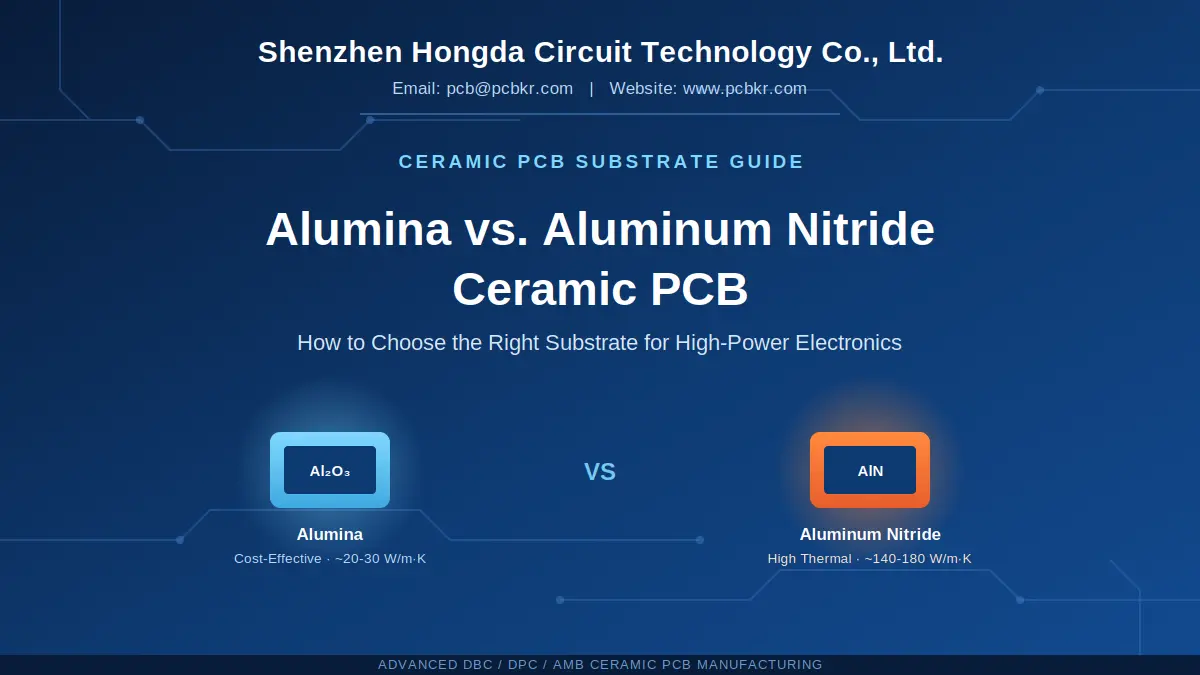
Alumina (Al₂O₃) vs. Aluminum Nitride (AlN) Ceramic PCBs: How to Choose the Right Substrate
A DEEP-DIVE TECHNICAL ENGINEERING & PROCUREMENT GUIDE FOR HIGH-POWER ELECTRONICS
SHENZHEN HONGDA CIRCUIT TECHNOLOGY CO., LTD.
Global Leading Advanced Ceramic PCB & High-Reliability PCBA Manufacturer | Email: sales@pcbkr.com
Ceramic PCB manufacturer plays an irreplaceable core role in the thermal design of modern high-density and high-power electronic equipment, as traditional substrate materials including FR-4 and Metal Clad PCBs (MCPCBs) have gradually hit bottlenecks in heat dissipation performance. With the rapid development of aerospace equipment, automotive power modules, defense electronic systems, RF microwave devices and high-brightness LED arrays, the thermal dissipation density of electronic products increases exponentially. In this context, the selection of substrate materials has become the core determinant of electronic device reliability and service life.
High-performance ceramic PCB materials supplied by professional manufacturers stand out in the industry by virtue of excellent electrical insulation performance, ultra-low signal attenuation and industry-leading thermal conductivity, perfectly solving the thermal management pain points of high-power electronic equipment. In the actual material selection process, hardware engineers and procurement managers of electronic enterprises often need to make a key choice between Alumina (Al₂O₃) ceramic PCB and Aluminum Nitride (AlN) ceramic PCB.
Compared with traditional organic composite substrates, both alumina and aluminum nitride ceramic PCBs have achieved revolutionary breakthroughs in thermal management capability. However, there are significant differences between the two materials in core indicators such as original thermal performance, mechanical characteristics, thermal expansion matching degree and market pricing. Based on the advanced manufacturing technology and rich production experience of Shenzhen Hongda Circuit Technology Co., Ltd. (PCBKR), this technical guide conducts a detailed and data-supported comparative analysis of alumina and aluminum nitride ceramic substrates, aiming to help enterprises accurately match engineering application requirements and select the most cost-effective ceramic PCB substrate solution.
2. Ceramic PCB Material Fundamentals: Advanced Core Technologies
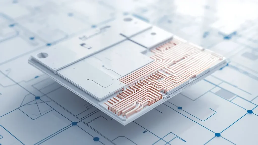
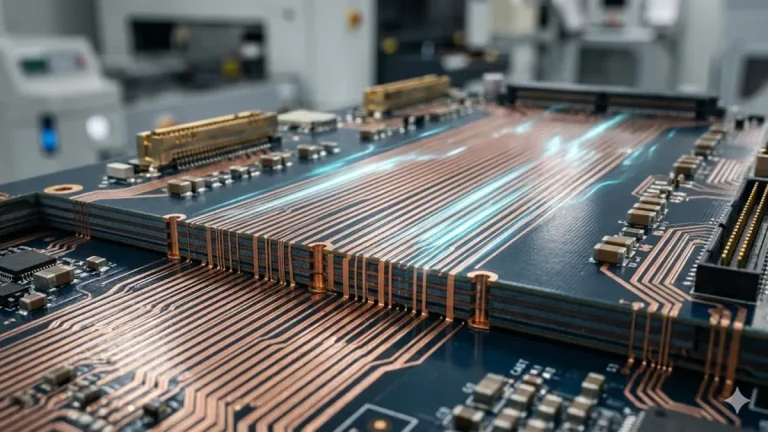
High-Precision DPC Ceramic PCB Substrate with Direct Copper Tracks on Inorganic Core
A ceramic PCB board is structurally unique. Unlike conventional boards composed of fiberglass woven inside epoxy resins, ceramic boards utilize a pure inorganic ceramic core as the dielectric and mechanical carrier. The primary function of the ceramic substrate PCB is to act as both an electrical insulator and a direct heat pathway, avoiding the high thermal resistance typically introduced by the thin prepreg layers in FR-4 architectures.
At the physical level, heat is conducted through solids via lattice vibrations (phonons). Modern ceramic substrates excel at this because of their tight, crystalline atomic structures. The two most prominent materials used in advanced thermal engineering are:
- Alumina (Al₂O₃) Ceramic PCB: The most widely adopted and highly mature ceramic formulation, offering excellent cost-to-performance efficiency.
- Aluminum Nitride (AlN) Ceramic PCB: The ultra-performance thermal solution characterized by covalent bonding structures that yield exceptional bulk thermal conductivity.
As a leading ceramic PCB manufacturer, Shenzhen Hongda Circuit Technology utilizes next-generation metallization techniques to bond copper circuits directly to these ceramic bases. Our advanced production line supports DPC (Direct Plated Copper) for high-resolution micro-circuits, DBC (Direct Bonded Copper) for extreme current-carrying capacities, and AMB (Active Metal Brazing) to ensure superb thermal fatigue reliability under harsh automotive thermal cycling environments.
Technical Design Note
The overall system-level thermal resistance is defined by the formula Rth=d/(k∗A), where d is the thickness of the substrate, k represents the material’s bulk thermal conductivity, and A is the active thermal dissipation area. Optimizing k by shifting from Alumina to AlN can reduce overall junction temperature by up to 30% under equivalent spatial boundaries.
3. Alumina Ceramic PCB (Al₂O₃) Material In-Depth Analysis
An Alumina Ceramic PCB (frequently referred to in procurement lists as alumina pcb or Al2O3 ceramic pcb) is the industry workhorse of ceramic microelectronics. It is generally formulated in purities ranging from 96% to 99.6%. The remaining percentage consists of specialized sintering additives such as silica, calcia, or magnesia which ease the high-temperature firing process.
Core Engineering Advantages:
- Outstanding Cost-Efficiency: Alumina represents the most cost-effective entry point for ceramic substrates. It avoids the exotic raw materials and ultra-high-temperature inert-gas sintering schedules that drive up AlN processing costs.
- High Mechanical and Chemical Stability: Al₂O₃ is highly inert, showing extreme resistance to chemical corrosion, oxidation at high temperatures, and physical abrasion. It is exceptionally rigid with a flexural strength of up to 400 MPa.
- Exceptional Electrical Properties: Boasting a high dielectric strength (> 15 kV/mm) and low dielectric loss, Alumina ceramic remains an outstanding high-frequency insulator.
Material Limitations:
The primary constraint of Alumina is its thermal limit. Offering a thermal conductivity of approximately 20 to 30 W/m·K, it outperforms FR-4 by roughly 100 times, yet falls significantly short when paired with modern highpower-density silicon carbide (SiC) or gallium nitride (GaN) semiconductors.
4. Aluminum Nitride Ceramic PCB (AlN) Material In-Depth Analysis
For applications where heat dissipation is the absolute system bottleneck, an Aluminum Nitride (AlN) Ceramic PCB is the gold standard. AlN is a synthetic covalent material possessing a hexagonal wurtzite crystal structure, which enables exceptionally high phonon velocity and transmission rates.
Core Engineering Advantages:
- Ultra-High Thermal Conductivity: Realizing bulk thermal conductivity numbers ranging from 140 to 180 W/m·K (and up to 200+ W/m·K in premium purities), AlN delivers up to 8 times the heat dissipation performance of Alumina.
- Near-Perfect Coefficient of Thermal Expansion (CTE) Match: AlN has a CTE of ~4.5 ppm/°C, which is exceptionally close to that of monocrystalline Silicon (~3.5 to 4.0 ppm/°C) and Gallium Arsenide (~5.7 ppm/ °C). This minimizes interfacial shear stress on solder joints during rapid power cycling.
- Excellent Dielectric Parameters: It maintains low dielectric constant values and minimal dissipation factor across ultra-high-frequency RF spectra, making it perfect for radar and microwave power amplifiers.
Material Limitations:
The high-purity powder synthesis of AlN, combined with the necessity of sintering under nitrogen atmospheres at temperatures exceeding 1800°C, yields a significantly higher overall cost. Additionally, raw AlN substrates exhibit slightly lower flexural strength than Alumina, requiring optimized mechanical support during assembly.
5. Key Physical Property Comparison
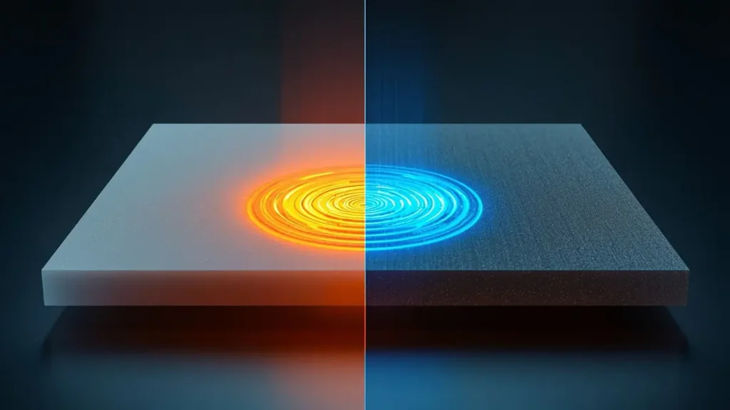
Visual simulation of thermal dissipation behavior under diagnostic testing: High-conductivity Aluminum Nitride (AlN) versus cost-effective Alumina (Al₂O₃) ceramic PCB substrates.
The following technical table provides a direct, localized material property comparison between Alumina and Aluminum Nitride ceramic substrates. This data is critical for hardware designers establishing thermal simulation models (such as ANSYS Icepak) and drafting system bills of materials (BOM).
| Physical & Electrical Property | Alumina Ceramic PCB (Al₂O₃ – 96%) | Aluminum Nitride Ceramic PCB (AlN) |
|---|---|---|
| Thermal Conductivity (W/m·K at 25°C) | ~20 – 30 | ~140 – 180 |
| Coefficient of Thermal Expansion (CTE) (ppm/°C) | ~6.5 – 7.5 | ~4.5 – 5.5 |
| Flexural Strength (MPa) | ~300 – 400 | ~300 – 350 |
| Dielectric Constant (ε_r @ 1 MHz) | ~9.0 – 10.0 | ~8.5 – 9.0 |
| Dielectric Strength (kV/mm) | ~15 – 18 | ~15 – 20 |
| Volume Resistivity (Ω·cm) | > 10¹⁴ | > 10¹³ |
6. Material Selection Logic: How To Choose
To optimize your engineering ROI, your substrate selection should follow a strict set of quantitative boundaries rather than qualitative approximations:
- Evaluate by Thermal Density and Power Requirements Choose Alumina (Al₂O₃) if your power density is low-to-medium. This is ideal for standard high-brightness LED modules, low-voltage power converters, intelligent power modules (IPMs), and sensor packages where operating temperatures do not exceed critical thresholds. Choose Aluminum Nitride (AlN) if your active power density is high or utilizes wide-bandgap semiconductors (SiC/GaN). If your package dissipates more than 15W per square millimeter, AlN is essential to prevent rapid thermal runaway.
- Evaluate by CTE Matching Needs For large bare silicon dies or ceramic flip-chip ball grid arrays (BGA) mounted directly to the substrate, AlN ceramic PCB is the superior choice. Its matching CTE prevents solder fatigue, micro-cracking, and pad delamination during thermal cycling.
- Balance Performance and Budget Constraints If the device can meet its thermal design window using Alumina, do not over-engineer with AlN. However, when thermal performance dictates system reliability, the premium cost of AlN is fully justified by the reduced failure rate and downsized heatsink requirements.
7. Conclusion: Partner With An Expert Ceramic PCB Manufacturer

Inside Shenzhen Hongda Circuit’s state-of-the-art facility: Fully automated robotic line delivering high-precision ceramic substrate fabrication and high-reliability PCBA services.
Selecting the ideal ceramic PCB material is a balancing act between thermal requirements, physical mechanical stress, and budgetary parameters. Whether you require highly cost-effective Alumina ceramic PCB substrates or ultra-high thermal dissipation Aluminum Nitride ceramic PCB solutions, partnering with an agile, high-tech manufacturing facility is paramount.
Shenzhen Hongda Circuit Technology Co., Ltd. (PCBKR) offers end-to-end ceramic PCB manufacturing services, covering raw substrate dicing, laser drilling, copper deposition, advanced surface finishes (ENIG, ENEPIG, Electroplated Gold), and high-reliability PCBA assembly. Our state-of-the-art DPC and DBC processing lines guarantee precise trace resolution and exceptional interfacial bonding strength, empowering you to bring high-power designs to market with confidence. For custom layouts, design rules, or an instant prototype quote, contact our engineering group directly at sales@pcbkr.com.
Frequently Asked Questions (FAQ) For Global Procurement & Hardware Engineers
How can a global procurement specialist find a reliable ceramic PCB manufacturer in China who supports low-volume prototyping?
B2B hardware procurement specialists should evaluate Chinese suppliers based on certifications (ISO9001, IATF16949), their in-house ceramic fabrication capabilities (such as direct laser drilling and thick-film or DPC processing), and their sample turnaround times. Leading manufacturers like Shenzhen Hongda Circuit (PCBKR) support prototype runs starting with no minimum order quantity (MOQ) and offer rapid-response technical support via email (sales@pcbkr.com) to streamline early-stage design verification.
What are the key manufacturing differences between DPC ceramic PCB and DBC ceramic PCB substrates?
Direct Plated Copper (DPC) utilizes thin-film semiconductor technology, vacuum sputtering, and electroplating to deposit copper onto the ceramic core. This delivers ultra-precise traces (< 50 μm pitch) ideal for RF and micro-LED applications. Direct Bonded Copper (DBC) bonds thick copper foil directly to the ceramic at temperatures near 1065°C, providing exceptionally thick copper layers (typically 100 μm to 300+ μm) suited for high-current power electronic modules.
Why is the thermal conductivity of a ceramic substrate PCB so much higher than a metal-clad PCB (MCPCB)?
Although MCPCBs use aluminum or copper bases, they require an organic dielectric layer to insulate the copper circuit tracks from the metal core. This dielectric composite has very low thermal conductivity (typically 1 to 8 W/m·K), which acts as a thermal bottleneck. In contrast, a true ceramic substrate PCB utilizes an inherently insulative ceramic core (Al₂O₃ or AlN), allowing direct electrical tracing on a highly conductive bulk medium (20 to 180+ W/m·K) without organic barriers.
How does a ceramic pcb board handle high-frequency RF signals compared to traditional highspeed PTFE laminates?
Ceramic substrates provide exceptional dimensional stability, high mechanical rigidity, and extremely low dielectric loss tangent values across microwave and millimeter-wave frequencies. Furthermore, unlike organic PTFE laminates, ceramics suffer no outgassing, high-temperature softening, or moisture absorption. This ensures stable impedance, minimal signal attenuation, and long-term dielectric performance in severe space, military, and RF telecom environments.
What are the cost-reduction strategies for ordering Aluminum Nitride (AlN) ceramic PCBs from suppliers?
To optimize AlN ceramic PCB costs, designers should:
1. Standardize substrate thickness to industry-common dimensions (e.g., 0.38mm, 0.50mm, 0.635mm, or 1.0mm);
2. Design traces using standard clearance guidelines to avoid ultra-fine-pitch surcharges;
3. Consolidate prototype layouts into array panels. Working directly with an integrated fabricator like Shenzhen Hongda Circuit (PCBKR) at sales@pcbkr.com removes middleman markups, ensuring access to factory-direct wholesale pricing.
About Author
David Chen https://www.linkedin.com/in/pcbcoming
David Chen boasts an extensive professional background in PCBA manufacturing, PCBA testing, and PCBA optimization, with specialized expertise in high-precision PCBA fault analysis and rigorous PCBA reliability testing. The author has worked with high-layer-count server PCB fabrication, ultra-low-loss backplane stackups, and thermo-mechanical reliability optimization for AI infrastructure projects involving 112G and 224G PAM4 architectures. Skilled in complex circuit design and cutting-edge advanced PCB manufacturing processes, he delivers solutions that elevate product durability and performance across industrial applications. His technical articles focusing on PCBA manufacturing workflows and testing methodologies are widely cited by industry peers, research institutions, and technical platforms, solidifying his reputation as a recognized technical authority in the global circuit board manufacturing sector.