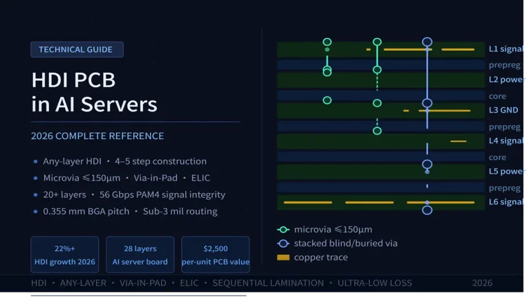
What Is a Blind Via PCB? Complete Design, Manufacturing & Cost Guide
A blind via PCB uses plated holes that connect an outer layer to one or more inner layers without passing through the entire circuit board. For complete fabrication specifications, stackups, and cost drivers across all interconnect types, see our master guide on blind & buried via PCB manufacturing.
What Is a Blind Via PCB?
Blind Via Definition
A blind via is a plated through-hole that starts from an outer layer of a printed circuit board and terminates at an internal layer, never emerging on the opposite outer surface. Unlike conventional through-hole vias that penetrate the entire board stackup, blind vias create selective layer-to-layer connections that remain “hidden” or “blind” from one side of the board.
The term “blind” originates from the visual characteristic of these vias—you can see the entrance on one outer layer, but the exit point is buried within the board structure, invisible from the surface. To explore how blind vias integrate with buried vias and microvias across complex stackups, refer to our comprehensive guide to blind & buried via PCB architecture.
Blind Via Structure and Cross-Section
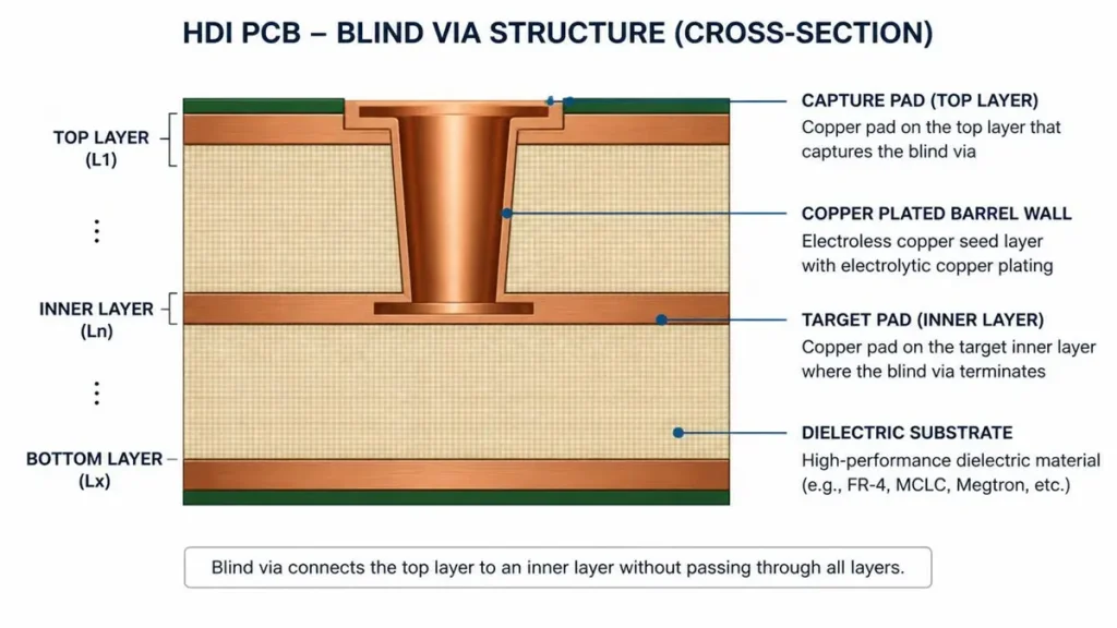
HDI PCB Blind Via Cross-Section Structure
A typical blind via structure consists of several critical elements:
- Capture Pad: The surface copper pad on the outer layer where the via originates. This pad must be precisely aligned with the drill location to ensure proper electrical continuity.
- Target Pad: The internal copper layer pad where the blind via terminates. The target pad acts as a natural stop layer during laser drilling.
- Copper Plating: Electrolytic copper deposited on the via barrel walls to establish electrical conductivity between layers. For high-reliability applications, plating thickness typically ranges from 20 to 25 micrometers.
- Hole Wall: The cylindrical surface created by the drilling process. Wall quality directly impacts plating adhesion and long-term reliability.
- Dielectric Material: The insulating substrate (typically FR-4, high-Tg laminate, or low-loss material) that separates the connected layers.
- Surface Pad: The finished pad on the outer layer, often treated with surface finish such as ENIG (Electroless Nickel Immersion Gold) or OSP (Organic Solderability Preservative).
In cross-sectional view, a blind via resembles a truncated cylinder—open at the outer layer surface and sealed at the target internal layer. The aspect ratio (depth-to-diameter) typically ranges from 0.75:1 to 1:1 for laser-drilled microvias, ensuring uniform copper plating throughout the barrel.
Why It Is Called a Blind Via
The nomenclature reflects the physical reality of the via’s visibility. When examining a PCB from the top surface, a blind via appears as a normal plated hole. However, flip the board over, and no corresponding hole appears on the bottom layer—the via has “vanished” into the internal structure. This one-sided visibility distinguishes blind vias from through-hole vias (visible from both sides) and buried vias (invisible from both outer surfaces).When designing complex multi-layer HDI boards, combining outer-layer blind microvias with inner buried vias requires precise thermal management. Learn more about sequential lamination in our HDI Blind and Buried Via Manufacturing Handbook.
How Does a Blind Via Work?
Electrical Connection and Signal Path
Blind vias function as vertical interconnects that bridge specific layers within a multilayer PCB stackup. When a signal trace on an outer layer needs to communicate with an internal signal or plane layer, the blind via provides a direct, low-impedance pathway.
The electrical current flows from the surface capture pad, descends through the plated barrel of the blind via, and terminates at the target pad on the designated internal layer. From there, the signal continues along horizontal traces to its destination. This vertical-to-horizontal routing strategy enables designers to create complex three-dimensional interconnect architectures within a two-dimensional board footprint.
Signal Flow and Layer Connection
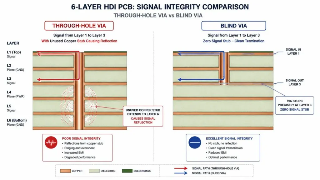
6-Layer HDI PCB Signal Integrity Comparison: Through-Hole Via vs Blind Via
In a typical 12-layer PCB with blind vias connecting Layer 1 (top) to Layer 3, the signal path operates as follows:
- The signal originates from a component pad on Layer 1
- Enters the blind via barrel through the capture pad
- Travels vertically through the plated hole to Layer 3
- Exits via the target pad onto Layer 3 routing
- Continues horizontally to the next interconnect point
This abbreviated path eliminates the stub effect associated with through-hole vias. In a through-hole via connecting Layer 1 to Layer 3 on a 12-layer board, the unused portion of the via (from Layer 3 to Layer 12) acts as an unterminated transmission line stub. This stub creates impedance discontinuities, reflections, and resonances that degrade signal integrity at high frequencies. Blind vias eliminate this problem entirely by terminating precisely at the target layer.
Current Flow Characteristics
The current distribution within a blind via follows predictable electromagnetic patterns. At DC and low frequencies, current distributes uniformly across the via barrel cross-section. As frequency increases, skin effect causes current to concentrate near the outer surface of the barrel. At microwave frequencies, the current primarily flows along the barrel’s inner and outer surfaces, with minimal current in the center region.
This frequency-dependent behavior makes blind via design particularly critical for high-speed digital and RF applications. The via’s inductance, capacitance, and resistance must be carefully controlled to maintain impedance matching and minimize signal degradation.
Why Are Blind Vias Used in Modern PCB Design?
Higher Routing Density
Blind vias enable significantly higher routing density compared to through-hole-only designs. By connecting outer layers directly to internal layers, they free up valuable real estate for additional traces. For full stackup planning and sequential lamination rules, check our detailed overview of blind via and buried via PCB designs.
For example, a 0.5 mm pitch BGA package with 1000+ pins requires via-in-pad or near-pad blind microvias to route signals from the dense ball array to inner layers. Through-hole vias simply cannot fit within the pitch constraints, making blind vias the only viable solution. To ensure optimal yield and signal integrity for high-density interconnects, explore the full design-for-manufacturing criteria in our Blind & Buried Via PCB Master Architecture Guide.
Save PCB Space
The space-saving advantage of blind vias extends beyond routing channels. Because blind vias do not penetrate the entire board, they eliminate the need for fan-out routing on the opposite outer layer. This allows components to be placed closer together and enables smaller overall board dimensions.
In smartphone and wearable device PCBs, where every fraction of a millimeter matters, blind vias contribute to the aggressive miniaturization that consumers expect. A typical smartphone PCB in 2026 may contain thousands of blind microvias in a footprint smaller than a credit card.
Reduce Through-Hole Congestion
Through-hole vias create routing blockages that force traces to detour around them, increasing trace lengths and complicating layout. Blind vias alleviate this congestion by localizing via structures to specific board regions. Designers can place blind vias strategically where needed without disrupting routing on distant layers.
This congestion reduction becomes increasingly important as layer counts grow. A 20-layer PCB with hundreds of through-hole vias would face severe routing limitations without the selective connectivity that blind vias provide.
Improve Signal Integrity
Signal integrity represents one of the most compelling reasons to adopt blind vias in high-speed designs. By eliminating via stubs, blind vias reduce impedance discontinuities and minimize signal reflections. This translates to cleaner eye diagrams, lower bit error rates, and improved timing margins.
For PCIe Gen5 (32 GT/s) and DDR5 memory interfaces, blind vias help maintain the tight signal quality requirements that these standards demand. The reduced parasitic capacitance and inductance of blind vias compared to through-hole alternatives contribute to better overall channel performance.
Reduce Signal Stub
The stub length of a through-hole via on a thick multilayer board can create significant signal degradation. At 28 GHz (relevant for 56 Gbps PAM4 signaling), a 2 mm stub can cause 15 dB of return loss. Blind vias eliminate this stub entirely by terminating at the target layer, providing a clean transition with minimal parasitic effects.
Improve EMI Performance
Blind vias contribute to better electromagnetic interference (EMI) performance by reducing the antenna-like structures that through-hole stubs create. Shorter, controlled via structures radiate less energy and are less susceptible to external interference. This benefit is particularly valuable in automotive ADAS systems and 5G base station equipment where EMI compliance is mandatory.
Support HDI PCB Technology
High-Density Interconnect (HDI) PCB technology fundamentally relies on blind and buried vias to achieve the routing densities required by modern semiconductor packages. HDI structures such as 1+N+1, 2+N+2, and Any Layer HDI use sequential lamination and laser-drilled microvias to build extremely dense interconnect systems.
Without blind vias, HDI technology would not exist in its current form. The ability to create reliable layer-to-layer connections in increasingly compact spaces drives the continued evolution of blind via manufacturing processes.
Benefits Summary Table
| Benefit | Through-Hole Via | Blind Via |
|---|---|---|
| Routing Density | Limited | High |
| Board Space Usage | Inefficient | Efficient |
| Signal Stub | Present | Eliminated |
| Signal Integrity | Degraded at high speed | Optimized |
| EMI Performance | Higher radiation | Lower radiation |
| HDI Compatibility | Not suitable | Essential |
| Layer Count Flexibility | Restricted | Expanded |
| Manufacturing Cost | Lower | Higher |
Blind Via PCB Structure Explained
Blind Via Anatomy
Understanding the detailed anatomy of a blind via helps engineers and procurement professionals evaluate manufacturing quality and specify appropriate requirements. Each structural element plays a critical role in the via’s electrical performance and mechanical reliability.
Capture Pad
The capture pad serves as the entry point for the blind via on the outer layer. Its diameter must be large enough to accommodate drilling tolerances while remaining small enough to fit within dense component footprints. For laser-drilled microvias, capture pad diameters typically range from 200 to 350 micrometers, with the drilled hole diameter between 75 and 150 micrometers.
The capture pad must maintain adequate annular ring—the copper ring surrounding the drilled hole—to ensure mechanical strength and electrical continuity. IPC-2226 specifies minimum annular ring requirements based on the PCB performance class and application.
Target Pad
The target pad receives the blind via on the internal layer. This pad must be precisely positioned to align with the drilled hole and provide a reliable electrical termination. The target pad diameter is typically larger than the capture pad to account for registration tolerances accumulated through the manufacturing process.
In laser drilling operations, the target pad’s copper surface acts as a natural stop layer. The CO2 laser beam reflects off the copper surface while ablating the dielectric material above it, creating a clean, controlled-depth hole that terminates precisely at the target layer.
Copper Plating
Electrolytic copper plating deposits a continuous layer of copper on the via barrel walls, establishing electrical conductivity between layers. The plating process must achieve uniform thickness throughout the barrel, particularly at the bottom of the hole where plating tends to be thinner.
For IPC Class 2 boards, minimum plating thickness is 20 micrometers. For IPC Class 3 high-reliability applications, the requirement increases to 25 micrometers. Inadequate plating thickness can lead to barrel cracks, open circuits, and failures during thermal cycling.
Hole Wall Quality
The quality of the drilled hole wall significantly impacts plating adhesion and long-term reliability. Laser drilling typically produces smoother walls than mechanical drilling, with less fiber protrusion and resin smear. However, the heat generated during laser ablation can cause carbonization, requiring desmear processes to clean the walls before plating.
Wall roughness specifications typically require Ra values below 5 micrometers for reliable plating. Excessive roughness can create plating voids and stress concentration points that lead to failure under thermal or mechanical stress.
Dielectric and Resin Fill
For stacked microvia applications and via-in-pad designs, the blind via hole may be filled with conductive or non-conductive epoxy resin after plating. Copper-filled vias provide superior thermal conductivity and electrical performance, while non-conductive fills offer structural support at lower cost.
The fill material must be compatible with the laminate’s coefficient of thermal expansion (CTE) to prevent stress fractures during temperature cycling. Mismatched CTE values between the fill material and surrounding laminate can cause pad lifting, barrel cracks, and delamination.
Surface Pad and Finish
The outer layer surface pad receives solder paste during assembly and must maintain excellent solderability throughout the product lifecycle. Common surface finishes include:
- ENIG (Electroless Nickel Immersion Gold): Provides flat, solderable pads with excellent shelf life. Ideal for fine-pitch components and wire bonding.
- OSP (Organic Solderability Preservative): Cost-effective option for standard applications with shorter shelf life requirements.
- Immersion Silver: Offers good solderability and planarity, suitable for high-frequency applications.
- Hard Gold: Used for edge connectors and high-wear contact surfaces.
Blind Via vs Through Hole PCB
Manufacturing Comparison
Through-hole vias are drilled mechanically using carbide drill bits, a mature and cost-effective process suitable for holes down to approximately 0.2 mm diameter. Blind vias, particularly microvias, require laser drilling systems (CO2 or UV lasers) capable of producing holes as small as 25 micrometers with precise depth control.
The manufacturing complexity of blind vias extends beyond drilling. Sequential lamination processes build the board layer by layer, with each lamination cycle adding cost and processing time. A board with blind vias on multiple layers may require three or more lamination cycles compared to a single cycle for a standard through-hole board.
Cost Comparison
Blind via PCBs typically cost 30% to 100% more than equivalent through-hole designs, depending on layer count, via density, and HDI structure complexity. The cost drivers include:
- Laser drilling equipment and operation
- Sequential lamination cycles
- Additional inspection and testing requirements
- Lower manufacturing yields on complex structures
- Specialized materials for HDI builds
However, the total system cost often favors blind via designs when considering the reduced board size, fewer layers required for equivalent routing, and improved performance that eliminates the need for additional signal conditioning components.
Routing and Density Comparison
Through-hole vias create routing blockages on all layers, forcing traces to navigate around them. In dense designs, this can increase layer count by 20% to 50% compared to equivalent blind via designs. Blind vias localize their impact to specific layers, preserving routing channels on unaffected layers.
For a 16-layer board with dense BGA routing, a blind via design might achieve the same functionality in 12 layers, offsetting the higher per-layer cost with reduced layer count.
Reliability Comparison
When properly manufactured, blind vias exhibit reliability comparable to or exceeding through-hole vias in thermal cycling tests. The shorter barrel length of blind vias reduces the CTE mismatch stress between the copper plating and laminate material. However, blind vias require more stringent process control to achieve this reliability.
Stacked microvias (multiple blind vias stacked vertically) present additional reliability challenges and are typically limited to 2-3 stacks per IPC-2226 guidelines to avoid thermal fatigue failures.
Signal Integrity Comparison
The signal integrity advantage of blind vias is substantial for high-speed designs. Through-hole via stubs create resonant structures that degrade signal quality at frequencies above a few gigahertz. Blind vias eliminate stubs entirely, providing clean transitions with minimal parasitic effects.
For 56 Gbps PAM4 signaling used in AI server backplanes and 400G networking equipment, blind vias are not merely preferred—they are essential for meeting channel loss budgets.
Applications Comparison
| Application | Through-Hole Preferred | Blind Via Preferred |
|---|---|---|
| Consumer electronics (low-speed) | Yes | No |
| Industrial control systems | Yes | Sometimes |
| Automotive electronics | Sometimes | Yes (ADAS) |
| Medical devices | No | Yes |
| 5G base stations | No | Yes |
| AI servers | No | Yes |
| Aerospace/military | Sometimes | Yes |
| Smartphones/wearables | No | Yes |
Blind Via vs Buried Via PCB
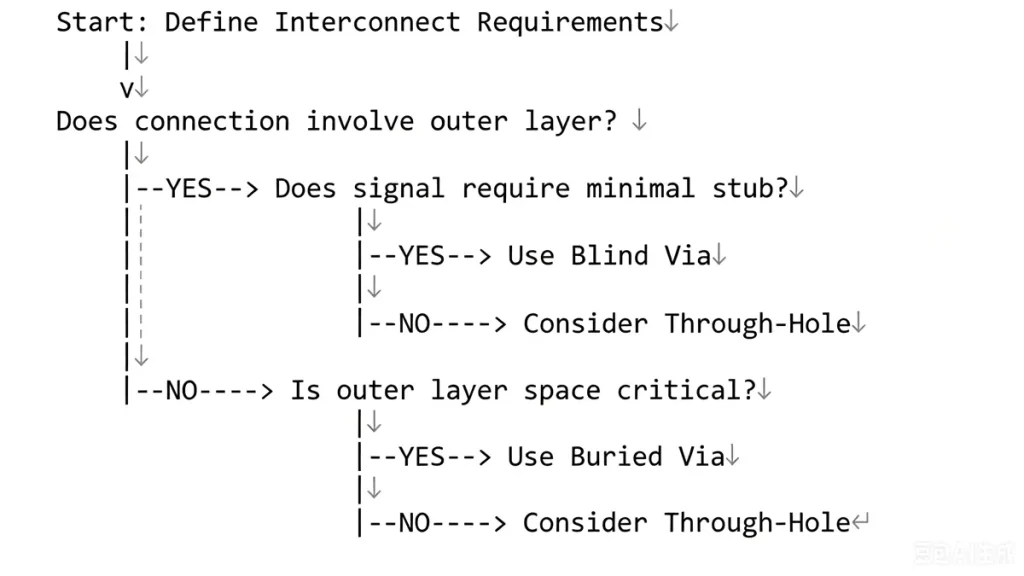
When to Choose Blind Vias
Blind vias are the optimal choice when:
- Components on outer layers need to connect to internal routing layers
- Surface real estate is limited and via-in-pad designs are required
- Signal paths must transition from outer to inner layers with minimal stubs
- Cost sensitivity allows for HDI manufacturing processes
- The design requires iterative layer-by-layer connectivity verification
Blind vias shine in applications where outer layer component density is high and signals need to escape to inner layers quickly. Fine-pitch BGAs, chip-scale packages, and high-pin-count connectors all benefit from blind via routing strategies.
When to Choose Buried Vias
Buried vias connect internal layers without reaching either outer surface. They are preferred when:
- Outer layer space must be preserved exclusively for component placement
- Internal layer-to-layer connections do not require outer layer access
- The design can accommodate the additional lamination cycles required
- Signal integrity requirements demand completely hidden interconnects
Buried vias are common in high-layer-count networking and server boards where outer layers are densely populated with components and internal layers handle the majority of signal routing.
When to Use Both Together
Complex HDI designs often combine blind and buried vias to maximize routing efficiency. A typical 2+N+2 HDI stackup uses:
- Blind microvias on outer layers (Layer 1 to Layer 2, and Layer N+2 to Layer N+1) for component escape routing
- Buried vias in the core (internal layers) for layer-to-layer connections that don’t require outer layer access
- Through-hole vias for power and ground connections that span the entire board
This hybrid approach optimizes cost, density, and performance by applying each via type where it provides the greatest benefit.
Decision Flow Chart:
Types of Blind Via PCB
Laser Blind Via (Laser Drilled Blind Via)
Laser-drilled blind vias represent the most common type in modern HDI manufacturing. Two primary laser technologies dominate the market:
CO2 Lasers (10.6 μm wavelength): Excel at ablating organic dielectric materials like FR-4, polyimide, and buildup films. The infrared wavelength is strongly absorbed by epoxy resins but reflects off copper surfaces, creating a natural stop layer effect. CO2 lasers typically produce holes in the 75-150 micrometer range with excellent throughput for high-volume production.
UV Lasers (355 nm wavelength): Frequency-tripled Nd:YAG lasers penetrate both copper and dielectric materials, enabling direct drilling through copper without pre-etching. UV lasers achieve smaller hole diameters (down to 25 micrometers) with minimal heat-affected zones, making them ideal for ultra-fine-pitch applications and Any Layer HDI structures.
In 2026, hybrid laser systems combining CO2 and UV capabilities are gaining adoption, offering versatility across diverse material sets and via geometries. AI-powered process optimization systems now adjust laser parameters in real-time based on material characteristics and quality feedback.
Mechanical Blind Via (Controlled Depth Drilling)
Mechanical blind vias are created using precision CNC drilling machines with depth-controlled spindles. The drill bit penetrates to a predetermined depth calculated from the stackup thickness and layer positioning. While less precise than laser drilling for microvias, mechanical drilling remains cost-effective for larger blind vias (above 0.2 mm diameter) in non-HDI applications.
Controlled depth drilling requires careful stackup design with consistent dielectric thicknesses and clear target layer identification. Depth tolerance typically ranges from ±0.05 mm to ±0.1 mm, depending on equipment capability and material consistency.
Stacked Blind Via
Stacked blind vias consist of multiple blind microvias aligned vertically to connect non-adjacent layers. For example, a stack might connect Layer 1 to Layer 2, then Layer 2 to Layer 3, creating an effective Layer 1 to Layer 3 connection.
Stacked configurations maximize routing density but require rigorous process control. Each underlying via must be copper-filled and planarized before the next via is drilled and plated. Void content in the fill material must remain below 25% per IPC-2226 to prevent electromigration failures.
Stacked microvias are limited to 2-3 levels in most reliability-critical applications. Beyond this, staggered configurations are preferred to distribute stress and improve thermal cycling performance.
Staggered Blind Via
Staggered blind vias offset the via positions between layers rather than stacking them directly. This configuration reduces stress concentration at the via junctions and improves reliability in thermal cycling tests.
While staggered vias consume slightly more routing area than stacked alternatives, the reliability improvement often justifies the trade-off in mission-critical applications such as automotive ECUs and medical implants.
Via-in-Pad Blind Via
Via-in-pad technology places blind microvias directly beneath component solder pads, eliminating the need for fan-out traces and maximizing component density. This approach is essential for fine-pitch BGAs and chip-scale packages where traditional fan-out routing is impossible.
Via-in-pad designs require the via to be filled (typically with copper or non-conductive epoxy) and planarized to create a flat, solderable surface. The fill material must withstand reflow temperatures without outgassing or creating solder voids.
Copper Filled Blind Via
Copper-filled blind vias use electrolytic copper plating to completely fill the via barrel, providing the highest thermal and electrical conductivity. Copper fill offers approximately 10x the thermal conductivity of epoxy-filled alternatives, making it ideal for thermal management applications.
The copper fill process requires specialized plating chemistry and equipment capable of achieving void-free fill. After filling, the surface is planarized to create a flat pad suitable for component mounting or further processing.
Resin Filled Blind Via
Resin-filled blind vias use conductive or non-conductive epoxy resins to fill the via barrel. Non-conductive fills provide structural support and prevent solder wicking during assembly, while conductive fills offer moderate thermal conductivity at lower cost than copper fill.
Resin fill is typically followed by copper capping—a thin layer of copper plated over the filled via to create a solderable surface. This copper cap must be thick enough to prevent cracking during thermal cycling but thin enough to maintain planarity.
How Is a Blind Via PCB Manufactured?
Manufacturing Process Flow
The manufacturing of blind via PCBs involves a sophisticated sequence of processes, with sequential lamination being the defining characteristic that distinguishes HDI manufacturing from standard multilayer fabrication.
1. Material Preparation
The process begins with selection and preparation of base materials. For blind via applications, material choice is critical:
- Standard FR-4: Suitable for general applications up to 8-10 layers
- High-Tg FR-4 (Tg 170-180°C): Required for lead-free assembly and high-temperature operation
- Low-loss laminates (Megtron 6, Megtron 7, Rogers): Essential for high-frequency and high-speed digital applications
- Buildup films (ABF, RCC): Used in advanced HDI structures for laser drillability
Materials are stored in controlled environments (20-25°C, 40-60% relative humidity) to prevent moisture absorption that could cause delamination during lamination.
2. Inner Layer Imaging
Circuit patterns are transferred to copper-clad laminates using photolithography. For high-density designs, laser direct imaging (LDI) systems achieve finer line widths and spaces than traditional photo-tooling methods. LDI can produce traces down to 30 micrometers with exceptional accuracy.
Inner layers that will serve as target pads for blind vias receive special attention to ensure pad size and positioning meet registration tolerances.
3. Lamination (Sequential Buildup)
Sequential lamination builds the board layer by layer, with each cycle adding new dielectric and copper layers to the growing stackup. A typical 2+N+2 HDI structure requires three lamination cycles:
- First cycle: Core lamination (N layers)
- Second cycle: Add first HDI layer with laser-drilled blind vias
- Third cycle: Add second HDI layer with additional blind vias
Each lamination cycle subjects the board to high temperature (180-200°C) and pressure (200-400 psi), requiring careful control of resin flow, copper balance, and thermal ramp rates to prevent warpage and delamination.
4. Laser Drilling
After each lamination cycle, blind microvias are drilled using CO2 or UV laser systems:
- Positioning: Vision systems align the laser to fiducial marks with ±10 micrometer accuracy
- Drilling: Laser pulses ablate dielectric material, stopping at the copper target pad
- Quality monitoring: Real-time power monitoring ensures consistent hole geometry
- Throughput: Modern systems drill thousands of vias per minute
For a 100 micrometer diameter microvia in 80 micrometer thick dielectric, a CO2 laser might use 3-5 pulses at 10-20W power with 50-100 kHz repetition rate.
5. Desmear and Cleaning
Laser drilling generates carbonized residue and resin smear on hole walls that must be removed before plating:
- Plasma desmear: Uses reactive gas plasma to etch organic residue without damaging copper
- Chemical desmear: Alkaline permanganate solutions dissolve epoxy smear
- High-pressure rinse: Removes particulate debris from hole interiors
Proper desmear is essential for plating adhesion. Incomplete cleaning leads to plating voids and open circuits.
6. Electroless Copper and Electrolytic Plating
A thin layer of electroless copper (0.5-1.0 micrometer) is deposited on the hole walls to provide electrical conductivity for subsequent electrolytic plating. The board is then transferred to electrolytic plating tanks where copper is deposited to the required thickness (20-25 micrometers for Class 3).
For via fill applications, specialized plating chemistries and pulse-reverse current waveforms achieve bottom-up fill, completely filling the via with copper while minimizing surface overplating.
7. Via Filling and Planarization
Filled blind vias undergo additional processing:
- Fill material deposition: Copper plating, conductive epoxy, or non-conductive epoxy
- Cure: Thermal curing of epoxy fills (typically 150-180°C)
- Planarization: Grinding or polishing to create a flat surface flush with surrounding copper
- Copper capping: Final plating to create solderable surface (for resin-filled vias)
8. Outer Layer Imaging and Etching
Outer layer circuit patterns are imaged and etched using processes similar to inner layers but with additional consideration for via capture pads and surface finish compatibility.
9. Surface Finish Application
Surface finish protects copper pads from oxidation and ensures solderability:
- ENIG: Electroless nickel (3-5 micrometers) followed by immersion gold (0.05-0.1 micrometers)
- OSP: Organic coating applied in conveyorized spray systems
- Immersion Silver/Tin: Alternative finishes for specific applications
10. Automated Optical Inspection (AOI)
AOI systems scan the finished board using high-resolution cameras and compare against design data to detect:
- Open circuits and shorts
- Insufficient conductor widths
- Solder mask defects
- Pad geometry violations
- Foreign material contamination
Modern 3D AOI systems measure solder paste volume and component coplanarity in addition to 2D defect detection.
11. X-Ray Inspection
X-ray inspection penetrates the board to verify internal structures:
- Blind via alignment and registration
- Fill material void content
- BGA solder joint quality (for assembled boards)
- Internal layer registration
X-ray systems are particularly critical for stacked microvia verification, where internal defects are invisible to optical inspection.
12. Electrical Testing
Every board undergoes electrical testing to verify connectivity:
- Flying probe testing: Programmable probes test each net individually
- Bed-of-nails testing: Fixture-based testing for high-volume production
- Impedance testing: Verifies controlled impedance traces meet specifications
- High-voltage isolation testing: Confirms dielectric integrity between layers
Blind Via PCB Design Guidelines
Minimum Drill Size
The minimum drill size for blind microvias depends on the drilling technology and application requirements:
| Technology | Minimum Diameter | Typical Range |
|---|---|---|
| UV Laser | 25 μm | 25-75 μm |
| CO2 Laser | 75 μm | 75-150 μm |
| Mechanical (controlled depth) | 200 μm | 200-400 μm |
Smaller vias enable higher routing density but increase manufacturing complexity and cost. Designers should specify the largest via size that meets routing requirements to optimize manufacturability and yield.
Aspect Ratio
The aspect ratio (depth-to-diameter) critically impacts plating quality and reliability:
- Preferred: 0.75:1 to 1:1
- Maximum for reliable plating: 1:1
- Absolute maximum (special processes): 1.5:1
Higher aspect ratios risk incomplete plating at the via bottom, leading to open circuits or reduced current carrying capacity. For a 100 micrometer diameter via, the dielectric thickness should not exceed 100 micrometers.
Capture Pad and Target Pad Design
Pad sizing must account for manufacturing tolerances:
- Capture pad diameter: Drill diameter + 200-300 micrometers (for laser microvias)
- Target pad diameter: Capture pad diameter + 50-100 micrometers
- Annular ring minimum: 50 micrometers (Class 2), 75 micrometers (Class 3)
Oversized pads improve manufacturing yield but consume routing space. Designers must balance pad size against density requirements.
Registration Tolerances
Layer-to-layer registration accumulates through sequential lamination cycles:
- Single lamination: ±25 micrometers
- Two laminations: ±50 micrometers
- Three+ laminations: ±75 micrometers
Designs with tight via-to-trace clearances must account for cumulative registration error to prevent shorts or insufficient spacing.
IPC Rules and Standards
Blind via designs must comply with relevant IPC standards:
- IPC-2226: Design standard for HDI and microvias
- IPC-6012: Qualification and performance specification for rigid boards
- IPC-A-600: Acceptability of printed boards
- IPC-4761: Protection of via structures
IPC Class 3 requirements mandate stricter tolerances, thicker plating, and more rigorous inspection than Class 2.
Stack-up Design Considerations
Effective stack-up design optimizes blind via performance:
- Symmetrical construction: Balanced copper distribution prevents warpage
- Controlled dielectric thickness: Consistent thickness ensures predictable impedance
- Layer pairing: Signal layers should reference adjacent ground planes
- Material selection: Low-loss materials for high-speed, high-Tg for thermal performance
Design Checklist
Before releasing a blind via PCB design for manufacturing:
- ☐ Verify all aspect ratios are within manufacturing capability
- ☐ Confirm pad sizes meet annular ring requirements
- ☐ Check via-to-trace clearances with registration tolerance added
- ☐ Validate impedance calculations for controlled traces
- ☐ Specify fill requirements (copper, conductive, or non-conductive)
- ☐ Define surface finish requirements
- ☐ Confirm IPC class and applicable addendums
- ☐ Review DFM report from manufacturing partner
- ☐ Specify testing requirements (electrical, X-ray, microsection)
Which PCB Materials Support Blind Vias?
Material Selection by Application
| Material | Key Properties | Best For |
|---|---|---|
| Standard FR-4 | Cost-effective, Tg 130-140°C | Consumer electronics, industrial |
| High-Tg FR-4 | Tg 170-180°C, lead-free compatible | Automotive, industrial automation |
| Low-Loss FR-4 | Dk 3.5-4.0, low Df | 5G infrastructure, networking |
| Megtron 6 | Dk 3.6, Df 0.002 | High-speed digital, AI servers |
| Megtron 7 | Dk 3.3, Df 0.001 | 112G/224G signaling, mmWave |
| Rogers RO4000 | Dk 3.38-6.15, low Df | RF/microwave, radar |
| Polyimide | Tg >250°C, flexible | Aerospace, military, flex-rigid |
AI Server Applications
AI server PCBs demand materials that support 56-112 Gbps signaling with minimal loss. Megtron 6 and Megtron 7 laminates from Panasonic are the industry standards, offering dielectric constants below 3.6 and loss tangents below 0.002. These materials enable blind via designs that maintain signal integrity across complex 20-32 layer stackups.
Automotive Applications
Automotive electronics must survive extreme temperature cycles (-40°C to +150°C) and resist conductive anodic filament (CAF) growth. High-Tg FR-4 and specialized automotive-grade laminates with enhanced CAF resistance are essential for ADAS and powertrain control modules.
Medical Applications
Medical device PCBs require biocompatible materials and exceptional reliability. ISO 13485-certified manufacturing with IPC Class 3 standards ensures devices meet FDA and international regulatory requirements. Polyimide and high-reliability FR-4 variants are common choices.
Aerospace Applications
Aerospace PCBs face radiation, extreme temperatures, and vibration. Polyimide and ceramic-filled PTFE materials provide the thermal stability and outgassing performance required for space applications. IPC-6012FS addendum compliance is mandatory for space-grade boards.
Blind Via PCB Applications
AI Servers and Data Centers
AI server PCBs represent one of the most demanding applications for blind via technology. NVIDIA H100/H200 and AMD MI300X class accelerators require:
- 20-32 layer HDI stackups
- Blind and buried microvias for dense BGA escape routing
- Low-loss materials (Megtron 6/7) for 112G PAM4 signaling
- Copper-filled thermal vias under high-power GPU packages
- Impedance-controlled differential pairs with ±5% tolerance
The PCB has become a bottleneck in AI infrastructure deployment, with lead times for advanced boards extending to 12-20 weeks in 2026. Early engagement with capable manufacturers is essential for project success.
High-Speed Networking (400G/800G)
Networking equipment for 400G and emerging 800G Ethernet relies on blind vias to manage the dense interconnect requirements of switch ASICs and optical modules. Key requirements include:
- Any Layer HDI structures for maximum routing flexibility
- Laser-drilled microvias down to 75 micrometers
- Stacked microvias for layer transitions in deep stackups
- Strict impedance control for 56 Gbps NRZ and 112 Gbps PAM4
5G Base Stations
5G mmWave base stations require blind vias in RF PCBs using Rogers and Taconic materials. The high-frequency performance demands:
- Low-loss dielectrics with consistent Dk values
- Controlled depth drilling for precise RF via transitions
- Copper-filled vias for thermal management in power amplifiers
- IPC Class 3 reliability for outdoor deployment
Automotive ADAS
Advanced Driver Assistance Systems (ADAS) use blind via PCBs for radar, LiDAR, and camera processing modules. Automotive requirements include:
- IATF 16949 quality management certification
- High-Tg materials for under-hood temperatures
- CAF-resistant laminates for long-term reliability
- Blind vias for compact ECU designs in space-constrained vehicle locations
Medical Imaging
CT scanners, MRI systems, and ultrasound equipment use blind via PCBs for:
- High-channel-count data acquisition systems
- Low-noise analog front-ends requiring careful signal routing
- ISO 13485 manufacturing with full traceability
- IPC-6012EM addendum compliance for life-critical applications
Industrial Automation
Industrial control systems, robotics, and IoT edge devices benefit from blind via technology:
- Compact PLC designs with high I/O density
- Motor control modules with integrated power and signal routing
- Extended temperature range operation (-40°C to +85°C)
Military and Aerospace Electronics
Military and aerospace applications demand the highest reliability:
- IPC-6012FS space addendum compliance
- Polyimide and ceramic-filled materials
- Full traceability and counterfeit component prevention
- Environmental stress screening (ESS) and burn-in testing
Consumer Electronics
Smartphones, tablets, and wearables drive the highest volume of blind via production:
- Any Layer HDI with 10-18 layer stackups
- 40-50 micrometer line/space technology
- Via-in-pad under fine-pitch application processors
- Ultra-thin boards (0.3-0.5 mm) with rigid-flex sections
What Factors Affect Blind Via PCB Cost?
Cost Breakdown Analysis
Understanding cost drivers helps procurement professionals evaluate quotes and optimize designs for manufacturing.
Laser Drilling
Laser drilling accounts for 15-25% of total manufacturing cost for HDI boards. Factors affecting drilling cost:
- Via count: More vias require more drilling time
- Via size: Smaller vias need slower, more precise drilling
- Material type: Low-loss materials drill slower than standard FR-4
- Stacked configurations: Multiple drilling cycles per location
Via Fill
Via fill adds significant cost depending on the fill type:
- Non-conductive epoxy: +10-15% base cost
- Conductive epoxy: +20-30% base cost
- Copper fill: +40-60% base cost
Copper fill provides the best performance but at premium pricing. For non-critical applications, non-conductive fill with copper capping offers a cost-effective compromise.
Sequential Lamination
Each additional lamination cycle increases cost by 20-30%:
- 1+N+1 HDI: 2 lamination cycles (base + 1 sequential)
- 2+N+2 HDI: 3 lamination cycles
- Any Layer HDI: 4-6+ lamination cycles
Designers should minimize lamination cycles while meeting routing requirements.
Yield Impact
Complex blind via structures have lower manufacturing yields than standard boards:
- 1+N+1 HDI: 85-95% yield
- 2+N+2 HDI: 75-85% yield
- Any Layer HDI: 60-75% yield
Yield loss directly impacts unit cost, particularly for prototype and low-volume production.
Testing Requirements
Advanced testing adds cost but ensures reliability:
- Electrical test (flying probe): Standard for all boards
- X-ray inspection: +5-10% for blind via verification
- Microsection analysis: +2-5% for quality validation
- Impedance testing: +3-5% for controlled impedance boards
Material Selection
Low-loss and high-Tg materials cost 2-5x standard FR-4:
- Standard FR-4: Base cost
- High-Tg FR-4: +20-30%
- Megtron 6: +200-300%
- Rogers RO4350B: +300-500%
Layer Count and HDI Level
Higher layer counts and HDI complexity drive exponential cost increases:
| Configuration | Relative Cost |
|---|---|
| 8-layer standard | 1.0x |
| 12-layer 1+N+1 | 2.5-3.5x |
| 16-layer 2+N+2 | 4-6x |
| 20-layer Any Layer | 8-12x |
Cost Optimization Strategies
- Use the largest viable via sizes to reduce drilling time
- Minimize lamination cycles by optimizing stackup
- Specify non-conductive fill unless thermal performance demands copper
- Standardize on common materials when performance allows
- Consolidate designs to increase volume and improve yield amortization
Common Blind Via PCB Defects
Void Formation
Voids in plated via barrels or fill materials create reliability risks:
- Causes: Insufficient plating current, gas entrapment, contaminated chemistry
- Impact: Reduced current capacity, hot spots, potential open circuits
- Prevention: Optimized plating parameters, vacuum-assisted filling, chemistry monitoring
IPC-6012 limits void content to 25% for Class 2 and 5% for Class 3 boards.
Misregistration
Layer-to-layer misalignment causes capture pad breakout or insufficient annular ring:
- Causes: Lamination shift, tooling hole wear, material movement
- Impact: Open circuits, reduced mechanical strength, field failures
- Prevention: X-ray registration control, material pre-baking, tool maintenance
Delamination
Separation between laminate layers compromises board integrity:
- Causes: Moisture absorption, excessive thermal stress, poor lamination parameters
- Impact: Loss of structural integrity, moisture ingress, electrical failure
- Prevention: Controlled lamination profiles, material preconditioning, IPC-TM-650 testing
Copper Crack
Cracks in via barrel plating occur under thermal or mechanical stress:
- Causes: CTE mismatch, insufficient plating thickness, flexural stress
- Impact: Intermittent opens, resistance increase, catastrophic failure
- Prevention: Adequate plating thickness (≥25 μm for Class 3), material CTE matching, design for mechanical compliance
Poor Fill and Resin Recession
Incomplete via fill or recessed fill surfaces create assembly issues:
- Causes: Viscosity mismatch, insufficient fill pressure, cure shrinkage
- Impact: Solder voids, pad lifting, component placement issues
- Prevention: Material selection matching CTE, optimized fill process, planarization control
How to Choose the Right Blind Via PCB Manufacturer
Supplier Evaluation Checklist
Selecting a capable manufacturing partner is critical for blind via PCB success. Evaluate potential suppliers against these criteria:
Equipment and Capability
- ☐ Laser drilling systems: UV and/or CO2 lasers with minimum 75 μm capability
- ☐ Via fill equipment: Copper plating and epoxy fill lines
- ☐ Sequential lamination: Presses capable of controlled temperature/pressure profiles
- ☐ Layer count capability: 20+ layers for complex HDI
- ☐ Line/space capability: ≤50 μm for advanced designs
Quality Systems
- ☐ AOI systems: 2D and 3D automated optical inspection
- ☐ X-ray inspection: For blind via and BGA verification
- ☐ Electrical testing: Flying probe and fixture-based testing
- ☐ IPC certification: IPC Class 2 and Class 3 manufacturing
- ☐ Quality certifications: ISO 9001, ISO 13485 (medical), IATF 16949 (automotive)
Experience and Track Record
- ☐ AI server PCBs: Proven experience with high-layer-count HDI
- ☐ Automotive: IATF 16949 certification and ADAS project history
- ☐ Medical: ISO 13485 and FDA-regulated device experience
- ☐ Aerospace: IPC-6012FS and space-grade manufacturing
- ☐ DFM support: Engineering review and design optimization services
Additional Considerations
- ☐ Prototype capability: Quick-turn services for design validation
- ☐ Volume scalability: Capacity for high-volume production ramp
- ☐ Supply chain: Material sourcing and inventory management
- ☐ Communication: Technical support and project management responsiveness
- ☐ FAI (First Article Inspection): Detailed documentation and approval process
Why Shenzhen Hongda Circuit Technology Co., Ltd.?
Advanced Manufacturing Capabilities
Shenzhen Hongda Circuit Technology Co., Ltd. has invested in state-of-the-art equipment and processes to deliver industry-leading blind via PCB manufacturing:
Precision Laser Drilling Systems Our manufacturing floor features advanced UV laser drilling systems capable of producing microvias as small as 75 micrometers with ±10 micrometer positional accuracy. Hybrid CO2/UV laser configurations handle diverse material sets from standard FR-4 to low-loss Megtron 7 laminates. Real-time power monitoring and AI-driven process optimization ensure consistent hole quality across production runs.
HDI PCB Expertise We manufacture HDI structures spanning the full complexity spectrum:
- 1+N+1 HDI: Standard blind via structures for moderate density
- 2+N+2 HDI: Stacked and staggered microvia configurations
- Any Layer HDI: Maximum routing density for smartphone and AI server applications
Our sequential lamination process control maintains layer-to-layer registration within ±25 micrometers, even on 20+ layer stackups.
Via Fill and Via-in-Pad Technology Hongda Circuit offers comprehensive via filling solutions:
- Copper-filled vias: Superior thermal conductivity for power applications
- Resin-filled vias: Cost-effective structural support with copper capping
- Via-in-pad: Direct component mounting over filled microvias for maximum density
Our planarization process achieves surface flatness within ±5 micrometers, ensuring reliable solder joint formation.
X-Ray Registration and Inspection X-ray registration systems align drill locations to internal layer features with sub-10 micrometer precision. Post-manufacturing X-ray inspection verifies blind via alignment, fill completeness, and internal layer integrity.
Comprehensive Testing Protocol Every board undergoes rigorous testing:
- AOI: 3D automated optical inspection for surface defect detection
- Flying probe: Electrical continuity and isolation verification
- X-ray: Internal structure validation for blind vias and BGAs
- Impedance testing: TDR-based verification of controlled impedance traces
- Microsection: Destructive analysis for quality validation and process improvement
Quality Certifications
Shenzhen Hongda Circuit Technology Co., Ltd. maintains certifications that demonstrate our commitment to quality:
- ISO 9001: Quality management system for consistent manufacturing processes
- ISO 13485: Medical device quality management for healthcare applications
- IATF 16949: Automotive quality management for ADAS and powertrain electronics
- IPC Class 2 & Class 3: Manufacturing capability for standard and high-reliability applications
Industry Experience
Our engineering team has deep experience across demanding market segments:
AI Server and Data Center We manufacture 20-32 layer HDI boards for AI accelerator modules, supporting 112G PAM4 signaling with Megtron 6/7 materials. Our understanding of AI server thermal and signal integrity requirements ensures boards perform under demanding data center conditions.
Automotive Electronics IATF 16949-certified manufacturing supports ADAS radar modules, battery management systems, and domain controller PCBs. We understand the thermal cycling, vibration, and long-term reliability requirements of automotive applications.
Medical Devices ISO 13485-certified processes with full traceability meet FDA and international regulatory requirements. We manufacture PCBs for imaging systems, patient monitoring equipment, and implantable devices.
Aerospace and Defense IPC-6012FS-compliant manufacturing with material traceability and environmental screening supports satellite, avionics, and military applications.
Industrial Automation High-reliability boards for PLCs, motor drives, and IoT edge devices with extended temperature operation.
Prototype to Production
Hongda Circuit supports the full product lifecycle:
- Quick-turn prototypes: 24-72 hour turnaround for design validation
- Pre-production: Process validation and FAI documentation
- Volume production: Scalable capacity with consistent quality
- DFM support: Engineering review to optimize designs for manufacturability and cost
Frequently Asked Questions (FAQ)
What is a blind via PCB?
A blind via PCB is a printed circuit board that uses plated holes connecting an outer layer to one or more internal layers without penetrating the entire board thickness. Blind vias increase routing density, improve signal integrity by eliminating via stubs, and enable compact HDI designs for applications ranging from smartphones to AI servers.
How is a blind via different from a through hole?
A through-hole via penetrates all layers of the PCB, creating a stub on layers where the connection is not needed. A blind via connects only specific layers, starting from an outer surface and terminating at an internal layer. This eliminates stubs, reduces parasitic capacitance and inductance, and frees routing space on unaffected layers.
What is the difference between blind and buried vias?
Blind vias connect an outer layer to one or more internal layers and are visible from one board surface. Buried vias connect only internal layers and are completely hidden from both outer surfaces. Blind vias are used for component escape routing, while buried vias optimize internal layer-to-layer connections.
How do I verify that a PCB manufacturer actually has laser drilling capability for blind microvias, and what equipment specifications should I look for?
Request a factory tour or virtual walkthrough focused on the drilling department. Look for UV laser systems (355 nm wavelength, capable of 75 μm or smaller vias) and CO2 laser systems (10.6 μm wavelength for dielectric ablation). Ask for equipment model numbers and manufacturing dates—systems older than 8-10 years may lack the precision for modern HDI. Request sample microsections of blind vias they’ve produced, showing hole wall quality and plating thickness. Verify they can achieve aspect ratios of 1:1 or better. At Shenzhen Hongda Circuit Technology Co., Ltd., our UV laser systems produce microvias down to 75 μm with ±10 μm positional accuracy, supported by real-time power monitoring and AI-driven process optimization.
How do I compare quotes between blind via PCB suppliers when specifications appear similar but pricing varies significantly?
Price variation often reflects hidden capability differences. Analyze quotes using this framework: (1) Material grade: Are both quoting the same material (e.g., Megtron 6 vs. generic low-loss laminate)? (2) Plating thickness: Class 2 (20 μm) vs. Class 3 (25 μm) makes a significant cost difference; (3) Fill type: Copper fill vs. non-conductive epoxy vs. no fill; (4) Testing level: Basic electrical vs. full X-ray and microsection; (5) Yield assumptions: Lower-yield suppliers may quote higher to cover scrap; (6) Lamination cycles: Verify both quotes account for the same HDI structure complexity; (7) Tooling and NRE: Some suppliers amortize these differently. Request a detailed cost breakdown and manufacturing process flow from each supplier. Hongda Circuit provides transparent quotes with itemized cost drivers and DFM feedback to help optimize designs for cost without compromising performance.
About Author
David Chen https://www.linkedin.com/in/pcbcoming
David Chen boasts an extensive professional background in PCBA manufacturing, PCBA testing, and PCBA optimization, with specialized expertise in high-precision PCBA fault analysis and rigorous PCBA reliability testing. The author has worked with high-layer-count server PCB fabrication, ultra-low-loss backplane stackups, and thermo-mechanical reliability optimization for AI infrastructure projects involving 112G and 224G PAM4 architectures. Skilled in complex circuit design and cutting-edge advanced PCB manufacturing processes, he delivers solutions that elevate product durability and performance across industrial applications. His technical articles focusing on PCBA manufacturing workflows and testing methodologies are widely cited by industry peers, research institutions, and technical platforms, solidifying his reputation as a recognized technical authority in the global circuit board manufacturing sector.