Blind Via vs Buried Via PCB: Which One Is Better for HDI PCB Design
A blind via connects an outer layer to one or more inner layers and remains visible on the finished PCB surface. A buried via connects only internal layers and is completely hidden after lamination. Neither is universally “better”—the right choice depends on routing density, signal speed, layer count, and cost constraints. For 2026 AI server and 224G PAM4 designs, blind vias dominate surface-to-inner routing, while buried vias optimize pure internal layer interconnection without consuming surface real estate. For overall manufacturing standards and DFM rules, consult our master guide to blind & buried via PCBs.
Table of Contents
- What Is a Blind Via? Definition, Structure & Laser Drilling Process
- What Is a Buried Via? Internal Layer Connection & Manufacturing
- Blind Via vs Buried Via: Complete Comparison Table
- Blind Via Manufacturing Process vs Buried Via Manufacturing Process
- Blind Via vs Buried Via Cost Comparison for Procurement
- Which Via Provides Better Signal Integrity? 224G PAM4 & PCIe Gen6 Analysis
- Blind Via vs Buried Via Reliability: Thermal Cycling & CAF Resistance
- HDI PCB Design Rules: Aspect Ratio, Stacked Via & Via-in-Pad
- Industry Application Comparison: AI Servers, Automotive & Aerospace
- Blind Via or Buried Via: Which One Should You Choose?
- Why Choose Shenzhen Hongda Circuit Technology Co., Ltd. as Your Blind Via PCB Manufacturer
- FAQ: Blind Via vs Buried Via PCB
What Is a Blind Via? Definition, Structure & Laser Drilling Process
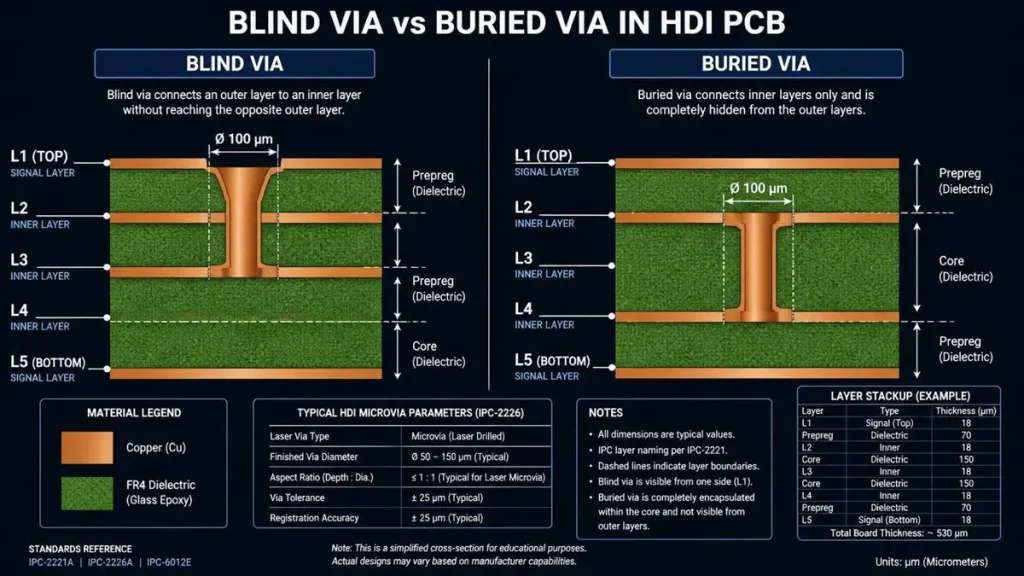
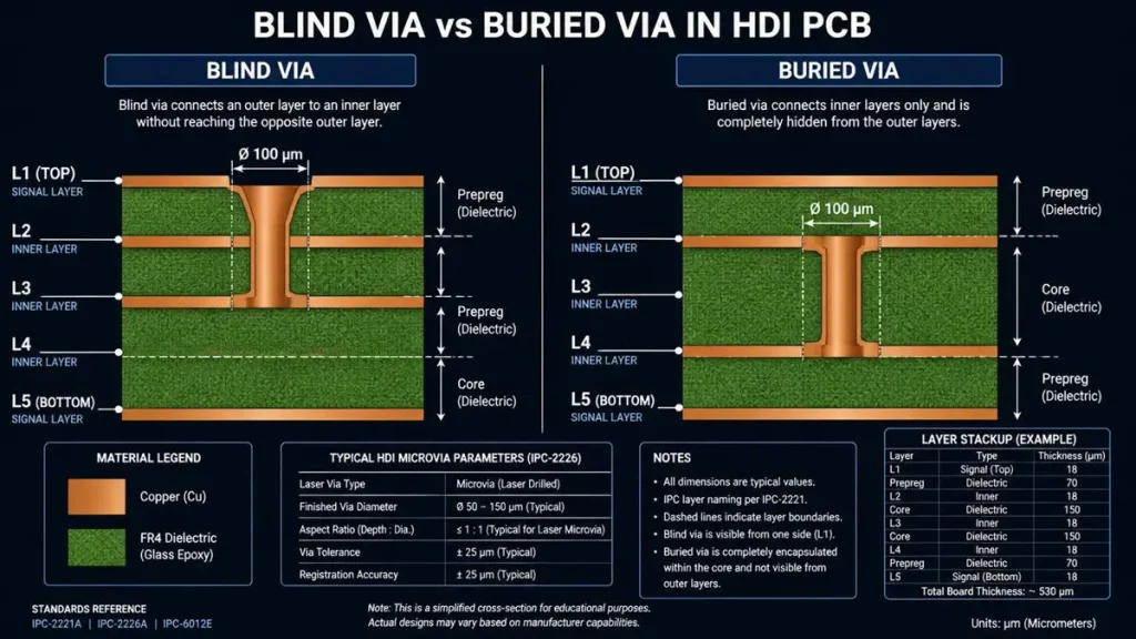
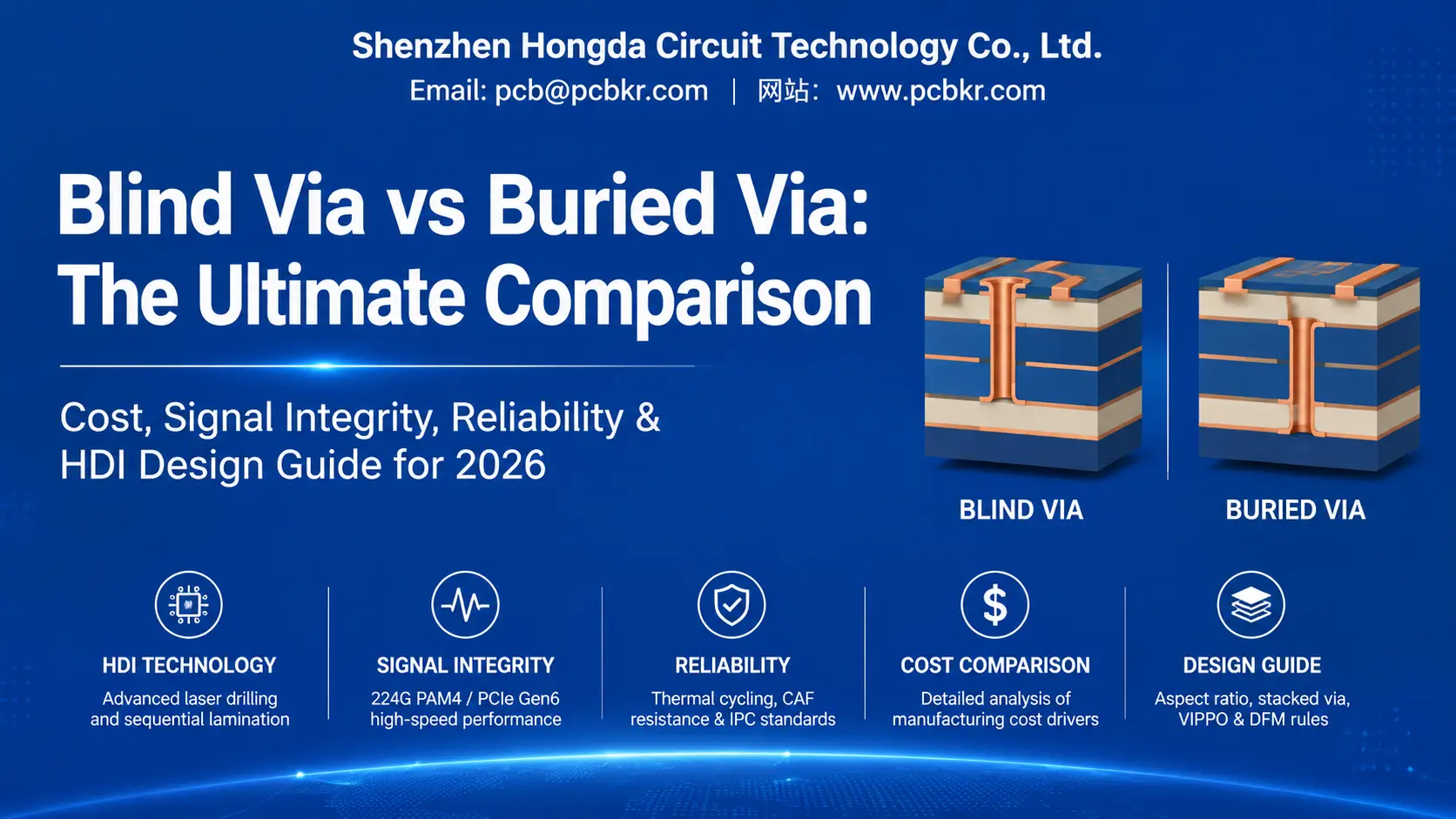
Blind Via vs. Buried Via Structure Comparison in HDI PCB Manufacturing
A blind via is a plated hole that originates on one of the outer layers of a multilayer PCB and terminates at a specific inner layer without penetrating the entire board thickness. Unlike a through-hole via, which traverses all layers, a blind via creates a direct electrical path from the surface to an internal routing layer while preserving the opposite surface for component mounting or additional routing channels.
Structural Characteristics of Blind Vias
The physical structure of a blind via is defined by three critical parameters:
- Drill Diameter: In 2026 HDI production, laser-drilled blind vias range from 50 μm (UV laser) to 150 μm (CO₂ laser), with 75–100 μm being the most common specification for AI server motherboards.
- Aspect Ratio: The ratio of dielectric thickness to via diameter must remain at or below 1:1 for reliable electroless copper plating. For high-yield production, Hongda targets 0.8:1.
- Depth Control: The laser must stop precisely at the target copper layer. Modern UV/CO₂ hybrid systems use real-time energy compensation and CCD vision alignment to maintain depth tolerance within ±10 μm across the full panel.
Why HDI Designs Prefer Blind Vias
Blind vias solve the fundamental space constraint of high-density interconnect (HDI) boards. By connecting Layer 1 directly to Layer 3 (a “1-3” blind via), designers eliminate the need to route signals through intermediate layers, freeing those layers for power distribution or additional signal paths. This is particularly critical beneath fine-pitch BGA devices where escape routing density determines whether a design is manufacturable at all.
In 2026, the shift toward Any-Layer HDI—where every layer transition uses laser-drilled microvias—has made blind via technology the default interconnect method for smartphones, AI accelerators, and 800G optical modules. The elimination of through-hole stubs also improves signal integrity at frequencies above 28 GHz, a requirement for 224G PAM4 and PCIe Gen6 channels.
Blind Via Applications in 2026
- AI Server PCBs: GPU substrate routing, NVLink 5.0 signal paths, HBM memory interfaces
- 5G/6G Base Stations: Millimeter-wave antenna feed networks requiring minimal via stub
- Automotive ADAS: Radar module PCBs with 77 GHz RF front-ends
- Medical Imaging: Compact ultrasound and endoscope controller boards
What Is a Buried Via? Internal Layer Connection & Manufacturing
A buried via is a plated hole that connects two or more internal layers of a multilayer PCB without reaching either outer surface. Because it is completely encapsulated within the board stackup, a buried via is invisible on the finished product and consumes zero surface real estate.
How Buried Vias Differ from Blind Vias
| Feature | Blind Via | Buried Via |
|---|---|---|
| Layer Connection | Outer ↔ Inner | Inner ↔ Inner |
| Surface Visibility | Yes (one side) | No (fully hidden) |
| Typical Drill Method | UV/CO₂ Laser | Mechanical or Laser |
| Lamination Cycle | Added during build-up | Formed in core before outer lamination |
| Repair Accessibility | Difficult | Almost impossible |
Buried Via Manufacturing: The Core-First Approach
Buried vias are fabricated during the inner layer core processing stage, before the outer layers are laminated. The typical workflow is:
- Core Drilling: Mechanical drills (typically 0.15–0.30 mm) or CO₂ lasers create holes in the inner layer core.
- Electroless Copper Plating: The drilled core receives a thin copper seed layer.
- Pattern Etching: Circuit traces are formed on the core surfaces.
- Core Lamination: The processed core is sandwiched between prepreg and additional copper foils.
- Sequential Build-Up: Outer layers and blind vias are added in subsequent lamination cycles.
Because buried vias are sealed inside the board, they cannot be inspected by surface AOI or probed after final lamination. This drives the requirement for 100% cross-section verification at the core level and X-ray inspection of the finished panel to confirm layer-to-layer registration.
Advantations of Buried Vias in Multilayer Designs
- Surface Preservation: Every buried via frees surface pads for component placement, critical in BGA-dense designs.
- Shorter Signal Paths: Internal power/ground plane connections via buried vias reduce loop inductance compared to through-hole alternatives.
- EMI Reduction: Hidden vias do not act as unintended antennas radiating from the board surface.
- Structural Integrity: In high-layer-count boards (20+ layers), buried vias distribute interconnection load across the stackup without creating surface stress concentration points.
Limitations of Buried Vias
- No Post-Fabrication Access: Once laminated, a defective buried via cannot be repaired; the entire panel is scrap.
- Higher Sequential Lamination Count: Each buried via layer pair may require an additional lamination cycle, increasing cost and lead time.
- Inspection Complexity: X-ray and microsection analysis are mandatory, adding quality assurance overhead.
- Design Inflexibility: Buried via layer pairs must be defined at the design stage and cannot be modified without a full board respin.
Blind Via vs Buried Via: Complete Comparison Table
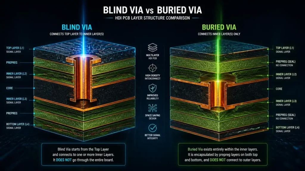
3D Cross-Section: Blind Via vs. Buried Via Layer Structure in HDI PCB
The following table provides a side-by-side technical evaluation for procurement engineers and PCB designers evaluating blind via PCB vs buried via PCB options for 2026 HDI projects.
| Comparison Item | Blind Via | Buried Via |
|---|---|---|
| Connection Layers | Outer ↔ One or more inner layers | Inner ↔ Inner only |
| Visible After PCB Finished | Yes (on starting surface) | No (fully encapsulated) |
| Primary Drill Technology | UV/CO₂ Hybrid Laser | Mechanical drill or CO₂ laser |
| Minimum Via Diameter (2026) | 50 μm (UV laser) | 100 μm (mechanical) |
| Aspect Ratio (Production) | ≤ 1:1 (target 0.8:1) | ≤ 1:12 (mechanical) |
| Routing Density | Very High | High |
| Signal Integrity at 56 GHz | Excellent (stub eliminated) | Excellent (no surface discontinuity) |
| Stub Reduction | Excellent (shallow depth) | N/A (no stub by design) |
| Sequential Lamination Required | Yes (1–6 cycles for HDI) | Yes (core + build-up cycles) |
| Manufacturing Difficulty | High | Very High |
| Relative Cost per Via | High | Higher (15–30% premium over blind) |
| Production Yield (Typical) | 85–92% | 78–88% |
| Inspection Method | AOI + X-ray + Cross-section | X-ray + Core-level microsection |
| Repairability | Difficult (requires milling) | Almost impossible |
| AI Server Suitability (224G) | Excellent (BGA escape) | Excellent (power plane routing) |
| Automotive (ADAS/Radar) | Excellent | Excellent |
| Aerospace (MIL-STD) | Excellent | Excellent (reduced EMI) |
| Medical Device Miniaturization | Excellent | Good (limited by core thickness) |
Note: Yield figures represent typical industry ranges for 6+N+6 HDI structures. Hongda’s qualified processes achieve 93%+ first-pass yield on 4+N+4 blind via designs and 87%+ on buried via core assemblies through automated optical alignment and real-time drill parameter feedback.
Blind Via Manufacturing Process vs Buried Via Manufacturing Process
Understanding the fabrication workflow is essential for procurement teams evaluating blind via PCB manufacturers and buried via PCB manufacturers. The processes diverge at the lamination stage.
Blind Via Manufacturing Process at Shenzhen Hongda Circuit Technology Co., Ltd.
Step 1: UV/CO₂ Hybrid Laser Drilling Hongda operates 12 CO₂ laser drill systems and 6 UV laser drill systems. The hybrid process uses UV laser (355 nm) to ablate the copper foil opening, followed by CO₂ laser (9.4 μm) to remove dielectric material. For 50 μm microvias in Any-Layer HDI, UV laser performs both copper and dielectric ablation in a single beam path. Multi-pulse drilling strategies prevent copper overburn at the via bottom while maintaining hole wall smoothness (Ra < 0.5 μm).
Step 2: Plasma Desmear & Chemical Cleaning After laser drilling, panels undergo plasma desmear using tetrafluoromethane/oxygen chemistry. This dry process removes resin smear from microvia walls without attacking copper, a critical advantage over wet chemical desmear for vias under 100 μm where fluid penetration is unreliable.
Step 3: Electroless Copper Deposition A palladium-activated electroless copper process deposits 0.8–1.2 μm of copper on via walls. Hongda’s automated horizontal plating line maintains bath chemistry within ±2% of target concentration, ensuring uniform coverage even at 1:1 aspect ratios.
Step 4: Electrolytic Copper Plating & Via Filling For via-in-pad (VIPPO) applications, blind vias are filled with electrolytic copper to achieve <5% void rate per IPC-4761 Type VII. The filled via is then planarized and capped with 8–12 μm of copper. For non-VIPPO designs, standard through-plating achieves 20 μm minimum barrel copper.
Step 5: Sequential Lamination Each lamination cycle bonds a new dielectric and copper foil pair to the existing sub-composite. Hongda’s Lauffer vacuum lamination press controls temperature ramp at ±1°C and pressure uniformity within 3% across a 24×18 inch panel, preventing resin starvation and void formation in high-layer builds.
Step 6: AOI, X-Ray & Electrical Test Automated optical inspection (AOI) verifies trace geometry. X-ray inspection confirms blind via alignment and fill quality. Flying probe and grid-based electrical testing validate netlist continuity and isolation.
Buried Via Manufacturing Process
Step 1: Core Drilling & Plating The process begins with raw core material (typically 0.2–0.4 mm thick). Mechanical drills or CO₂ lasers create buried via holes. The core is then electroless and electrolytically plated to form the via barrel.
Step 2: Inner Layer Patterning Circuit traces are etched on both sides of the plated core. Buried via capture pads must be precisely aligned to ensure subsequent layers make proper electrical contact.
Step 3: Core Lamination & Registration The processed core is laminated between prepreg sheets and outer copper foils. Registration accuracy is critical: Hongda uses X-ray pre-alignment and automatic optical registration (AOR) to maintain layer-to-layer positional tolerance within ±25 μm.
Step 4: Outer Layer Build-Up Once the core is sealed, standard HDI build-up processes (laser drilling, plating, lamination) add outer layers and blind vias. The buried vias are now inaccessible for direct inspection.
Step 5: Destructive Verification Panel edge coupons are microsectioned to verify buried via barrel quality, copper thickness, and dielectric integrity. This is a destructive test; the coupon area is scrapped.
Blind Via vs Buried Via Cost Comparison for Procurement
Cost is often the decisive factor when procurement teams evaluate blind via PCB fabrication versus buried via PCB fabrication. While neither technology is inexpensive, understanding the cost drivers enables accurate budget forecasting.
Cost Drivers for Blind Via PCB Fabrication
- Laser Drilling Equipment Amortization: UV laser systems represent a capital investment of $800K–$1.2M per unit. This cost is distributed across panel volume.
- Sequential Lamination Cycles: Each additional lamination cycle adds 8–12 hours of press time and consumes prepreg material. A 2+N+2 HDI requires two lamination cycles; 6+N+6 requires six.
- Yield Loss: Blind vias in high-aspect-ratio stacks have a higher risk of plating voids or misregistration. Typical yield loss accounts for 5–8% of panel cost.
- Inspection Overhead: 100% AOI and sample cross-section analysis add labor and equipment time.
- Material Selection: Low-loss laminates (Megtron 6/7, Tachyon 100G) required for 224G PAM4 designs cost 3–5× standard FR4.
Cost Drivers for Buried Via PCB Fabrication
- Core Processing Complexity: Buried vias require dedicated core drilling and plating lines, often with slower throughput than surface processing.
- Higher Scrap Risk: A defect in a buried via is only detectable after full lamination, at which point the entire panel (including all outer layer work) is lost. This drives a risk premium in pricing.
- Additional Lamination Steps: Buried via cores often require their own lamination cycle before outer layer build-up, adding 20–30% to total lamination time.
- X-Ray Inspection Capital: High-resolution X-ray systems for buried via verification cost $300K–$500K and require skilled operators.
Relative Cost Positioning (2026 Estimates)
| PCB Type | Relative Cost Index | Notes |
|---|---|---|
| Standard Through-Hole (8L) | 1.0× | Baseline |
| Blind Via Only (1+N+1, 8L) | 1.8–2.2× | Single lamination cycle |
| Blind Via HDI (2+N+2, 12L) | 2.5–3.5× | Two lamination cycles |
| Buried Via + Blind Via (4+N+4, 16L) | 3.5–5.0× | Core + multiple build-ups |
| Any-Layer HDI (Stacked Microvias) | 4.0–6.5× | Maximum complexity |
These indices are representative for medium-volume production (100–500 panels). High-volume orders (5,000+ panels) achieve 15–25% cost reduction through tooling amortization and process optimization.
Which Via Provides Better Signal Integrity? 224G PAM4 & PCIe Gen6 Analysis
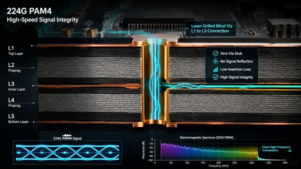
3D cross-section analysis of a laser-drilled blind via (L1 to L3) optimizing 224G PAM4 signal integrity by eliminating via stubs and insertion loss.
Signal integrity (SI) is the dominant engineering concern for 2026 high-speed PCB designs. At 224G PAM4 (56 GHz Nyquist) and PCIe Gen6 (64 GT/s), via transitions are no longer negligible discontinuities—they are primary channel budget consumers.
The Via Stub Problem
A via stub is the unused portion of a plated hole extending beyond the signal layer. In a through-hole via on a 32-layer board, the stub might be 60 mil (1.5 mm) long. At 56 GHz, this stub acts as a quarter-wave resonator, creating an insertion loss notch at approximately 15 GHz and its third harmonic at 45 GHz—directly inside the 224G signaling band.
The math is unforgiving: A 50-mil stub can introduce a 6–10 dB insertion loss notch that no amount of receiver equalization can recover. For PCIe Gen6, stub length must be controlled to <10 mil (ideally <5 mil) to push resonance above 80 GHz.
Why Blind Vias Excel at High Speed
Blind vias inherently eliminate the stub because they terminate at the target layer. A laser-drilled blind via connecting Layer 1 to Layer 3 has zero stub on either end. This makes blind vias the preferred solution for:
- BGA Escape Routing: Fine-pitch devices (0.35–0.4 mm pitch) require via-in-pad with 8–10 mil drill sizes. Only laser-drilled blind vias achieve this geometry.
- Layer Transition in Stripline: 224G channels must route on internal stripline layers. Blind vias provide the shortest path from surface BGA pads to inner routing layers.
- Controlled Impedance: With anti-pad optimization, blind via impedance can be matched to 85 Ω ±5% differential, maintaining continuity through the transition.
Buried Vias and Signal Integrity
Buried vias do not create stubs because they never reach the surface. However, they introduce a different challenge: layer-to-layer crosstalk. In dense buried via fields beneath BGA arrays, adjacent signal vias can couple capacitively. Proper ground via stitching (four ground vias per differential pair, placed within 12 mil) mitigates this effect.
For pure internal routing—such as power plane stitching or mid-board layer transitions—buried vias offer SI performance equal to blind vias with the added benefit of surface pad preservation.
2026 High-Speed Design Recommendations
| Application | Recommended Via Strategy | Rationale |
|---|---|---|
| 224G PAM4 (AI Server) | Blind via + back-drilled through-hole | Eliminates stub; VIPPO for BGA escape |
| PCIe Gen6 (64 GT/s) | Blind via preferred; buried via for internal planes | Stub <5 mil mandatory |
| 800G/1.6T Ethernet | Stacked blind microvias | Minimizes transition loss |
| CXL 3.0 | Blind via with ground via co-location | Controls mode conversion |
| Automotive Radar (77 GHz) | Buried via for RF feed networks | Reduces surface radiation |
Blind Via vs Buried Via Reliability: Thermal Cycling & CAF Resistance
Reliability in HDI PCBs is measured not by initial electrical test pass rates, but by performance after thermal cycling, humidity exposure, and long-term electrical stress. Both blind and buried vias face distinct failure modes.
Common Failure Modes in Blind Vias
- Via Void & Barrel Crack: Incomplete copper plating or excessive thermal expansion during reflow can create voids that propagate into cracks. Hongda’s electrolytic fill process achieves <5% void rate, verified by cross-section on every production lot.
- Resin Recession: In filled blind vias, differential CTE between copper fill and surrounding laminate can cause the fill to recess below the pad surface during thermal cycling. IPC-4761 Type VII fill with cap plating prevents this.
- Misregistration: Laser drill positional error >15 μm can cause the via to miss the capture pad, creating an open circuit. Hongda’s drill systems use panel fiducial alignment with ±8 μm repeatability.
- CAF (Conductive Anodic Filament): In high-humidity environments, electrochemical migration can create conductive filaments between biased vias. This is mitigated by using high-Tg, low-CAF laminates and maintaining minimum via-to-via spacing per IPC-2226.
Common Failure Modes in Buried Vias
- Core Delamination: Poor lamination pressure or moisture absorption in prepreg can cause separation at the buried via core interface. Vacuum lamination with controlled ramp rates eliminates voids at this critical boundary.
- Copper Fatigue: Buried via barrels experience shear stress during thermal cycling due to CTE mismatch between copper and FR4. High-Tg materials (Tg > 170°C) and annealed copper foils improve fatigue resistance.
- Inner Layer Misalignment: If the core shifts during lamination, the buried via may not connect properly to adjacent layer traces. X-ray inspection catches this before outer layer processing.
- Plating Non-Uniformity: Mechanical drilling of thick cores can create aspect ratios >10:1, making uniform plating difficult. Hongda limits mechanical buried via aspect ratio to 8:1; higher ratios use laser drilling.
Reliability Testing Standards
Hongda subjects all blind and buried via designs to:
- IST (Interconnect Stress Test): 6× thermal shock (-40°C to +150°C) with resistance monitoring
- TCT (Thermal Cycling Test): 1,000 cycles (-65°C to +150°C) per IPC-TM-650 2.6.7
- CAF Resistance: 85°C/85% RH, 100V DC bias for 1,000 hours
- Solder Float: 288°C for 10 seconds, 3× repetition
HDI PCB Design Rules: Aspect Ratio, Stacked Via & Via-in-Pad
Successful blind via and buried via implementation requires adherence to design for manufacturability (DFM) rules that balance electrical performance with fabrication yield.
Aspect Ratio Guidelines
| Via Type | Recommended Max Aspect Ratio | Absolute Max (Hongda) | Notes |
|---|---|---|---|
| Blind Via (Laser) | 0.8:1 | 1.0:1 | Depth = dielectric thickness |
| Blind Via (Mechanical) | 1.0:1 | 1.2:1 | Limited to larger diameters |
| Buried Via (Mechanical) | 8:1 | 10:1 | Core thickness / drill diameter |
| Buried Via (Laser) | 1.0:1 | 1.2:1 | For thin-core applications |
Capture Pad & Annular Ring
- Blind Via Capture Pad: Minimum annular ring of 50 μm (2 mil) for laser-drilled vias. For via-in-pad designs, the pad must accommodate both the via drill and the BGA ball landing zone.
- Buried Via Capture Pad: Minimum 75 μm annular ring to account for core lamination shift. Inner layer pads should be 0.1–0.15 mm larger than the drill diameter.
Stacked vs. Staggered Microvias
- Staggered Microvias: Offset between layer transitions. Preferred for reliability because stress is distributed. Minimum offset = 1× via diameter.
- Stacked Microvias: Directly aligned through multiple layers. Required for Any-Layer HDI but demands copper-filled lower vias to prevent barrel cracking. Hongda qualifies stacked microvias to 4 levels in production.
Via-in-Pad (VIPPO) Specifications
For 0.35 mm BGA pitch and finer:
- Drill diameter: 8–10 mil (200–250 μm)
- Fill material: Electrolytic copper (preferred) or conductive epoxy
- Dimple after fill: <10 μm
- Cap plating: 8–12 μm copper + ENIG or ENEPIG finish
- Void rate: <5% by cross-section area
IPC Standards for HDI Vias
- IPC-2226: Design standard for HDI and microvias
- IPC-6012: Qualification and performance specification for rigid PCBs (Class 2 for commercial, Class 3 for high-reliability)
- IPC-4761: Protection of printed board via structures (Type VII for filled and capped vias)
- IPC-TM-650: Test methods for thermal stress, CAF, and plating adhesion
Industry Application Comparison: AI Servers, Automotive & Aerospace
The choice between blind via and buried via is ultimately an application-specific optimization. Below is a decision matrix for key 2026 markets.
AI Server PCBs: Why Blind Vias Dominate
AI server motherboards and GPU substrates in 2026 routinely exceed 24 layers with BGA pitches down to 0.35 mm. The NVIDIA B200/GB300 generation requires:
- 224G PAM4 SerDes routing with <8 mil via stubs
- NVLink 5.0 and PCIe Gen6 channels
- HBM3e memory interfaces at 9.6 Gbps
Blind via adoption: Near-universal for BGA escape and layer transition. Buried vias are used for internal power distribution and ground plane stitching where surface access is unnecessary.
Networking Equipment: 800G/1.6T Optical Modules
Switch fabric cards and optical module PCBs demand:
- Line width/space below 2 mil (50 μm)
- Impedance control within ±3%
- Minimal insertion loss at 56 GHz
Blind via adoption: Laser-drilled microvias with stacked configurations for Any-Layer routing. Buried vias are rare in these thin, high-density designs.
Automotive Electronics: ADAS & EV Powertrains
Automotive PCBs must survive:
- -40°C to +150°C under-hood temperatures
- Vibration per ISO 16750-3
- 15-year operational life
Blind via adoption: Used in radar (77 GHz) and camera module PCBs for miniaturization. Buried vias are preferred in battery management systems (BMS) and motor controllers where high voltage isolation and EMI containment are critical.
Aerospace & Defense: MIL-STD-810 & DO-160
Aerospace PCBs prioritize reliability over density:
- 20–40 layer rigid boards
- High-Tg polyimide or ceramic-filled PTFE
- Class 3 manufacturing with full traceability
Buried via adoption: Extensive use for internal redundancy and radiation-hardened routing. Blind vias are used sparingly due to repair difficulty in deployed systems.
Medical Devices: Imaging & Implantables
Medical PCBs require:
- Biocompatible materials (where applicable)
- Extreme miniaturization for wearables
- High signal fidelity for imaging
Blind via adoption: Dominant in portable ultrasound and endoscope controllers. Buried vias are used in implantable devices where hermetic sealing and long-term reliability outweigh cost concerns.
Blind Via or Buried Via: Which One Should You Choose?
The following decision framework helps procurement and engineering teams select the optimal via strategy.
Decision Matrix
| If Your Design Requires… | Recommended Via Type | Rationale |
|---|---|---|
| Fine-pitch BGA escape (<0.4 mm pitch) | Blind Via | Only laser-drilled blind vias achieve required density |
| Surface component density maximization | Blind Via | Frees inner layers for routing |
| Pure internal layer interconnection | Buried Via | Preserves both surfaces for components |
| 224G PAM4 / PCIe Gen6 signal paths | Blind Via | Stub elimination mandatory |
| High-voltage isolation (EV/BMS) | Buried Via | Encapsulated structure prevents arcing |
| Cost-sensitive consumer electronics | Through-Hole | Blind/buried vias add 2–4× cost |
| Maximum density (smartphone, watch) | Blind + Buried + Microvia | Any-Layer HDI with stacked vias |
| Repairability in deployed systems | Through-Hole | Blind/buried vias are not field-repairable |
| EMI reduction in RF applications | Buried Via | No surface radiation from hidden vias |
When to Use a Hybrid Approach
The most advanced 2026 designs—AI server motherboards, 5G baseband units, and autonomous driving controllers—use all three via types in a single board:
- Through-hole vias for mechanical mounting and low-speed signals
- Blind vias for high-speed BGA escape and layer transition
- Buried vias for internal power distribution and ground stitching
This hybrid approach optimizes cost, density, and performance but requires a manufacturer with demonstrated capability in sequential lamination, laser drilling, and high-layer-count registration.
Why Choose Shenzhen Hongda Circuit Technology Co., Ltd. as Your Blind Via PCB Manufacturer
Shenzhen Hongda Circuit Technology Co., Ltd. has invested continuously in HDI manufacturing capability to meet the demands of 2026’s most challenging PCB applications. Our facility is structured around three core competencies: precision imaging, controlled-depth laser processing, and high-layer sequential lamination.
Advanced Manufacturing Equipment
Precision Pattern Transfer
- SCREEN Ledia LDI Exposure System: Laser Direct Imaging eliminates phototool variability, achieving 20 μm line/space resolution with ±3 μm registration accuracy. Critical for 224G PAM4 differential pair routing where impedance tolerance must be held within ±5%.
Laser Microvia Machining
- Mitsubishi Electric UV/CO₂ Hybrid Laser Drilling: 12 CO₂ stations (75 μm minimum) and 6 UV stations (50 μm minimum) enable blind via diameters from 50–150 μm. Real-time energy compensation and CCD alignment maintain depth control within ±10 μm across 24×18 inch panels.
High-Performance Lamination
- Lauffer Vacuum Lamination Press: Multi-zone temperature control (±1°C) and programmable pressure profiling prevent delamination in 20–40 layer builds using low-loss materials like Megtron 6/7 and Rogers RO4000 series.
Automated Electroplating
- HX Automation PCB Plating Line: Continuous monitoring of copper sulfate concentration, acid normality, and additive levels ensures 20 μm minimum barrel copper in high-aspect-ratio vias and <5% void rate in filled blind vias.
Quality Assurance
- 3D AOI + X-Ray Inspection: Automated optical inspection verifies trace geometry to 1 μm precision. X-ray systems confirm blind/buried via alignment and detect voids non-destructively.
- Flying Probe & Grid Electrical Test: 100% netlist verification for prototypes; grid testing for volume production.
Material Qualifications
Hongda maintains approved supplier programs for:
- Standard FR-4: High-Tg (170°C), mid-Tg (150°C)
- Low-Loss Laminates: Panasonic Megtron 6/7, Isola Tachyon 100G, Astra MT77
- High-Frequency Materials: Rogers RO4350B, RO4003C, Taconic TLY-5
- High-Tg / Low-CAF: For automotive and aerospace applications
- Polyimide: For flex-rigid and high-temperature designs
HDI Capability Range
| HDI Type | Layer Count | Microvia Size | Lamination Cycles | Applications |
|---|---|---|---|---|
| 1+N+1 | 4–12 layers | 100 μm | 1 | Consumer, industrial |
| 2+N+2 | 6–16 layers | 75 μm | 2 | Automotive, medical |
| 4+N+4 | 10–24 layers | 75 μm | 4 | Networking, AI edge |
| 6+N+6 | 16–32 layers | 50–75 μm | 6 | AI server GPU substrate |
| Any-Layer | 8–28 layers | 50 μm | 6+ | Smartphone, wearable |
Certifications & Standards
- IPC Class 2 / Class 3 manufacturing
- ISO 9001:2015 Quality Management
- ISO 14001:2015 Environmental Management
- IATF 16949:2016 Automotive Quality (in progress)
- UL 94V-0 flame rating
- RoHS 2.0 / REACH compliance
From Prototype to Volume
- Fast-Turn Prototype: 48-hour turnaround for 12-layer standard HDI; 5-day for 24-layer AI server builds with full impedance reporting.
- Volume Production: Automated lines support 10,000+ panel monthly output for blind/buried via HDI boards.
- Engineering Support: Dedicated DFM review team provides stackup simulation, impedance modeling, and via feasibility analysis before fabrication.
FAQ: Blind Via vs Buried Via PCB
What is the difference between a blind via and a buried via?
A blind via connects an outer layer to one or more inner layers and is visible from the board surface. A buried via connects only internal layers and is completely hidden within the PCB stackup. Blind vias are typically laser-drilled for HDI applications, while buried vias are formed in core material during sequential lamination.
Which via type is better for HDI PCBs: blind via or buried via?
Neither is universally superior. Blind vias are better for surface-to-inner routing, BGA escape, and high-speed signal paths where stub elimination is critical. Buried vias are better for internal layer interconnection, surface preservation, and EMI-sensitive applications. Most advanced HDI designs use both.
Are blind vias more expensive than buried vias?
Buried vias are generally 15–30% more expensive than blind vias due to additional core processing, higher scrap risk, and more complex inspection requirements. However, the total board cost depends on layer count, lamination cycles, and material selection. A simple 1+N+1 blind via board may cost less than a buried via design, but a 6+N+6 Any-Layer HDI with stacked blind vias will exceed the cost of most buried via implementations.
Can blind vias improve signal integrity for 224G PAM4 and PCIe Gen6?
Yes. Blind vias eliminate via stubs, which are the primary source of insertion loss notches at 56 GHz (224G PAM4 Nyquist). For PCIe Gen6, blind vias with <5 mil effective stub length are strongly preferred over back-drilled through-hole vias. Hongda’s laser-drilled blind vias achieve this with zero residual stub when properly designed.
How do I choose a reliable blind via and buried via PCB manufacturer?
When evaluating a blind via PCB manufacturer or buried via PCB manufacturer, verify the following capabilities:
Laser drilling equipment: Do they operate UV and CO₂ hybrid systems? What is their minimum microvia diameter (50 μm is the 2026 standard for Any-Layer HDI)?
Sequential lamination capacity: How many lamination cycles can they support? 6+N+6 requires six cycles with precise registration.
Via fill capability: Can they achieve IPC-4761 Type VII copper fill with <5% voids?
Inspection infrastructure: Do they have 3D AOI, X-ray, and cross-section capability for both blind and buried vias?
Material qualifications: Are Megtron 6/7, Tachyon 100G, and Rogers materials in their approved vendor list?
High-speed design experience: Have they shipped 224G PAM4 or PCIe Gen6 boards with documented SI performance?
Certifications: IPC Class 3, ISO 9001, and automotive certifications (IATF 16949) indicate process maturity.
Shenzhen Hongda Circuit Technology Co., Ltd. meets all of these criteria and provides documented DFM reviews, impedance coupons, and first-article inspection reports with every HDI order.
© 2026 Shenzhen Hongda Circuit Technology Co., Ltd. All rights reserved. For technical inquiries or quotation requests, contact our engineering team at pcb@pcbkr.com.
About Author
David Chen https://www.linkedin.com/in/pcbcoming
David Chen boasts an extensive professional background in PCBA manufacturing, PCBA testing, and PCBA optimization, with specialized expertise in high-precision PCBA fault analysis and rigorous PCBA reliability testing. The author has worked with high-layer-count server PCB fabrication, ultra-low-loss backplane stackups, and thermo-mechanical reliability optimization for AI infrastructure projects involving 112G and 224G PAM4 architectures. Skilled in complex circuit design and cutting-edge advanced PCB manufacturing processes, he delivers solutions that elevate product durability and performance across industrial applications. His technical articles focusing on PCBA manufacturing workflows and testing methodologies are widely cited by industry peers, research institutions, and technical platforms, solidifying his reputation as a recognized technical authority in the global circuit board manufacturing sector.