High Reliability Multilayer Immersion Gold PCBs: A Procurement Engineer’s Guide to Material Selection, Manufacturing Tolerances, and Supplier Vetting
Executive Summary: Why Immersion Gold PCB Procurement Decisions Matter More
The global PCB ENIG chemical market has crossed USD 3.5 billion in China alone and is accelerating toward USD 5.0 billion by 2033 at a 6.2% CAGR, driven by 5G infrastructure, electric vehicles, and AI server hardware demanding sub-micron plating precision.
For procurement leads and hardware engineers sourcing multilayer immersion gold PCBs, the stakes have never been higher: a single black pad defect or CTE mismatch in an Arlon stackup can cascade into field failures costing six figures in aerospace or medical deployments.
This guide moves beyond generic surface finish comparisons. We dissect the 6-layer and 8-layer Arlon immersion gold PCB stackup architectures that Western OEMs now specify for mission-critical RF, aerospace, and high-density server applications. We map the ENIG vs hard gold selective plating decision tree—when to spec immersion gold for SMT pads, when to mandate electroplated hard gold for edge connectors, and how to prevent gold embrittlement at the boundary. Finally, we benchmark what a capable immersion gold PCB manufacturer must deliver in 2026, from mSAP-compatible ENIG lines to IPC-6012 Class 3 XRF traceability, using the production reality at Shenzhen Hongda Circuit Technology Co., Ltd. as a reference standard.
Section 1: Material Physics and Why Arlon Substrates Dominate High-Frequency Immersion Gold PCBs
1.1 The Thermal-Electrical Performance Gap: Arlon vs. Standard FR-4
When your design pushes beyond 10 GHz—whether in phased-array radar, 112G PAM4 backplanes, or mmWave 5G base stations—standard FR-4 laminates become liabilities. Arlon polyimide and PTFE-based substrates (85N, 33N, 55NT) deliver dielectric constants (Dk) between 2.4 and 3.0 and loss tangents (Df) below 0.003, compared to FR-4’s Dk of ~4.7 and Df of 0.022. More critically, Arlon’s Z-axis CTE stays under 1.2% across the -55°C to +125°C thermal shock range, virtually eliminating via wall cracking and microvia stress that plague high-layer-count FR-4 builds during thermal cycling.
For procurement teams, this translates to a simple rule: if the BoM specifies high frequency PCB surface finish requirements above 6 GHz, the substrate conversation must start with Arlon or equivalent Rogers/Taconic materials, not FR-4 hybrids.
1.2 CTE Matching and the ENIG Adhesion Challenge on PTFE/Polyimide
Here is where most fabricators fail. PTFE and polyimide surfaces are chemically inert. Without proper pre-treatment, the electroless nickel layer in an ENIG stack achieves adhesion strength well below the 1.0 N/mm threshold required for IPC-6012 Class 3 reliability. The fix is a dual-stage surface activation: plasma etching to create micro-roughness at the nanometer scale, followed by chemical micro-etching to expose reactive sites for nickel nucleation.
At Shenzhen Hongda Circuit Technology, this process is non-negotiable for all Arlon-based immersion gold orders. The company’s 2026 equipment upgrade includes plasma treatment stations integrated directly into the ENIG line, ensuring nickel peel strength exceeds 1.2 N/mm on PTFE cores—critical for boards that will see 1,000+ thermal cycles in aerospace enclosures.
1.3 Dielectric Stability Under Reflow: Why Tg >250°C Matters
Immersion gold PCBs see multiple thermal shocks: ENIG bath exposure (~80°C), solder mask cure (~150°C), and final assembly reflow (peak 245–260°C). Arlon substrates with glass transition temperatures above 250°C maintain dimensional stability through this cascade, preventing the pad cratering and resin recession that create latent solder joint defects. For procurement engineers evaluating high reliability PCB quotes, always verify the substrate Tg against your peak assembly profile—not just the operating temperature.
Section 2: 6-Layer Arlon Immersion Gold PCB Stackup Design and Manufacturing Rules
2.1 Preferred 6-Layer Stackup for RF and Mixed-Signal Applications
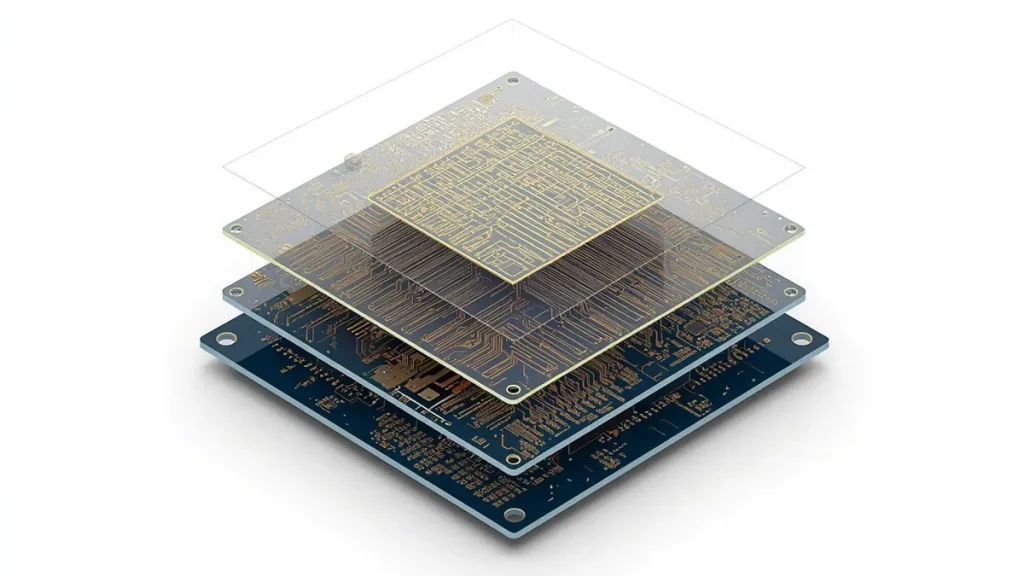
3D Exploded Stackup Architecture of 6-Layer High-Frequency Arlon Immersion Gold (ENIG) PCB
The following stackup has become the de facto standard for procurement teams sourcing 6 layer Arlon immersion gold PCB builds for aerospace transceivers and medical imaging front-ends:
| Layer | Function | Copper Weight | Material | Dielectric Thickness |
|---|---|---|---|---|
| L1 (Top) | Signal / High-Speed RF | 1 oz + ENIG | Arlon Core / Foil | 3.5 mil |
| L2 | Ground Plane | 1 oz | Arlon Prepreg | 4.0 mil |
| L3 | Signal Layer 2 | 0.5 oz | Arlon Core | 8.0 mil |
| L4 | Power Plane | 1 oz | Arlon Prepreg | 8.0 mil |
| L5 | Ground Plane | 1 oz | Arlon Core | 4.0 mil |
| L6 (Bottom) | Signal / Component | 1 oz + ENIG | Arlon Prepreg / Foil | 3.5 mil |
Procurement note: The 0.5 oz inner signal layer (L3) is intentional. Thinner copper reduces etch undercut, enabling 3.5 mil trace/space geometries on Arlon’s low-Dk core without impedance drift. When issuing an RFQ, specify whether your fabricator can hold ±5% differential impedance control on this stackup—Shenzhen Hongda Circuit Technology validates this spec using polar TDR measurement on every panel, not just first-article inspection.
2.2 Microvia Processing: Laser Drilling and Desmear Protocols
Blind and buried microvias in Arlon layers demand CO₂/UV laser drilling with pulse energy tuned to the substrate’s resin chemistry. The debris left in PTFE microvias cannot be cleaned with standard alkaline permanganate desmear; it requires plasma desmear using CF₄/O₂ chemistry to fluorinate and volatilize PTFE residue. Any fabricator quoting your multilayer immersion gold PCB project without plasma desmear capability on the traveler should be disqualified for Arlon builds.
2.3 Black Pad Prevention: The Phosphorus Content Control Window
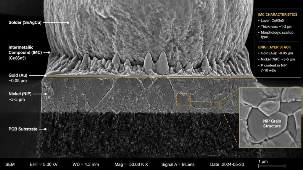
SEM Cross-Section of BGA Solder Joint on ENIG Pad Showing 7–10 wt% Phosphorus Ni-P Grain Structure and IMC Layer
Black pad—the brittle nickel corrosion layer that destroys BGA solder joints—remains the single most common ENIG field failure mode. Prevention hinges on maintaining electroless nickel phosphorus content in the 7–10% mid-phosphorus band and hyper-corrosion inhibitors in the immersion gold bath. Procurement engineers should require XRF thickness mapping (nickel 120–240 µin, gold 1.2–3.0 µin) and SEM cross-section validation of the Ni-P grain structure on first articles. Shenzhen Hongda Circuit Technology runs automated XRF on 100% of ENIG panels, with batch records tied to individual work orders for full IPC-2581 traceability.
Section 3: 8-Layer Immersion Gold PCB Stackup and Controlled Impedance Architecture
3.1 Symmetrical Construction to Eliminate Board Warp
For 8 layer immersion gold PCB designs—common in software-defined radio, AI inference accelerators, and military compute modules—symmetry is non-negotiable. The standard balanced stackup follows an S1-G1-S2-P1-G2-S3-G3-S4 arrangement, with mirror-image dielectric thicknesses above and below the central power plane. This geometry keeps warp and twist within IPC-6012 Class 3 tolerances (<0.5%) after ENIG processing and multiple reflow cycles.
Procurement tip: Asymmetric stackups (e.g., placing all signal layers on the top half) may save a few dollars in prepreg material but will warp during the ENIG bath’s thermal excursion, destroying BGA planarity. Reject any DFM proposal that sacrifices symmetry for cost.
3.2 Skin Effect Management at 10 GHz and Beyond
At microwave frequencies, current concentrates at the conductor surface. The ENIG nickel underlayer (µ ~1.0–1.5 µΩ·cm) contributes resistive loss that becomes measurable above 10 GHz. For RF microwave PCB manufacturing targeting Ka-band or 224G PAM4 signaling, specify:
- Surface roughness Rq < 0.5 µm on signal layers (achieved via ultra-low-profile copper foil)
- Nickel thickness at the lower end of the IPC-4552 window (120–150 µin) to minimize skin depth penetration
- Gold thickness 2.0–3.0 µin to ensure pore-free coverage without excessive IMC formation
Shenzhen Hongda Circuit Technology addresses this by offering selective ENIG on RF signal pads with optimized nickel thickness, while routing lower-frequency digital nets through standard ENIG parameters—a hybrid approach that cuts insertion loss by 8–12% on 28 GHz differential pairs compared to uniform-thickness ENIG.
3.3 Thermal Dissipation and Copper Thieving for Uniform Plating
Dense BGA arrays create current density crowding during electroless nickel deposition, resulting in thicker nickel at array edges and thinner centers. Automated copper thieving pattern placement around the BGA periphery equalizes current distribution, ensuring ENIG thickness uniformity within ±10% across the entire array. For thermal management, specify 0.3 mm plated through-hole via arrays under thermal pads, tied to internal ground planes with direct copper connections. This bypasses the thermal resistance of the Arlon core, which—while electrically excellent—is thermally insulative compared to metal-core alternatives.
Section 4: Hybrid Surface Finishing—ENIG Plus Selective Hard Gold Plating
4.1 The Functional Separation: When to Spec Which Gold Finish
Immersion gold and hard gold serve fundamentally different roles on the same PCB. Procurement engineers frequently conflate them, leading to either premature connector wear or solder joint embrittlement. Here is the 2026 decision matrix:
| Attribute | Immersion Gold (ENIG) | Hard Gold Plating (Electroplated) |
|---|---|---|
| Gold Thickness | 1.2–3.0 µin (0.03–0.08 µm) | 15–50 µin (0.38–1.27 µm) |
| Primary Function | SMT solderability, BGA planarity | Edge connectors, gold fingers, wear surfaces |
| Wear Cycles | <20 insertion cycles | >2,000 insertion/mating cycles |
| Solderability | Excellent (gold dissolves into solder) | Poor (risk of gold embrittlement if >5% by vol) |
| Process Position | After solder mask | Before solder mask |
Rule of thumb: If a pad will see a soldering iron or reflow oven, it gets ENIG. If it will see a connector insertion force, it gets hard gold. Never electroplate hard gold onto SMT pads— the cobalt/nickel alloying that gives hard gold its 130–200 HV hardness also makes it solder-resistant and prone to brittle intermetallic formation.
4.2 Dual-Process Workflow at the Manufacturing Floor
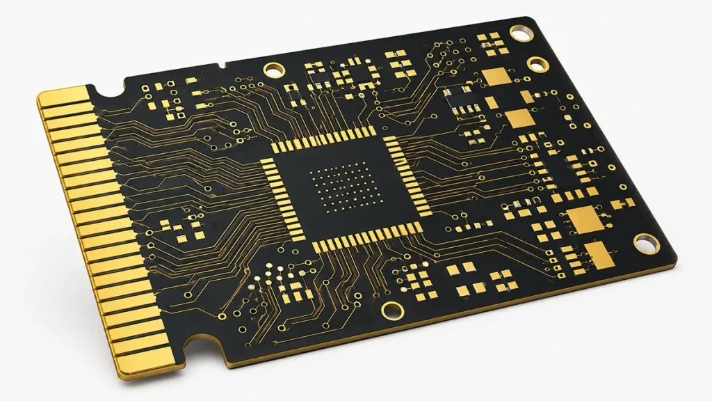
Hybrid Surface Finishing Layout: Selective Electroplated Hard Gold Edge Connectors and ENIG SMT Pads on Bare PCB
A true hybrid ENIG/hard gold PCB requires sequential masking:
- Primary copper etching and outer layer patterning
- Dry-film selective masking for edge fingers and high-wear contact zones
- Electroplating hard nickel/gold (cobalt-alloyed, 15–30 µin Au over 100–200 µin Ni)
- Mask stripping and LPI solder mask application
- Chemical ENIG line deposition for all remaining SMT pads and fine-pitch components
The critical procurement checkpoint is boundary clearance. Hard gold fingers must maintain >15 mil clearance from adjacent ENIG SMT pads. Any bridging between the two gold chemistries during mask registration creates a contamination path where hard gold alloy contaminates the ENIG bath, destroying solderability across the entire panel.
4.3 Gold Embrittlement Mitigation: The 5% Weight Threshold
Gold embrittlement occurs when gold concentration in a solder joint exceeds 5% by weight, forming continuous AuSn₄ intermetallic layers that fracture under mechanical shock.
With ENIG’s 1.2–3.0 µin gold layer, the gold fully dissolves and disperses during reflow, staying well below the embrittlement threshold. Hard gold at 15–50 µin does not. This is why hard gold areas must never be soldered—only pressed or slid into mating connectors.
For mixed-technology boards where a component lead accidentally bridges a hard gold trace, specify Ni₃Sn₄ IMC control through reflow profile optimization: peak temperature 235–245°C, time above liquidus <60 seconds, and rapid cooling to lock nickel at the interface before gold diffusion accelerates.
Section 5: DFM, Quality Inspection, and Procurement Compliance Checklist
5.1 Design for Manufacturability: Arlon-Specific Rules
Before releasing Gerbers, verify these parameters against your fabricator’s capability deck:
- Min trace/space on Arlon layers: 3.5/3.5 mil (laser-direct-imaging required; contact lithography cannot hold this on PTFE)
- Annular ring (external): >2 mil for IPC-6012 Class 3
- Microvia aspect ratio: ≤0.75:1 for reliable plating in Arlon prepreg
- Solder mask clearance: 2 mil over ENIG pads to prevent mask fracture during thermal cycling
- File output: Gerber RS-274X + drill tables + IPC-2581 stackup drawing with material callouts
5.2 Quality Assurance: Standards That Separate Tier-1 from Commodity Suppliers
| Test | Requirement | Why It Matters for Procurement |
|---|---|---|
| IPC-6012 Class 3/3A | Spaceflight and military acceptance criteria | Defines microsection, cleanliness, and thermal stress baselines |
| XRF Thickness Mapping | Nondestructive Ni/Au measurement per IPC-4552 | Verifies ENIG bath consistency without destroying panels |
| Thermal Stress Float | 288°C, 10 seconds, 3 cycles minimum | Simulates multiple reflow passes and rework cycles |
| 3D X-Ray (AXI) | 100% inspection on high-layer-count builds | Catches voids in BGA thermal vias and inner-layer misregistration |
| TDR Impedance | ±5% on all controlled impedance nets | Ensures signal integrity compliance before assembly |
Shenzhen Hongda Circuit Technology maintains IPC Class 3, ISO 13485 medical, and AS9100 aerospace certifications, with 100% 3D X-Ray inspection integrated into the workflow for all multilayer builds above 12 layers.
For procurement leads in regulated industries, this certification stack eliminates the audit burden of qualifying an uncertified Asian supplier.
5.3 The 2026 Procurement Decision Matrix: Cost vs. Risk
| Architecture | Best For | Cost Index | Risk Profile |
|---|---|---|---|
| Pure Arlon 8-layer ENIG | Aerospace RF, medical imaging, satellite payloads | 4.5–6.0× vs. FR-4 | Lowest CTE mismatch risk; highest material cost |
| Hybrid Arlon/FR-4 8-layer | 5G infrastructure, industrial IoT | 2.5–3.5× vs. FR-4 | Moderate; requires careful lamination profile control |
| Full FR-4 + ENIG | Consumer electronics, non-critical industrial | 1.0× baseline | Highest thermal cycle risk above 85°C ambient |
The hybrid approach—Arlon cores for outer signal layers, Shengyi S1000-2 or Isola I-Tera MT40 for internal power/ground—can reduce material spend by 20–32% without measurable performance degradation below 56 GHz.
Shenzhen Hongda Circuit Technology pre-qualified three hybrid material sets in 2024, allowing continuous production even during the Q3 2025 Megtron 6 shortage that shut down competitors.
Section 6: Shenzhen Hongda Circuit Technology—2026 Manufacturing Capabilities for Immersion Gold PCBs
6.1 Equipment Portfolio: From mSAP to 224G Validation
Not every factory claiming “high-frequency PCB” capability can actually deliver. Here is the equipment reality check procurement engineers should demand in 2026:
- SCREEN Ledia LDI Exposure: Sub-10 µm registration accuracy for 3.5 mil trace/space on Arlon
- Mitsubishi UV/CO₂ Laser Drilling: Blind/buried microvia formation in PTFE with <25 µm positional accuracy
- LAUFFER Lamination System: Multi-zone pressure and temperature profiling for hybrid Arlon/FR-4 stackups
- HX Automated ENIG Plating Line: Real-time bath chemistry monitoring with auto-dosing for pH, nickel concentration, and gold thickness
- Nordson DAGE X-Ray/CT: 3D void analysis in BGA thermal vias and inner-layer alignment verification
Shenzhen Hongda Circuit Technology’s 2026 full-line upgrade places this equipment under an AI-driven ERP tracking system that maintains a >95% on-time delivery rate with full lot traceability from raw material reel to shipped panel.
6.2 Material Ecosystem and Supply Chain Resilience
The company stocks next-generation ultra-low-loss laminates including Panasonic Megtron 7/8, Rogers RO4350B, RT5880, and Taconic TLY-5, alongside Arlon’s full polyimide/PTFE portfolio.
For procurement teams burned by 2025’s Megtron 6 lead-time spikes (14–18 weeks at peak), this inventory depth is a supply-chain hedge.
6.3 Engagement Model: Technical Partnership, Not Transactional Supply
Hongda’s workflow is structured around 30-minute inquiry response, 1-hour engineering evaluation, and 24-hour continuous technical support. Every immersion gold PCB quote includes a complimentary DFM review covering stackup optimization, impedance modeling, and ENIG/hard gold selective plating boundary analysis. For aerospace and medical clients, the company provides full AS9102 first-article inspection packages with material certificates of conformance.
Section 7: Frequently Asked Questions—Procurement Engineer’s Edition
What is the main advantage of using Arlon substrates with immersion gold finishes for high-frequency PCBs?
Arlon polyimide and PTFE substrates provide ultra-low Dk (2.4–3.0), minimal Z-axis thermal expansion (<1.2%), and high Tg (>250°C). Combined with immersion gold (ENIG), they eliminate copper oxidation, ensure planarity for SMT/BGA components (<0.1 µm height variance), and prevent thermal delamination during high-temperature assembly. For procurement teams, this means fewer field failures, longer mean time between failures (MTBF), and reduced total cost of ownership despite higher upfront laminate costs.
How do you prevent gold embrittlement when combining ENIG and gold-plated components on the same PCB?
Gold embrittlement occurs when gold concentration in a solder joint exceeds 5% by weight. To prevent this, selective plating isolates hard gold to edge connectors and mating surfaces using removable dry-film masking, while SMT pads receive thin-film ENIG (1.2–3.0 µin gold) where gold dissolves harmlessly during reflow. Always specify >15 mil clearance between hard gold zones and ENIG pads, and control reflow peak temperature at 235–245°C to limit Ni₃Sn₄ intermetallic growth.
Can Arlon PTFE substrates be combined with standard FR-4 prepregs in an 8-layer immersion gold PCB stackup?
Yes. Hybrid stackups combining Arlon high-frequency cores for signal layers with low-cost FR-4 for internal power/ground layers are widely deployed in 5G infrastructure and industrial IoT. Special attention must be paid to thermal expansion differences and lamination temperature profiles—Arlon cores require slower ramp rates (≤2°C/min above 180°C) to prevent resin starvation at the hybrid interface. Shenzhen Hongda Circuit Technology pre-qualified hybrid material sets in 2024 to eliminate this risk for procurement teams.
What quality certifications should I demand from an immersion gold PCB manufacturer serving aerospace or medical markets?
Minimum certification stack: ISO 9001 (quality management), IPC-6012 Class 3/3A (performance and inspection), IPC-4552 (ENIG thickness and adhesion), and UL (flammability/safety). For aerospace, add AS9100 and full AS9102 first-article documentation. For medical, ISO 13485 is mandatory. Require 100% XRF thickness mapping and 3D X-Ray inspection on all high-layer-count builds—anything less introduces unacceptable lot-to-lot variance.
How do I evaluate whether a Chinese PCB supplier can reliably manufacture 6-layer and 8-layer Arlon immersion gold PCBs?
Beyond price, audit these five capability pillars:
1. Equipment: Do they own LDI exposure, laser drilling, and automated ENIG lines, or outsource critical processes?
2. Material partnerships: Can they source Arlon, Rogers, and Megtron with certificates of conformance, or do they substitute without notification?
3. Process control: Is XRF thickness data available per panel, or only on first articles?
4.Certification depth: Do they hold IPC Class 3 + AS9100 + ISO 13485 simultaneously, or only ISO 9001?
5.Traceability: Can they provide lot-linked material and process records for 10+ years?
Shenzhen Hongda Circuit Technology (Unified Social Credit Code: 91440300MA5F6CA091) meets all five pillars, with 10+ years of high-reliability fabrication experience and a 2026 full-line equipment upgrade supporting up to 120-layer backplanes and 224G PAM4 RF substrates.
Ready to move your high-reliability immersion gold PCB project into production?
Contact the engineering team at Shenzhen Hongda Circuit Technology Co., Ltd. for a complimentary DFM review, stackup optimization, and competitive quotation.
📧 sales@pcbkr.com | 🌐 www.pcbkr.com | 📞 +86 0755 23720053
30-minute inquiry response | 1-hour engineering evaluation | 24/7 technical support
About Author
David Chen https://www.linkedin.com/in/pcbcoming
David Chen boasts an extensive professional background in PCBA manufacturing, PCBA testing, and PCBA optimization, with specialized expertise in high-precision PCBA fault analysis and rigorous PCBA reliability testing. The author has worked with high-layer-count server PCB fabrication, ultra-low-loss backplane stackups, and thermo-mechanical reliability optimization for AI infrastructure projects involving 112G and 224G PAM4 architectures. Skilled in complex circuit design and cutting-edge advanced PCB manufacturing processes, he delivers solutions that elevate product durability and performance across industrial applications. His technical articles focusing on PCBA manufacturing workflows and testing methodologies are widely cited by industry peers, research institutions, and technical platforms, solidifying his reputation as a recognized technical authority in the global circuit board manufacturing sector.