Hard Gold Thickness Specifications: IPC Standards & Measurement Guide for Procurement Engineers
Hard gold thickness PCB parameters are decisive to the field reliability of gold finger edge connectors. When a gold finger edge connector fails in the field, the repair cost typically exceeds the entire PCB fabrication budget by an order of magnitude. Procurement teams have learned this the hard way: a 30 µin hard gold specification that arrives as only 18 µin from an unvetted supplier can turn a high-end server backplane into a costly warranty nightmare. Hard gold thickness is not merely a routine plating parameter—it is a wear-life contract between the printed circuit board and its mating connector. This guide translates official IPC standards into practical procurement language, providing the exact specifications, standardized test methods, and rigorous supplier audit criteria required to eliminate edge connector failures before defective boards reach the assembly line.
For PCB manufacturing and component matching, hard gold thickness is never a simple plating process parameter. Instead, it serves as a reliable wear-life guarantee agreement between the printed circuit board and its mating connector, defining the product’s wear resistance, plugging times and long-term connection stability. This guide systematically interprets relevant IPC industry standards and converts professional standard clauses into intuitive and executable procurement specifications. It provides precise parameter standards, standardized detection and test methods, and complete supplier audit evaluation criteria, helping enterprises effectively avoid edge connector quality failures and eliminate hidden quality risks before PCBs enter the assembly and production stage.
Hard Gold Thickness PCB Measurements & Unit Conversions (µin vs. µm)
The first confusion in most RFQs is unit inconsistency. IPC standards express hard gold thickness in microinches (µin), while European and Asian suppliers often quote micrometers (µm). One microinch equals 0.0254 µm, so the common 30 µin Class 2 target converts to 0.762 µm. A 50 µin Class 3 requirement becomes 1.27 µm. Procurement engineers should mandate µin in the purchase order and request dual-unit reports from the fabricator to eliminate interpretation errors.
Thickness measurement itself is rarely a single-point reading. Gold electroplating exhibits current density variation across the panel, meaning fingers at the panel center may read 5–8% thinner than those near the plating bar. A competent supplier will report minimum, maximum, and average values across a 9-point grid per IPC-TM-650 2.4.42. If your supplier hands you a single number, ask for the distribution map.
IPC Hard Gold Thickness Classes: Class 1, Class 2, and Class 3 Specifications
IPC-6012F organizes hard gold requirements into performance classes based on end-use reliability. The distinction is not bureaucratic—it directly dictates field life.
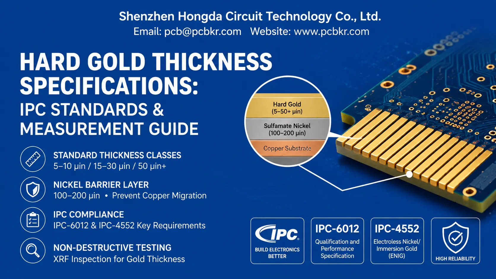
Class 1 (5–10 µin): Light Duty Commercial Class 1 covers single-insertion or low-cycle applications such as consumer expansion cards and test fixtures with fewer than 500 mating cycles. At 5–10 µin (0.127–0.254 µm), the gold layer is thin enough that porosity is a real concern. This class is appropriate only when the connector remains seated for the product lifetime and environmental exposure is minimal.
Class 2 (15–30 µin): Industrial and Dedicated Service Electronics Class 2 represents the commercial sweet spot. A 30 µin (0.762 µm) deposit over 120 µin nickel provides reliable performance for 500–1,000 insertion cycles in industrial controls, networking gear, and medical devices. Most procurement teams specify 30 µin as the default because the cost delta versus 20 µin is marginal, while the wear margin doubles. For digital signals above 1 GHz, skin effect losses and oxidation risks escalate quickly below 30 µin, making this thickness a de facto minimum for high-speed edge connectors.
Class 3 (50 µin+): High-Reliability and Military Edge Connectors Class 3, per IPC-6012F, mandates a minimum 50 µin (1.27 µm) hard gold over a 150 µin (3.81 µm) nickel underplate for mission-critical hardware. Aerospace backplanes, military VPX modules, and automotive ECU interfaces fall into this category. At 50 µin, porosity drops to negligible levels, and the contact interface survives 1,000–5,000 cycles under mechanical stress and thermal shock. For test fixtures and burn-in boards subjected to daily insertion, 75–100 µin is not uncommon.
Procurement Decision Matrix:
| Application | Hard Gold Thickness | Nickel Underplate | Expected Cycles |
|---|---|---|---|
| Consumer / Single Insertion | 5–10 µin | 100 µin | < 500 |
| Industrial / Networking | 30 µin | 120 µin | 500–1,000 |
| Medical / Server | 30–50 µin | 150 µin | 1,000–3,000 |
| Aerospace / Military | 50–100 µin | 150–200 µin | 3,000–10,000 |
Sulfamate Nickel Barrier Layer Thickness and Copper Migration Prevention
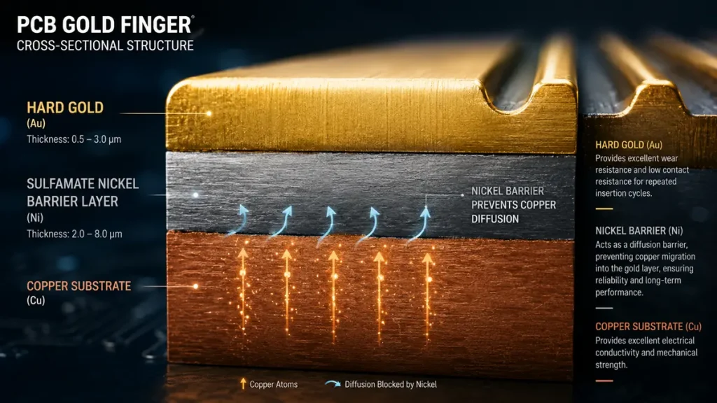
Cross-Sectional Structure of PCB Gold Finger showing Sulfamate Nickel Barrier preventing Copper Migration.
Hard gold cannot deposit directly onto copper. Without an intermediate nickel barrier, copper atoms diffuse into the gold lattice within weeks, forming a porous, high-resistance intermetallic layer that oxidizes and cracks under insertion stress. The nickel underplate is therefore not optional—it is a migration barrier and a mechanical foundation.
Sulfamate nickel chemistry produces a deposit with low internal stress and high ductility, critical for surviving the 30° beveling operation without microcracking. IPC-6012F specifies 100–200 µin (2.54–5.08 µm) for most applications, with 150 µin as the Class 3 baseline. Below 100 µin, copper migration becomes measurable within 6–12 months of thermal cycling. Above 200 µin, the nickel itself can become a stress concentrator at the finger edge, particularly on boards thicker than 3.2 mm.
Procurement teams should verify two nickel parameters beyond thickness: sulfur content must stay below 0.003% to prevent gold embrittlement, and the deposit must be fully bright (not semi-bright) to ensure uniform gold coverage. Request the supplier’s sulfamate bath chemistry log and Hull cell analysis records during the audit.
IPC-6012 vs. IPC-4552 Compliance for Gold Finger PCBs
Two standards govern hard gold edge connectors, and conflating them is a common supplier audit failure. IPC-6012F is the performance specification—it tells you what thickness, adhesion, and thermal stress levels the finished board must survive. IPC-4552 is the process specification for electroplated gold—it defines bath chemistry, cobalt/nickel hardener content (0.2–0.5% for hard gold), hardness (130–200 Knoop), and porosity limits.
A supplier can deliver boards that meet IPC-6012F thickness targets while violating IPC-4552 bath control standards. The result is a gold layer that passes initial electrical test but fails wear testing six months later because cobalt distribution was non-uniform. When qualifying a new vendor, request:
- IPC-6012F Class 3 certificate (or Class 2, as applicable)
- IPC-4552 process audit documentation
- Gold hardness test reports (Knoop or Vickers)
- Porosity test results per IPC-TM-650 2.4.24 (nitric acid vapor)
- Tape adhesion test results per IPC-TM-650 2.4.18
If the supplier cannot produce item 4 and 5, their process control is incomplete regardless of what the XRF thickness report says.
Non-Destructive XRF Gold Thickness Verification Methods
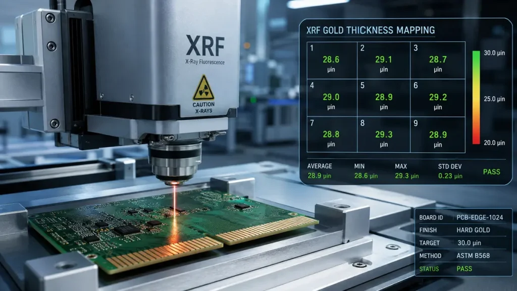
Non-destructive XRF thickness inspection of PCB gold fingers showing a 9-point thickness distribution map per IPC-TM-650 2.4.42.
X-ray fluorescence (XRF) has displaced beta backscatter as the dominant production-line thickness gauge because it measures gold, nickel, and copper simultaneously in under 10 seconds without destroying the coupon. Modern benchtop units with silicon drift detectors (SDD) resolve thickness down to 0.01 µin (0.25 nm), well beyond the tolerance bands of any IPC class.
However, XRF accuracy is not automatic. The instrument must correct for copper substrate thickness variation, especially on multilayer boards where inner copper planes alter the fluorescence ratio. Measurement spot size matters: a 0.1 mm collimator is necessary for fine-pitch gold fingers below 0.5 mm pitch. Count time is equally critical—industry data shows that increasing count time from 5 seconds to 60 seconds improves gage repeatability (Cg) from 0.5 to 1.44, a difference that separates a marginal process from a capable one.
Procurement teams should insist on XRF reports that include:
- Measurement location map (minimum 5 points per finger zone)
- Count time (60 seconds for qualification, 30 seconds for production)
- Calibration traceability to NIST-traceable standards
- Simultaneous Au/Ni/Cu layer decomposition (not just single-layer gold)
Cross-sectional analysis remains the referee method for process validation, but it is destructive and slow. Use it for first-article inspection, not for lot acceptance.
2026 Hard Gold Plating Technology Trends for High-Reliability PCBs
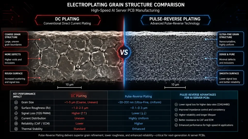
SEM microscopic comparison of grain structures between conventional DC Plating and Pulse-Reverse Electrolytic Gold Plating for high-speed AI server PCBs.
The shift to PCIe Gen 6 (64 GT/s PAM4) and 224G PAM4 AI server backplanes is reshaping gold finger requirements in ways that thickness alone cannot address. At 32 GHz Nyquist frequencies, the edge connector is no longer just a mechanical interface—it is a transmission line stub. Signal integrity teams now model the gold-over-nickel-over-copper stackup as part of the channel simulation, and plating thickness variation directly impacts impedance continuity.
This has driven adoption of pulse-reverse electrolytic gold plating over conventional DC plating. Pulse-reverse systems alternate between forward deposition and reverse etching pulses, producing a finer grain structure with 15–20% higher hardness and significantly better thickness uniformity (±8% across a 24-inch panel versus ±15% for DC). For procurement, this means tighter impedance control and fewer insertion-cycle failures at no significant cost premium.
Material ecosystems have also evolved. AI server boards now pair gold fingers with ultra-low-loss laminates such as Panasonic Megtron 7 (Df 0.0020) or Isola Tachyon 100G. The CTE mismatch between these materials and the gold/nickel stackup creates new thermomechanical stress at the finger edge. Leading fabricators now pre-qualify their plating processes with 1,000-cycle thermal shock tests (–40 °C to +125 °C) specifically for hybrid stackups.
Shenzhen Hongda Circuit’s Advanced Hard Gold Manufacturing Capabilities
At Shenzhen Hongda Circuit Technology Co., Ltd. (PCBkr), our hard gold plating line was purpose-built for edge connector applications rather than adapted from a general-purpose ENIG line. The distinction matters to procurement teams because dedicated equipment eliminates cross-contamination risks and enables process windows that shared lines cannot maintain.
Our pulse-reverse plating system deposits hard gold from 10 µin to 100 µin (0.25 µm to 2.54 µm) over a sulfur-free sulfamate nickel underplate ranging from 100 µin to 300 µin. Three Fischer Technology XRF spectrometers with SDD detectors provide 0.01 µin resolution and automated 9-point mapping on every production panel. CNC beveling centers hold ±1° angle tolerance across 20°–60° profiles, with ionic cleanliness validation after each lot.
For high-speed applications, we integrate plating thickness data into our impedance modeling workflow. Our Keysight N5247B PNA-X TDR analyzer verifies that the additional gold and nickel buildup at the finger pad does not push differential impedance outside the ±5% tolerance band. This is particularly critical for PCIe Gen 6 and CXL 3.0 cards where a 2-ohm mismatch at the connector can close the PAM4 eye.
Quality certifications include IPC-6012F Class 3/3A, AS9100D, IATF 16949, and ISO 13485. Every lot ships with a full documentation package: XRF thickness certificates, cross-sectional micrographs, thermal cycle data, and material traceability reports. For procurement teams auditing Chinese suppliers, we provide virtual factory tours and real-time MES traceability dashboards upon request.
Gold Finger PCB Procurement Checklist for Buyers
Use this checklist during RFQ qualification and incoming inspection:
- Specify the standard explicitly: State IPC-6012F Class 2 or Class 3, not just a thickness number.
- Define nickel underplate minimum: 120 µin for Class 2, 150 µin for Class 3. Do not let the supplier default to “standard” nickel.
- Request XRF distribution data: Minimum, maximum, and average across the panel, not a single-point reading.
- Validate bevel angle and tolerance: 30° ±1° is standard; confirm your connector datasheet compatibility.
- Demand adhesion and porosity data: IPC-TM-650 2.4.18 tape test and 2.4.24 nitric acid vapor test results.
- Verify plating line dedication: Confirm hard gold is plated in-house on a dedicated line, not outsourced or shared with ENIG.
- Check impedance compensation: For high-speed cards, ask how the fabricator accounts for plating buildup in the finger pad area.
- Audit certification scope: Ensure the supplier’s IPC-6012 and AS9100 certificates are current and cover your specific product category.
Frequently Asked Questions (FAQ)
What is the minimum hard gold thickness required for IPC-6012 Class 3 gold finger PCBs?
IPC-6012F mandates a minimum of 30 µin (0.762 µm) hard gold for Class 3, but in practice, most high-reliability edge connectors specify 50 µin (1.27 µm) to achieve 1,000+ insertion cycles. The nickel underplate must be at least 150 µin (3.81 µm). Always pair the gold thickness with the correct nickel barrier—thin gold over inadequate nickel is a common failure mode.
How does sulfamate nickel underplate thickness prevent copper migration in edge connectors?
Sulfamate nickel acts as a diffusion barrier. Copper atoms migrate through grain boundaries at room temperature; a 150 µin nickel layer with low sulfur content (<0.003%) slows this migration by orders of magnitude. Without it, copper forms an oxide-rich intermetallic with the gold within months, raising contact resistance and creating crack initiation points under mechanical wear.
What is the difference between XRF and cross-sectional analysis for gold thickness measurement?
XRF is non-destructive and measures gold, nickel, and copper simultaneously in seconds, making it ideal for production lot acceptance. Cross-sectional analysis is destructive but provides a direct physical view of layer structure and is used for first-article validation and process qualification. Procurement teams should require XRF reports for every lot and cross-sections for initial supplier qualification.
Why should procurement teams specify pulse-reverse electrolytic gold plating over conventional DC plating?
Pulse-reverse plating produces a finer grain structure with higher hardness and ±8% thickness uniformity across large panels, compared to ±15% for DC plating. For high-speed applications like PCIe Gen 6, this uniformity translates to consistent impedance at the finger pad and longer insertion cycle life. The cost delta is typically less than 5%, making it a high-ROI specification for critical boards.
What certifications should I verify when auditing a hard gold PCB manufacturer in China?
Minimum baseline: ISO 9001:2015 and IPC-A-600. For mission-critical hardware, require IPC-6012F Class 3/3A, IPC-4552 process compliance, and industry-specific certifications: AS9100D for aerospace, IATF 16949 for automotive, and ISO 13485 for medical. Request the actual certificate scope pages—not just logos on a brochure—to confirm the certification body has audited the specific plating processes you are buying.
Company: Shenzhen Hongda Circuit Technology Co., Ltd.
Website:www.pcbkr.com
Email:sales@pcbkr.com
Certifications: IPC-6012F Class 3/3A | AS9100D | IATF 16949 | ISO 13485
Ready to specify your next hard gold PCB? Upload your Gerber files and stackup requirements to sales@pcbkr.com for a complimentary DFM review and plating specification recommendation within 30 minutes.
About Author
David Chen https://www.linkedin.com/in/pcbcoming
David Chen boasts an extensive professional background in PCBA manufacturing, PCBA testing, and PCBA optimization, with specialized expertise in high-precision PCBA fault analysis and rigorous PCBA reliability testing. The author has worked with high-layer-count server PCB fabrication, ultra-low-loss backplane stackups, and thermo-mechanical reliability optimization for AI infrastructure projects involving 112G and 224G PAM4 architectures. Skilled in complex circuit design and cutting-edge advanced PCB manufacturing processes, he delivers solutions that elevate product durability and performance across industrial applications. His technical articles focusing on PCBA manufacturing workflows and testing methodologies are widely cited by industry peers, research institutions, and technical platforms, solidifying his reputation as a recognized technical authority in the global circuit board manufacturing sector.