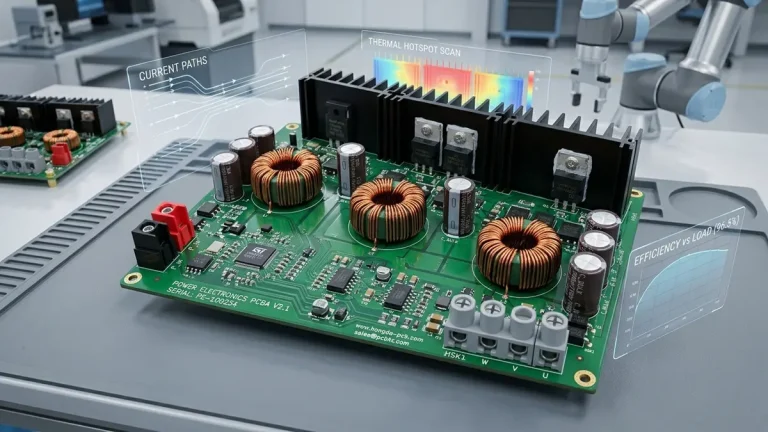
Controlled Impedance PCB Manufacturer: Fabrication, TDR Testing & Quality Control
Selecting a controlled impedance PCB manufacturer requires more than finding a factory that can produce 50Ω or 100Ω traces. OEM buyers must verify whether the manufacturer can translate electrical requirements into a manufacturable stackup, control critical fabrication variables, and provide appropriate measurement evidence for the finished boards.
Shenzhen Hongda Circuit Technology Co., Ltd. manufactures precision multilayer PCBs using LDI imaging, controlled lamination, laser drilling, mSAP processing, automated inspection, and electrical testing. Our engineering team supports project-based reviews of impedance requirements, PCB stackup construction, material selection, and manufacturing feasibility.
This guide explains how to evaluate controlled impedance PCB fabrication, what manufacturing capabilities matter, how TDR verification should be specified, and what procurement teams should include in an RFQ before releasing production.
What Should You Expect from a Controlled Impedance PCB Manufacturer?
A controlled impedance PCB manufacturer should be able to connect five elements:
- Electrical requirements and target impedance.
- PCB material and stackup construction.
- Trace geometry and manufacturing tolerances.
- Fabrication process control.
- Electrical verification and documented acceptance.
A controlled impedance PCB is designed and manufactured so that specified transmission-line structures achieve their target characteristic impedance within an agreed tolerance.
Common examples include:
- 50Ω single-ended transmission lines.
- 75Ω single-ended structures where required by the application.
- 85Ω differential pairs.
- 90Ω differential pairs.
- 100Ω differential pairs.
These values are application-dependent design requirements, not universal manufacturing specifications.
For example, a high-speed digital interface may require a defined differential impedance, while an RF connection may use a single-ended transmission line.
The manufacturer must understand which structures require impedance control, which layers contain those structures, and which reference planes define their electrical behavior.
What buyers should verify
Before selecting a supplier, request confirmation of:
- Whether the factory can manufacture the required layer count and stackup.
- Whether the specified laminate and copper construction are available.
- Whether the controlled trace geometry is compatible with its imaging and etching processes.
- Whether proposed stackup or geometry changes require customer approval.
- Whether impedance verification is included in the quotation.
- Whether measurement reports can be supplied with the production lot.
A supplier that only confirms a nominal impedance value without reviewing the actual construction has not completed a meaningful manufacturing feasibility assessment.
What PCB Specifications Are Required for Controlled Impedance Manufacturing?
An impedance requirement must be defined clearly enough for engineering, CAM, production, and quality inspection to work from the same information.
A fabrication drawing that simply states “50Ω controlled impedance” is incomplete.
The manufacturer needs to know where the controlled impedance structures are located and how their electrical requirements relate to the physical PCB construction.
1. Target impedance and tolerance
Specify the nominal impedance and permitted deviation for each controlled structure.
For example:
| Structure | Example target | Example tolerance |
|---|---|---|
| Single-ended signal | 50Ω | ±10% |
| Differential pair | 90Ω | ±10% |
| Differential pair | 100Ω | ±10% |
These are illustrative RFQ examples, not guaranteed PCBKR production tolerances. The actual acceptance window must be agreed after reviewing the design and manufacturing construction.
A tighter tolerance may require additional engineering review, more restrictive material and geometry controls, and a defined measurement plan.
Do not automatically specify the tightest possible tolerance on every signal. Apply requirements according to the interface specification and system signal-integrity budget.
2. Signal layers and reference planes
Identify every layer that contains controlled impedance traces.
For each structure, provide:
- Signal layer number.
- Reference plane layer.
- Single-ended or differential configuration.
- Target impedance.
- Nominal trace width.
- Differential spacing, where applicable.
- Controlled net names or net classes.
The reference plane is particularly important because the distance between the signal conductor and its reference structure directly affects characteristic impedance.
A 50Ω trace on an outer-layer microstrip structure is not geometrically equivalent to a 50Ω trace embedded in an inner-layer stripline structure.
3. Trace width and differential spacing
Trace width and spacing influence the electric and magnetic field distribution around the transmission line.
For differential pairs, the coupling between the two conductors also affects differential impedance.
Buyers should identify whether the supplied artwork geometry is fixed or whether the manufacturer may propose width and spacing adjustments.
This distinction prevents a common manufacturing problem: the factory modifies the trace geometry to achieve its calculated target, but the customer has not authorized the change.
4. Finished copper and dielectric construction
The impedance calculation must reflect the intended finished PCB construction.
Relevant parameters include:
- Base copper thickness.
- Finished copper thickness.
- Dielectric thickness.
- Laminate and prepreg construction.
- Material dielectric constant (Dk).
- Dissipation factor (Df).
- Reference plane configuration.
- Surface solder mask conditions.
The manufacturer should review these parameters together rather than calculate impedance from trace width alone.
How Does PCBKR Control Impedance During PCB Fabrication?
Controlled impedance is influenced by several connected manufacturing operations. A stable result depends on the relationship between the approved stackup, copper geometry, dielectric construction, and process execution.
At Shenzhen Hongda Circuit Technology, the manufacturing review can be organized into the following stages.
Stage 1: Engineering and stackup review
Before production, the engineering team reviews the customer’s electrical and physical requirements.
The review considers:
- Layer count and layer assignment.
- Target impedance and tolerance.
- Signal-to-reference-plane relationships.
- Material requirements.
- Copper thickness.
- Dielectric construction.
- Finished board thickness.
- Manufacturing feasibility.
If the customer’s proposed stackup is not compatible with the requested electrical target or manufacturing construction, the proposed changes should be reviewed and approved before production release.
This prevents the factory from making unapproved changes to the customer’s design.
Stage 2: Material selection and lamination
Dielectric properties influence characteristic impedance.
Material selection must consider more than a nominal Dk value. The actual construction, resin content, cured dielectric thickness, copper foil, and operating frequency can all influence electrical performance.
For multilayer boards, the lamination process determines the final relationship between signal layers and reference planes.
PCBKR uses LAUFFER lamination equipment with controlled pressure and vacuum processing.
Documented equipment parameters include:
- Lamination pressure settings of 80, 150, and 200 psi.
- Vacuum level below 50 mbar.
These are equipment process parameters, not universal recipes for every PCB stackup. The appropriate lamination program depends on the selected materials, layer construction, and project requirements.
Stage 3: Imaging and copper pattern formation
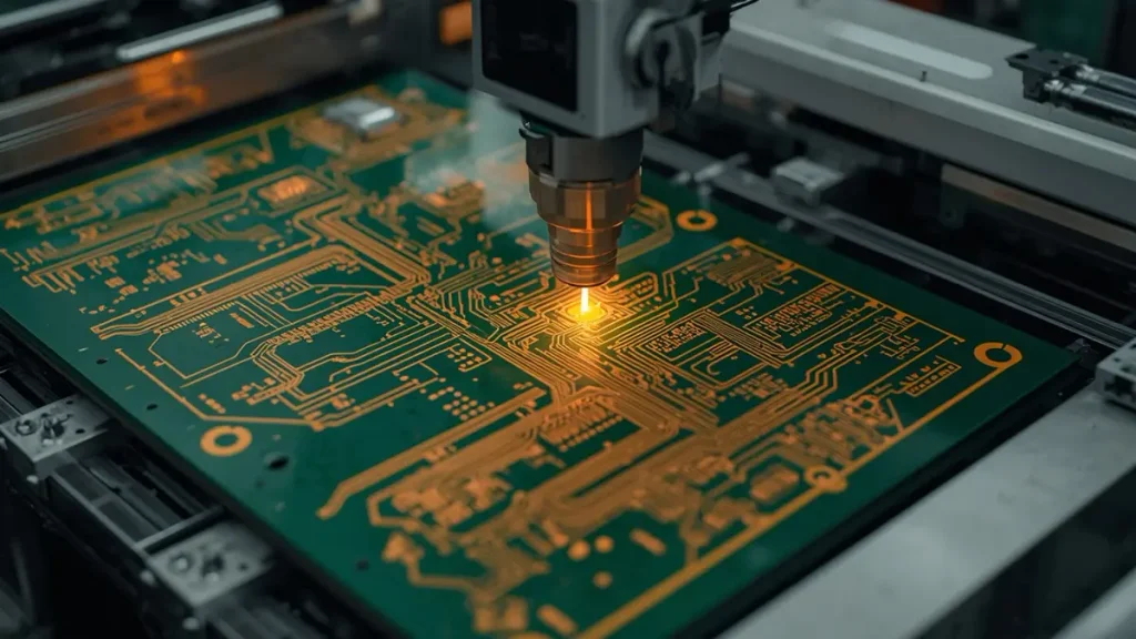
Precision LDI Imaging and Copper Pattern Formation for Controlled Impedance PCB Manufacturing
The finished trace geometry affects impedance.
PCBKR uses SCREEN Ledia LDI equipment for precision circuit imaging.
The documented fine-line imaging target is 8µm, with a ±10µm process registration target.
The imaging process is important because inaccurate circuit pattern transfer can affect:
- Trace width.
- Differential pair spacing.
- Signal-to-plane alignment.
- Fine-line geometry.
- Layer-to-layer registration.
The final conductor dimensions also depend on copper thickness and the subsequent etching and plating processes.
For advanced fine-line structures, PCBKR has implemented mSAP processing with documented 8/8µm line/space capability since Q3 2024.
This is an advanced circuit fabrication capability. It should not be interpreted as a universal minimum geometry for every controlled impedance design.
Stage 4: Laser drilling and multilayer interconnection
Via structures can introduce impedance discontinuities, particularly in high-speed signal paths.
PCBKR uses Mitsubishi UV/CO₂ laser processing for microvia fabrication.
Documented process capability includes:
- UV/CO₂ laser microvia processing down to 75µm with ±5µm capability.
- Picosecond laser processing down to 50µm.
These technologies support advanced multilayer and HDI constructions.
For high-speed designs, buyers should also identify whether via stubs, backdrilling, via-in-pad, or other special structures are part of the electrical design.
The PCB manufacturer should review these features during DFM rather than treating impedance as an isolated trace-width requirement.
Stage 5: Inspection and electrical verification
Manufacturing inspection helps identify physical defects that may affect the finished board.
PCBKR’s documented inspection and testing equipment includes:
- 3D AOI.
- X-ray inspection.
- Four-wire Kelvin flying probe testing.
- TDR testing for project-specific impedance verification.
- VNA capability up to 70GHz.
These methods have different purposes.
AOI checks visible circuit features. X-ray inspection supports examination of internal structures. Four-wire Kelvin measurement is used for low-resistance electrical measurements. TDR and VNA are used for different aspects of high-frequency electrical characterization.
The applicable verification method, sampling scope, and reporting requirements must be defined for each project.
How Do Materials and Stackup Affect Finished PCB Impedance?
Material selection and stackup construction are fundamental to controlled impedance PCB manufacturing.
A trace cannot be assigned a reliable impedance value without considering the surrounding dielectric and conductor geometry.
Dielectric constant (Dk)
Dk affects the effective dielectric environment surrounding a transmission line.
Different laminate materials and constructions can produce different impedance values even when trace width and spacing remain unchanged.
When selecting materials, engineering should consider:
- Material manufacturer and grade.
- Published Dk data and its test conditions.
- Operating frequency.
- Resin content and glass style.
- Dielectric thickness after lamination.
- Compatibility with the complete stackup.
Do not treat a catalog Dk value as an unconditional production guarantee.
Dissipation factor (Df)
Df describes dielectric energy loss.
For high-speed and high-frequency applications, material loss becomes increasingly important alongside impedance control.
A design can achieve its nominal impedance while still experiencing unacceptable signal attenuation.
For this reason, buyers should evaluate insertion loss and other channel requirements separately from characteristic impedance.
Copper thickness and surface geometry
Copper thickness affects the effective transmission-line geometry.
The finished trace profile may also differ from the ideal rectangular cross-section assumed by a simplified calculation.
Manufacturing review should consider:
- Starting copper thickness.
- Finished copper thickness.
- Pattern plating.
- Etching effects.
- Trace width and spacing.
- Surface copper conditions.
These variables should be incorporated into the manufacturer’s feasibility review.
Microstrip and stripline stackups
Microstrip
Microstrip structures are typically routed on an outer signal layer with a reference plane beneath the dielectric.
Their impedance is influenced by trace width, dielectric thickness, material properties, copper thickness, and solder mask.
Stripline
Stripline structures are embedded between reference planes.
Their impedance depends on the conductor geometry and the dielectric environment surrounding the signal.
Neither structure is automatically better for every application. The correct choice depends on routing architecture, signal integrity, material selection, and manufacturing feasibility.
For additional engineering information, see PCBKR’s High-Speed PCB manufacturing capabilities and High-Frequency PCB manufacturing information.
How Are PCB Trace Geometry and Registration Controlled?
A controlled impedance design can fail even when the laminate material is correct.
The reason is that the final copper geometry may differ from the original CAD artwork.
Trace width and etching
Chemical etching changes the conductor profile.
The final trace may have a trapezoidal cross-section rather than an ideal rectangle.
This means the manufacturer must consider the actual production geometry when reviewing impedance requirements.
Etching-related variables include:
- Copper thickness.
- Circuit density.
- Layer position.
- Etching compensation.
- Final trace width.
- Trace spacing.
The appropriate compensation depends on the specific manufacturing construction.
Differential pair spacing
Differential impedance depends on both the individual conductor geometry and the coupling between the two traces.
Changes in pair spacing can alter the coupling and therefore the differential impedance.
For this reason, differential pair spacing should be explicitly identified in the impedance table.
Registration and reference-plane alignment
Layer-to-layer registration is important when controlled impedance structures depend on a specific relationship between signal traces and reference planes.
PCBKR’s documented LDI process supports precision circuit imaging with an 8µm target and ±10µm registration target.
However, the actual electrical impact of registration depends on the stackup and signal structure.
Manufacturing feasibility should be assessed against the customer’s specific design rather than assuming that one imaging specification automatically guarantees an impedance tolerance.
How Is Controlled Impedance Verified by TDR Testing?

TDR Impedance Testing of PCB Transmission Line Coupons for Electrical Verification
Time-domain reflectometry (TDR) is commonly used to evaluate characteristic impedance along a transmission-line test structure.
A TDR instrument launches a fast electrical signal into the structure and evaluates reflected signals caused by impedance changes.
For PCB manufacturing, test coupons are frequently used because they provide accessible structures for measurement.
What is a PCB impedance test coupon?
An impedance coupon is a representative test structure manufactured as part of a production panel or another agreed test arrangement.
It can reproduce selected features of the production PCB, including:
- Signal trace geometry.
- Dielectric construction.
- Copper thickness.
- Reference-plane configuration.
- Single-ended or differential structure.
The coupon should be designed or approved with the actual production stackup in mind.
A coupon that does not represent the relevant board construction may produce results that are difficult to correlate with the product.
What should a TDR report include?
For procurement and quality acceptance, buyers should agree on the report contents before production.
A useful report should identify:
| Report item | Information required |
|---|---|
| Order identification | Customer PO or manufacturing order |
| PCB revision | Released fabrication revision |
| Test structure | Coupon identification |
| Impedance target | Nominal impedance |
| Tolerance | Approved acceptance range |
| Measured result | Actual measured impedance |
| Test method | Agreed measurement procedure |
| Pass/fail result | Acceptance decision |
| Test date | Measurement date |
| Traceability | Link to the applicable production lot |
Where required, buyers can also request the TDR waveform, coupon photographs, and related engineering records.
The actual deliverables should be agreed in the quotation or purchase specification.
Can a TDR coupon prove that the complete PCB will work?
No.
A passing coupon result provides evidence about the tested representative transmission-line structure.
It does not independently prove the performance of every signal path on the assembled product.
The complete electrical channel may also include:
- Connector launches.
- BGA escape routing.
- Via transitions.
- Backdrilled structures.
- Plane changes.
- Package interconnects.
- Cable interfaces.
These features can introduce additional discontinuities and losses.
TDR and VNA measurements also answer different questions. TDR helps examine impedance variations in the time domain, while VNA measurements can characterize frequency-dependent behavior such as S-parameters.
For high-speed or RF products, the system-level validation plan should be defined separately from PCB fabrication acceptance.
What Should Buyers Verify Before Selecting a PCB Manufacturer?
A manufacturer’s website is only the starting point for supplier qualification.
OEM procurement teams should verify whether the factory can support the actual board construction and provide the required manufacturing evidence.
Use the following supplier audit checklist.
1. Manufacturing equipment
Ask whether the supplier has the necessary equipment for:
- Precision circuit imaging.
- Multilayer lamination.
- Mechanical and laser drilling.
- Fine-line processing.
- Automated optical inspection.
- X-ray inspection.
- Electrical testing.
- High-frequency verification where required.
Ask for the equipment model, applicable process limits, and supporting evidence rather than accepting a general capability statement.
2. Stackup and material control
Verify:
- Whether the supplier can review customer-proposed stackups.
- Whether material grades can be specified and controlled.
- Whether substitutions require approval.
- Whether finished dielectric thickness is considered.
- Whether copper thickness is reviewed against the impedance design.
- Whether the final stackup is approved before production.
3. Process capability and repeatability
Ask the manufacturer to distinguish among:
- Equipment specifications.
- Engineering design targets.
- Demonstrated process capability.
- Project-specific qualified results.
- Mass-production acceptance criteria.
A Cpk value is meaningful only when it is supported by a defined characteristic, specification limits, representative measurements, and an appropriate statistical dataset.
Do not accept a general Cpk claim as proof of impedance consistency without reviewing the underlying data.
4. Inspection and test documentation
Confirm which inspection methods apply to the project.
Depending on the PCB construction and customer requirements, the documentation package may include:
- Electrical test reports.
- TDR impedance reports.
- VNA measurement records.
- AOI inspection records.
- X-ray inspection records.
- Cross-section reports.
- Material certificates.
- Certificate of Conformance.
Not every order requires every report. Define the required inspection scope before placing the purchase order.
5. Production revision and traceability
A common source of manufacturing disputes is a mismatch between the approved engineering revision and the files used in production.
Ask the supplier to confirm:
- Which fabrication revision was released.
- Whether the approved stackup matches the production construction.
- Whether material substitutions were authorized.
- How production lots are identified.
- How nonconforming results are reported.
- How rework or replacement decisions are approved.
This is particularly important when prototype and mass-production orders are released at different times.
How Does Controlled Impedance Affect PCB Manufacturing Cost?
Controlled impedance PCB pricing depends on more than the nominal impedance value.
The total manufacturing cost is influenced by the physical construction, material selection, process complexity, testing requirements, and production quantity.
1. Material selection
Specialized low-loss laminates can cost more than standard FR-4 materials.
Material availability, minimum purchasing quantities, and approved material substitutions may also affect lead time and cost.
2. Layer count and stackup complexity
Higher layer counts and complex stackups generally require more engineering and manufacturing coordination.
Sequential lamination, HDI microvias, and special dielectric constructions may add process steps.
3. Trace geometry and copper requirements
Very fine trace widths, narrow differential spacing, and unusual copper constructions may require additional manufacturing controls.
The feasibility of a particular impedance requirement depends on the complete geometry, not just the target value.
4. Impedance tolerance
Tighter impedance tolerance may require additional engineering review, more restrictive process conditions, and a more detailed measurement plan.
Buyers should avoid specifying unnecessarily tight tolerances on noncritical signals.
5. Testing and documentation
The quotation should distinguish between:
- Standard electrical testing.
- Impedance coupon fabrication.
- TDR testing.
- VNA characterization.
- Additional inspection.
- Physical coupon delivery.
- Detailed test reporting.
This prevents suppliers from quoting different test scopes while appearing to offer the same price.
6. Production quantity and yield risk
Prototype, pilot, and mass-production orders have different setup and material economics.
A lower unit price is not necessarily the lowest total procurement cost if it excludes engineering, testing, or quality documentation required for product release.
When comparing quotations, evaluate the complete scope of supply rather than the unit price alone.
What Should an OEM Include in a Controlled Impedance PCB RFQ?
An effective RFQ should allow the PCB manufacturer to evaluate the electrical requirements, determine the manufacturing construction, and quote the same acceptance scope.
The following checklist can be used when requesting a controlled impedance PCB quotation.
A. PCB fabrication information
- Gerber or ODB++ fabrication files.
- NC drill files.
- Fabrication drawing.
- Board outline and dimensions.
- Layer count.
- Finished board thickness.
- Copper thickness requirements.
- Surface finish.
- Quantity and production forecast.
B. Impedance requirements
- Target impedance for each controlled structure.
- Permitted impedance tolerance.
- Single-ended or differential configuration.
- Signal layer assignment.
- Reference-plane assignment.
- Controlled net names or net classes.
- Nominal trace width.
- Differential pair spacing.
- Solder mask conditions.
- Applicable frequency or interface requirements.
C. Material and stackup requirements
- Required laminate manufacturer.
- Material grade.
- Dk/Df requirements and relevant frequency conditions.
- Core and prepreg construction.
- Finished dielectric thickness.
- Copper foil requirements.
- Approved material alternatives.
- Customer-approved stackup constraints.
D. Manufacturing change approval
The buyer should clearly state:
- Whether the supplier may propose trace-width adjustments.
- Whether pair spacing can be changed.
- Whether the supplier may propose alternative materials.
- Whether stackup changes require written approval.
- Which revision is authorized for production.
This section is important because a manufacturer may need to adjust physical geometry to accommodate actual manufacturing conditions.
However, any change affecting the customer’s electrical design constraints must follow an agreed approval process.
E. Testing and acceptance
Specify:
- Whether impedance coupons are required.
- Which structures must be measured.
- Whether TDR testing is required.
- Whether VNA measurements are separately required.
- Required measurement sampling.
- Acceptance tolerance.
- Test report format.
- Whether physical coupons must be returned.
- Procedure for out-of-specification results.
F. Commercial requirements
- Prototype quantity.
- Pilot production quantity.
- Mass-production forecast.
- Required delivery date.
- Packaging requirements.
- Inspection documentation.
- Applicable quality standards.
- Shipping destination.
A complete RFQ reduces quotation uncertainty, prevents unapproved engineering changes, and makes supplier comparison more meaningful.
Why Choose Shenzhen Hongda Circuit Technology for Controlled Impedance PCB Manufacturing?
Shenzhen Hongda Circuit Technology Co., Ltd. is a PCB manufacturing factory in Shenzhen, China, supporting precision multilayer PCB fabrication and advanced interconnection technologies.
For controlled impedance projects, manufacturing feasibility depends on the complete relationship between material construction, trace geometry, layer registration, lamination, and electrical verification.
PCBKR’s documented manufacturing resources include:
Precision imaging
SCREEN Ledia LDI equipment with an 8µm imaging target and ±10µm registration target.
Multilayer lamination
LAUFFER lamination equipment with documented pressure settings of 80, 150, and 200 psi, and vacuum processing below 50 mbar.
Laser drilling
Mitsubishi UV/CO₂ laser processing with documented 75µm microvia capability and ±5µm process capability, together with picosecond laser processing down to 50µm.
Advanced fine-line fabrication
mSAP processing with documented 8/8µm line/space capability since Q3 2024.
Inspection and testing
3D AOI, X-ray inspection, four-wire Kelvin flying probe testing, and project-specific TDR/VNA verification capabilities, including VNA measurement capability up to 70GHz.
These resources support complex multilayer, HDI, and precision PCB manufacturing.
The exact achievable impedance tolerance, material construction, inspection scope, and production acceptance criteria must still be confirmed against each customer’s design.
For related manufacturing capabilities, see our HDI PCB manufacturing information.
If your project requires impedance modeling, stackup review, or additional engineering discussion, our team can review the requirements before production.
Submit your Gerber or ODB++ files, stackup requirements, impedance table, and target quantity to request a project-specific manufacturing review.
Shenzhen Hongda Circuit Technology Co., Ltd.
Website: https://www.pcbkr.com/
Email: sales@pcbkr.com
Frequently Asked Questions About Controlled Impedance PCB Manufacturing
What is a controlled impedance PCB?
A controlled impedance PCB is a circuit board in which specified transmission-line structures are designed and manufactured to achieve a defined characteristic impedance within an agreed tolerance. Its performance depends on trace geometry, dielectric properties, copper thickness, and reference-plane configuration.
What is the standard impedance tolerance for PCB manufacturing?
There is no single tolerance that applies to every controlled impedance PCB project. ±10% is a commonly encountered design and manufacturing specification, while tighter tolerances may be required for particular high-speed applications. The achievable tolerance must be reviewed and agreed for the actual material, stackup, geometry, and test method.
What is the difference between 50Ω single-ended and 100Ω differential impedance?
50Ω single-ended impedance describes one signal conductor relative to its reference structure. 100Ω differential impedance describes the electrical behavior of a coupled pair of conductors. Differential impedance depends on both trace geometry and the spacing between the two traces, so a 100Ω differential pair is not simply two independent 50Ω traces.
Can a PCB manufacturer change trace width to achieve the target impedance?
A manufacturer may propose adjustments to trace width or differential spacing after reviewing the actual material and stackup. However, these changes should be documented and approved according to the customer’s design constraints. Unapproved geometry changes can affect routing clearances, differential coupling, and signal integrity.
Is TDR testing required for every controlled impedance PCB?
TDR testing is commonly used to verify controlled impedance structures, often through representative production coupons. Whether testing is required for every order, every panel, or selected samples depends on the project specification and purchase agreement. Buyers should define the test scope and reporting requirements before production.
Does a passing TDR coupon guarantee that the complete PCB will pass signal integrity testing?
No. A TDR coupon verifies a representative transmission-line structure, not every feature of the complete signal channel. Connectors, vias, BGA transitions, plane changes, and other discontinuities may affect system-level performance. Additional TDR, VNA, S-parameter, or system-level testing may be required depending on the application.
What files are required to obtain a controlled impedance PCB quotation?
A typical RFQ package includes Gerber or ODB++ files, NC drill data, a fabrication drawing, layer stackup, material requirements, impedance targets, tolerances, controlled signal layers, reference planes, trace widths, differential spacing, quantity, and required testing documentation. A complete package helps the manufacturer review feasibility and prepare a comparable quotation.
What is the difference between TDR and VNA testing for controlled impedance PCBs?
TDR evaluates impedance changes along a transmission line in the time domain and is commonly used for impedance coupon verification. A vector network analyzer measures frequency-dependent network behavior, including S-parameters such as insertion loss and return loss. They provide different types of electrical evidence and should be selected according to the product’s validation requirements.
About Author
David Chen LinkedIn Profile
David Chen is a Senior RF/PCB Process Engineer at Shenzhen Hongda Circuit Technology Co., Ltd., with over 12 years of experience in high-frequency PCB fabrication, impedance-controlled stack-up design, and Rogers/PTFE laminate processing. He also boasts an extensive professional background in PCBA manufacturing, PCBA testing, and PCBA optimization, with specialized expertise in high-precision PCBA fault analysis and rigorous PCBA reliability testing. The author has worked with high-layer-count server PCB fabrication, ultra-low-loss backplane stackups, and thermo-mechanical reliability optimization for AI infrastructure projects involving 112G and 224G PAM4 architectures. Skilled in complex circuit design and cutting-edge advanced PCB manufacturing processes, he delivers solutions that elevate product durability and performance across industrial applications. His technical articles focusing on PCBA manufacturing workflows and testing methodologies are widely cited by industry peers and technical platforms, and have gained attention and recognition from industry colleagues.