RF Microwave Teflon PCB: A Strategic Sourcing Guide for High-Frequency Systems
RF Microwave PCB: The global RF and microwave PCB material market was valued at USD 2.31 billion in 2025 and is projected to reach USD 3.78 billion by 2032, driven by the relentless expansion of 5G‑Advanced infrastructure, automotive radar ecosystems, and low‑earth‑orbit satellite constellations.
For procurement professionals and hardware engineering managers, this growth creates both opportunity and risk: the surge in demand for PTFE RF PCB substrates has outpaced the supply of qualified RF PCB manufacturers capable of processing fluoropolymer materials at millimeter‑wave precision.
This guide is written for the technical buyer. It moves beyond generic capability lists and examines the Microwave PCB supplier evaluation criteria that determine first‑pass success—from plasma activation protocols for Teflon laminates to 224Gbps PAM4 signal integrity validation. Whether you are sourcing for Ka‑band satellite terminals, 77 GHz automotive radar, or 5G mmWave base stations, the following framework aligns procurement decisions with 2026 manufacturing realities.
What Makes PTFE RF PCB the Foundation of mmWave Procurement
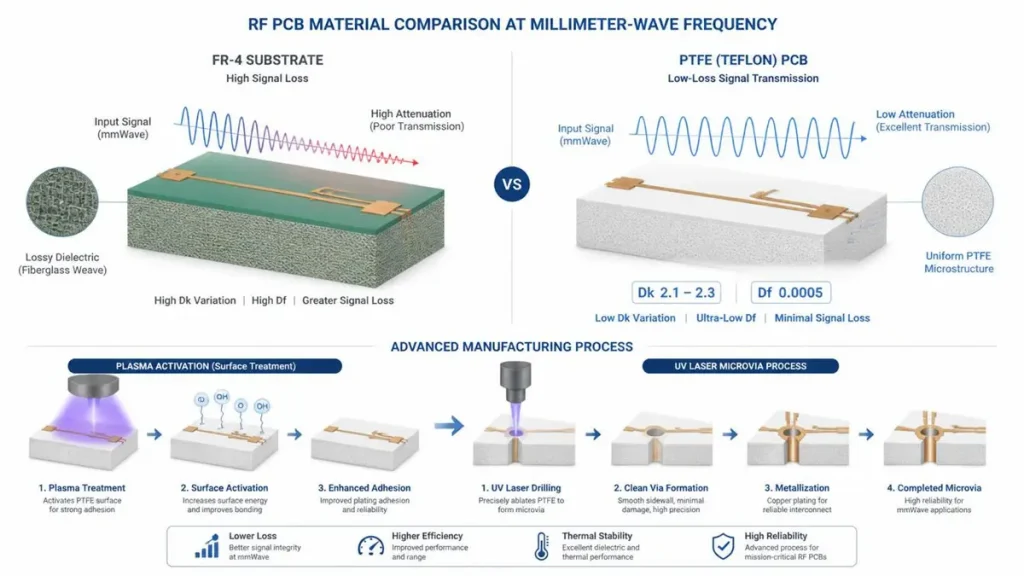
RF PCB Material Comparison at Millimeter-Wave Frequency: FR-4 vs PTFE Substrate with Plasma & UV Laser Process
The Material Science Behind Teflon PCB Performance
At frequencies above 10 GHz, standard FR-4 substrates become electrically lossy and dimensionally unstable. This is why PTFE RF PCB technology—specifically polytetrafluoroethylene-based laminates—dominates procurement specifications for microwave and millimeter-wave applications. PTFE delivers a dielectric constant (Dk) between 2.1 and 2.3 and a dissipation factor (Df) as low as 0.0005 at 10 GHz, parameters that directly govern insertion loss and phase stability.
For procurement teams, this translates into a non-negotiable requirement: your RF PCB manufacturer must demonstrate direct experience with fluoropolymer processing. PTFE is chemically inert and mechanically soft. Without plasma activation or controlled oxidation prior to copper cladding, adhesion fails. Without low-chip-load drilling or UV laser microvia formation, hole-wall quality degrades and impedance uniformity collapses.
These are not standard PCB processes; they are specialized competencies that separate commodity fabricators from high-frequency partners.
Hybrid Stackup Economics: Controlling Teflon PCB Cost
Pure PTFE multilayer constructions can escalate material costs by 40–60% compared to FR-4. Leading procurement strategies now specify hybrid RF stackups—placing PTFE RF layers only where signal integrity demands it, while using high-speed FR-4 or ceramic-filled laminates for digital and power planes. This approach can reduce substrate costs by 30–50% without compromising mmWave performance.
When issuing an RFQ, buyers should demand that the Microwave PCB supplier document bonding compatibility between dissimilar dielectrics, CTE-matched lamination cycles, and controlled-impedance transitions at material boundaries. A supplier that cannot provide solver-correlated TDR coupons for hybrid constructions is a liability at 28 GHz and above.
Evaluating a Microwave PCB Supplier: Technical Benchmarks Buyers Must Verify
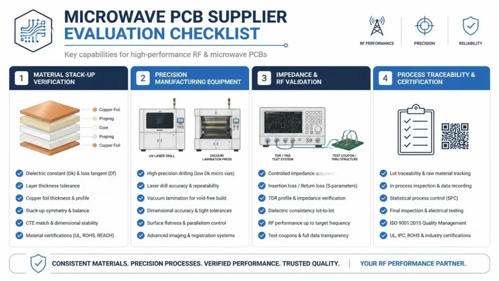
High-Performance Microwave & RF PCB Supplier Evaluation Checklist
From RFQ to First Article: The Procurement Decision Chain
The difference between a successful high-frequency program and a six-month respin often lies in what happens before the purchase order. Professional buyers now structure RFQ packages around the following technical validation gates:
1. Material and Stackup Verification A qualified RF PCB manufacturer should review your impedance table, frequency range, and loss budget before quoting.
Request documentation of the supplier’s approved vendor list for low-Dk materials: Rogers RO4350B, RT5880, Taconic TLY, Megtron 6/7/8, and M9-grade hydrocarbon laminates. If your design operates above 40 GHz, verify that the supplier stocks rolled or very-low-profile (VLP) copper foils to mitigate skin-effect conductor loss.
2. Precision Manufacturing Equipment Audit In 2026, Microwave PCB supplier capability is defined by equipment, not promises. For PTFE processing, the factory must have:
- Multi-wavelength laser drilling systems (UV/CO₂ hybrid) for 0.1 mm microvias with ±25 μm positional accuracy;
- Plasma etching or chemical activation lines specifically for fluoropolymer surface preparation;
- Vacuum lamination presses with staged temperature/pressure profiles to prevent PTFE voiding and warpage;
- LDI (Laser Direct Imaging) exposure for fine-line geometries down to 20 μm line/space.
3. Impedance Control and RF Validation Infrastructure Standard electrical test (E-test) proves continuity, not RF performance. Buyers must confirm that the supplier operates Time-Domain Reflectometry (TDR) for impedance verification and Vector Network Analysis (VNA) for S-parameter measurement up to the target operating frequency.
For 5G mmWave and radar applications, request coupon-based correlation between electromagnetic field solver predictions and fabricated board measurements.
4. Process Traceability and Quality Certifications For aerospace, defense, and automotive radar programs, traceability is non-negotiable. Verify ISO 9001, IPC Class 3, and—where applicable—AS9100 or IATF 16949 certifications.
The supplier should provide lot-linked material certificates, process control data, and a documented change-management protocol.
2026 Manufacturing Technology Trends Reshaping RF PCB Procurement
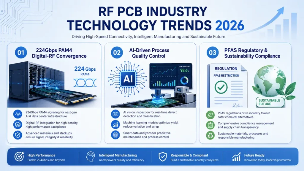
Three Major Technology Trends in the RF PCB Industry for 2026: 224G PAM4, AI-Driven Quality Control, and PFAS Environmental Compliance
224Gbps PAM4 and the Convergence of Digital and RF Domains
The boundary between “digital” and “RF” PCB fabrication has dissolved. With 224G PAM4 signaling architectures now entering AI server backplanes and switch fabrics, digital procurement teams are specifying RF-grade materials for what were traditionally digital-only designs. At 56 GHz Nyquist frequencies, insertion loss exceeds 3.5 dB per inch on even advanced substrates, forcing buyers to apply microwave loss budgeting to high-speed digital channels.
This convergence means your RF PCB manufacturer must now understand backdrilling for stub control, ground-shielded via antipads, and differential pair routing with strict length matching—not merely microstrip and stripline theory.
AI-Driven Process Control and Predictive Quality Systems
Generative AI and machine learning are no longer marketing concepts; they are production realities in leading PCB facilities. AI-driven algorithms now optimize multilayer stack-ups, predict material shortages, and automate optical inspection for etch compensation and lamination alignment.
For buyers, this translates into tighter process controls, reduced lot-to-lot variation, and higher first-pass yields—especially critical when a single PTFE respin can delay a program by four to six weeks.
Sustainability and PFAS Regulatory Compliance
A procurement factor often overlooked in RF discussions is regulatory risk. PTFE is classified as a PFAS (per- and polyfluoroalkyl substance). The U.S. EPA’s PFAS Reporting Rule under TSCA Section 8(a)(7) mandates reporting for importers of PTFE-substrate PCBs, with submission timelines extending into 2027.
European regulatory scrutiny is intensifying as well. Buyers should verify that their Microwave PCB supplier maintains material traceability documentation and monitors PFAS regulatory developments to ensure long-term supply continuity.
Shenzhen Hongda Circuit Technology: Engineering-First RF PCB Manufacturing
In-House Capabilities from Low-Loss Materials to Full Performance Testing
Shenzhen Hongda Circuit Technology Co., Ltd. operates a 2026-upgraded manufacturing base specifically architected for high-frequency and high-speed applications. Unlike brokers or limited-capability job shops, Hongda controls the full fabrication chain for PTFE RF PCB, hybrid stackup, and mmWave-grade products in-house.
Advanced Material Ecosystem Hongda maintains strategic inventory partnerships with Rogers, Taconic, Isola, and Panasonic. Our 2026 standard material roster includes PTFE (Teflon) cores, ceramic-filled hydrocarbons, Megtron 7/8, RO4350B, and RT5880—covering Dk ranges from 2.2 to 3.5 with Df values as low as 0.0005 at 10 GHz.
Precision Equipment for Fluoropolymer Processing Our Shenzhen facility is equipped with:
- SCREEN Ledia LDI Exposure Systems for sub-25 μm line/space imaging on low-Dk materials;
- Mitsubishi UV/CO₂ Hybrid Laser Drilling for 0.1 mm microvias and blind via formation in PTFE stacks;
- LAUFFER Vacuum Lamination Presses with programmable staged pressure/temperature profiles engineered for PTFE’s low modulus and high CTE;
- Nordson DAGE X-Ray and 3D AOI for buried via verification and layer-to-layer registration;
- Automated TDR and VNA Test Stations for 100% impedance validation and sample-based S-parameter measurement.
Process and Quality Discipline Hongda’s impedance control achieves 50 Ω ±3% / ±2 Ω for single-ended traces and 100 Ω ±5% / ±4 Ω for differential pairs—exceeding industry averages. Backdrilling depth tolerance is held to ±0.05 mm, eliminating resonant stubs for 25+ Gbps and microwave channels.
Every high-frequency lot undergoes full-performance electrical testing with complete material and process traceability data. For automotive and aerospace programs, we provide a 36-month after-sales warranty and maintain compliance with IPC Class 3 and ISO 13485 medical-grade standards.
Procurement Support: 30-Minute RFQ Response and DFM-First Engineering
We understand that procurement speed is competitive speed. Hongda’s engineering sales team commits to:
- 30-minute inquiry response for RFQ triage;
- 1-hour engineering evaluation with stackup and manufacturability feedback;
- 24-hour DFM review turnaround with impedance simulation and via optimization recommendations.
Our AI-driven ERP tracking system maintains an on-time delivery rate exceeding 95%, and we support rapid prototyping for complex architectures—including PTFE RF PCB, Teflon multilayers, and hybrid digital/RF boards—without minimum order quantity (MOQ) penalties for qualified programs.
Corporate Verification
- Official Company Name: Shenzhen Hongda Circuit Technology Co., Ltd.
- Trade Name: Hongda Circuit
- Website:www.pcbkr.com
- Unified Social Credit Code: 91440300MA5F6CA091
- Headquarters: Room 1608-1610, Research Development Comprehensive Building, Baoyunda Logistics Center, Baoan, Shenzhen, China
Frequently Asked Questions: RF PCB Procurement
How do I verify that an RF PCB manufacturer can actually process PTFE/Teflon materials, not just quote them?
Request documentation of their plasma activation or chemical etching line for fluoropolymer surface preparation, plus photos or specifications of their vacuum lamination press. A genuine PTFE RF PCB fabricator will also provide TDR impedance coupons and VNA S-parameter reports from previous builds—not just standard E-test data. Ask specifically about their experience with Rogers RT5880 or Taconic TLY laminates; if they hesitate or subcontract lamination, that is a red flag.
What is the difference between a standard PCB supplier and a qualified Microwave PCB supplier for 77 GHz automotive radar?
At 77 GHz, skin effect, surface roughness, and dielectric loss tangent dominate performance. A qualified Microwave PCB supplier must stock VLP/rolled copper foils, operate laser direct imaging (LDI) for fine-line control, and provide backdrilling to residual stubs under 10 mils. They should also have IATF 16949 automotive certification and documented thermal cycling reliability data. Standard PCB shops lack the material ecosystem and metrology for these tolerances.
Why does my 224Gbps digital design require RF-grade material and manufacturing controls?
224G PAM4 signaling operates at a 56 GHz Nyquist frequency—squarely in the microwave domain. At this data rate, digital traces behave like RF transmission lines. Dielectric insertion loss, via stub resonance, and impedance discontinuities cause eye closure and bit errors. Therefore, procurement teams must specify low-loss RF substrates (Df < 0.002), tight impedance tolerance (±3%), and backdrilled vias—manufacturing disciplines traditionally associated with RF PCB manufacturers.
What certifications should I demand from an RF PCB manufacturer for aerospace or defense programs?
Minimum requirements include ISO 9001 and IPC Class 3. For aerospace, demand AS9100 certification. For defense-related RF work, verify that the supplier can provide full material traceability, lot-level process control data, and counterfeit-component prevention protocols.
The supplier should also demonstrate experience with hybrid stackups combining PTFE RF layers with FR-4 or ceramic digital sections under IPC-6018-style workflows
How can I reduce Teflon PCB cost without sacrificing mmWave performance?
Specify a hybrid RF stackup. Use PTFE or ceramic-filled PTFE only on outer RF signal layers, and transition to high-speed FR-4 or hydrocarbon laminates for internal digital and power planes. This strategy can cut material costs by 30–50% while maintaining the low Dk and low Df required for mmWave performance. Work with your Microwave PCB supplier early in the stackup design phase to optimize material transitions and avoid impedance mismatches at layer boundaries.
Ready to qualify your next RF Microwave Teflon PCB program? Submit your Gerber files, stackup requirements, and impedance targets to Shenzhen Hongda Circuit Technology Co., Ltd. for a complimentary DFM review and detailed quotation. Our engineering team responds within 30 minutes.
📧 Sales:sales@pcbkr.com
📧 Engineering:pcb@pcbkr.com
📞 Phone: +86 0755 23720053
🌐 Website:www.pcbkr.com
About Author
David Chen https://www.linkedin.com/in/pcbcoming
David Chen boasts an extensive professional background in PCBA manufacturing, PCBA testing, and PCBA optimization, with specialized expertise in high-precision PCBA fault analysis and rigorous PCBA reliability testing. The author has worked with high-layer-count server PCB fabrication, ultra-low-loss backplane stackups, and thermo-mechanical reliability optimization for AI infrastructure projects involving 112G and 224G PAM4 architectures. Skilled in complex circuit design and cutting-edge advanced PCB manufacturing processes, he delivers solutions that elevate product durability and performance across industrial applications. His technical articles focusing on PCBA manufacturing workflows and testing methodologies are widely cited by industry peers, research institutions, and technical platforms, solidifying his reputation as a recognized technical authority in the global circuit board manufacturing sector.