AI Universal Baseboard (UBB) PCB Manufacturing: Design, Fabrication and OEM Procurement
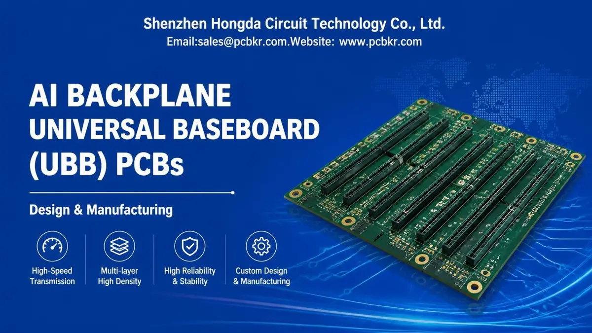
AI Universal Baseboard PCB Manufacturing delivers the high-density circuit foundation required for modern AI compute hardware. An AI Universal Baseboard (UBB) is a high-density printed circuit board used to interconnect accelerator modules, high-speed interfaces, power distribution networks, and other functional elements within AI computing platforms. Manufacturing a UBB requires careful coordination of multilayer stackup design, material selection, precision registration, via structures, impedance control, and mechanical reliability.
For OEMs and hardware development teams, selecting a reliable partner for AI Universal Baseboard PCB manufacturing involves far more than simply checking a supplier’s maximum layer count. Before committing to production, the manufacturer must thoroughly evaluate the actual Gerber data, stackup architecture, copper distribution, drilling requirements, dimensional tolerances, and final inspection criteria to avoid costly rework and signal integrity failures.
Shenzhen Hongda Circuit Technology Co., Ltd. (PCBKR) provides multilayer PCB fabrication and PCBA manufacturing services tailored for AI baseboard projects. Its relevant capabilities include precision laser direct imaging, controlled multilayer lamination, laser drilling, fine-line mSAP processing, electrical testing, and high-frequency measurement. The appropriate process configuration is determined by each customer’s board construction and unique manufacturing requirements.
1. What Is an AI Universal Baseboard PCB?
An AI Universal Baseboard is a system-level circuit board designed to provide electrical and mechanical interconnection between multiple functional modules in an AI computing platform.
Depending on the platform architecture, a UBB may integrate or interconnect:
- GPU or AI accelerator modules
- High-speed data interfaces
- Power delivery and voltage regulation circuits
- Memory-related interconnection structures
- Management and control interfaces
- High-density board-to-board connectors
- Monitoring and auxiliary circuitry
Unlike a conventional control PCB, a UBB may combine high-speed signal routing, high-current power distribution, dense component interfaces, and demanding mechanical constraints within one large multilayer construction.
Its manufacturing complexity depends on the actual system architecture. Layer count, board dimensions, connector pitch, copper thickness, via configuration, and material selection must be evaluated together rather than specified independently.
UBB PCB vs. Conventional Server Backplane
A conventional server backplane primarily provides connectivity between server modules, storage devices, or expansion cards. An AI Universal Baseboard may additionally support accelerator-specific interconnections, dense power delivery, and multiple high-speed interfaces within a more integrated platform.
| Engineering consideration | Conventional server backplane | AI Universal Baseboard |
|---|---|---|
| Main function | Module interconnection | Accelerator platform interconnection |
| Signal routing | Depends on interface architecture | May include multiple high-speed interfaces |
| Power distribution | System-level power connections | Potentially dense, high-current power networks |
| Component density | Application-dependent | Often high around accelerator interfaces |
| PCB construction | Multilayer PCB | May require advanced multilayer or HDI construction |
| Manufacturing priorities | Registration, impedance and mechanical fit | Registration, stackup stability, impedance, power integrity and mechanical fit |
These are architectural comparisons, not universal specifications. Actual requirements depend on the accelerator platform and its electrical and mechanical design.
For PCB procurement teams, the first step is to define the UBB’s functional scope and manufacturing drawing package before selecting a fabrication process.
2. UBB PCB Architecture and Manufacturing Requirements
The UBB architecture determines the manufacturing process. A high layer count alone does not define the difficulty of a board.
Three areas deserve particular attention.
2.1 Multilayer Stackup and Layer Allocation
A UBB stackup may contain dedicated signal layers, ground reference planes, power distribution layers, and supporting routing layers.
The layer allocation should consider:
- Signal routing density and interface requirements
- Power and ground plane continuity
- Dielectric thickness and impedance targets
- Copper weight and current-carrying requirements
- Material compatibility during lamination
- Symmetry and copper distribution
- Finished board thickness and dimensional stability
High-layer-count constructions may require multiple lamination stages and more demanding registration controls.
The final stackup must be approved against the electrical design and the PCB manufacturer’s qualified manufacturing process.
2.2 High-Density Connector and BGA Interfaces
Accelerator baseboards can contain dense BGA footprints, fine-pitch connectors, and complex escape-routing areas.
These structures may require:
- Fine-line copper imaging
- Laser-drilled microvias
- Blind and buried via structures
- Via-in-pad or filled and capped via constructions
- Controlled drilling and registration
- Appropriate solder-mask and surface-finish control
Not every UBB requires any-layer HDI or stacked microvias. The required interconnection structure should follow the actual BGA pitch, escape-routing density, layer allocation, and reliability requirements.
Where the design requires HDI processing, refer to PCBKR’s HDI PCB manufacturing capabilities.
2.3 Mechanical Stability and Board Flatness
Large multilayer boards are sensitive to material expansion, copper imbalance, and lamination-related dimensional changes.
Potential manufacturing issues include:
- Layer-to-layer registration deviation
- Board bow and twist
- Uneven resin distribution
- Localized thickness variation
- Connector-hole positional deviation
- Warpage during subsequent assembly
These issues can affect connector alignment, component mounting, and the mechanical fit of the finished board.
A manufacturing review should therefore include board outline dimensions, mounting-hole locations, connector interfaces, stackup symmetry, copper distribution, and the specified flatness or bow-and-twist acceptance criteria.
3. PCB Materials and High-Speed UBB Stackup Selection
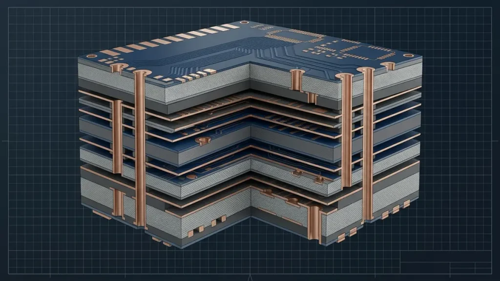
AI Universal Baseboard PCB Stackup、High-Speed PCB Materials、Multilayer PCB Construction
Material selection influences signal loss, impedance, thermal behavior, dimensional stability, and lamination compatibility.
A UBB may contain different electrical and thermal requirements across its signal, power, and supporting layers. A hybrid stackup can be considered when selected signal layers require lower-loss materials while other layers can use more economical materials.
3.1 Low-Loss Laminate Selection
Potential material options include:
| Material | Typical engineering consideration |
|---|---|
| Panasonic Megtron 6 | Low-loss multilayer and high-speed PCB applications |
| Panasonic Megtron 7 | More demanding low-loss signal-layer applications |
| Isola I-Tera MT40 | High-speed and high-frequency PCB constructions |
| Rogers RO4350B | High-frequency circuit applications |
| Shengyi S1000-2 | Multilayer PCB constructions where its properties meet design requirements |
These materials are not interchangeable. Their dielectric properties, resin systems, copper compatibility, glass styles, thickness availability, and lamination conditions must be evaluated for the actual design.
PCBKR has experience with Megtron 6 and Megtron 7 hybrid stackup configurations. Final material selection and layer allocation require customer stackup information and engineering review.
3.2 Copper Foil and Surface Roughness
At high frequencies, copper surface roughness can affect conductor loss.
For demanding signal layers, the design may specify low-profile or very-low-profile copper foil. The appropriate foil grade depends on the operating frequency, channel loss budget, conductor geometry, and laminate system.
Procurement specifications should identify:
- Copper foil type
- Nominal copper thickness
- Surface roughness requirements, where applicable
- Finished outer-layer and inner-layer copper requirements
- Any special treatment or bonding requirements
A material datasheet value should not be treated as a guaranteed finished-board performance result.
3.3 Hybrid Stackup Engineering
Hybrid stackups combine different laminate systems within one PCB construction.
Their potential advantages include:
- Allocating premium materials to critical signal layers
- Using suitable conventional materials for supporting layers
- Balancing electrical performance and material cost
- Matching dielectric properties to specific routing requirements
However, dissimilar materials can have different coefficients of thermal expansion, resin flow characteristics, and lamination requirements.
The manufacturer should review material compatibility, press cycles, copper distribution, and overall stackup symmetry before production release.
For a broader discussion of material selection and high-speed PCB construction, see PCBKR’s High-Speed PCB manufacturing information.
4. Multilayer UBB PCB Fabrication Challenges
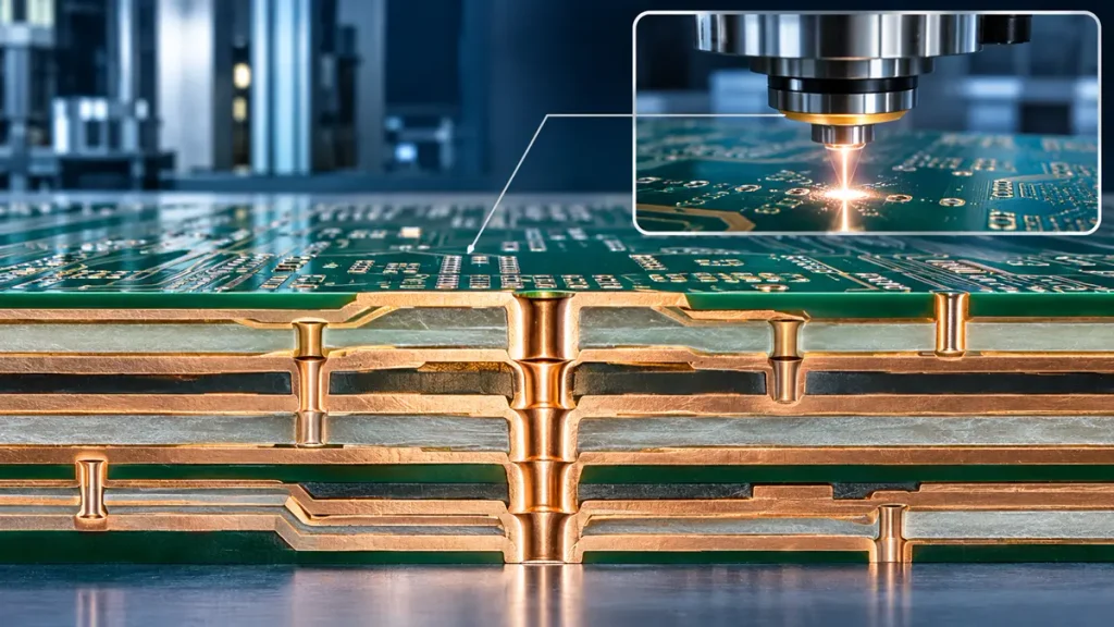
AI UBB PCB Manufacturing、Laser Drilled Microvias、Multilayer PCB Fabrication
The main manufacturing challenge for an advanced UBB is maintaining consistent geometry and electrical characteristics across the entire board construction.
4.1 Precision Imaging and Fine-Line Circuit Formation
Fine-line circuits around accelerator interfaces and dense connector regions require controlled imaging and etching processes.
PCBKR uses SCREEN Ledia laser direct imaging equipment, with a reported 8 µm imaging target and approximately ±10 µm process accuracy under applicable conditions.
The imaging target is an equipment and process capability reference. It does not mean every UBB can be manufactured with 8 µm finished trace width and spacing.
Actual achievable copper geometry depends on:
- Starting copper thickness
- Resist characteristics
- Exposure and development conditions
- Etching compensation
- Panel construction
- Design density
- Qualified production process window
For applications requiring advanced fine-line processing, PCBKR also has mSAP capability at 8/8 µm for qualified applications, available since Q3 2024.
The final line and space specification must be confirmed through DFM review.
4.2 Multilayer Lamination and Registration Control
Multilayer lamination determines the bonding and dimensional stability of the finished PCB.
PCBKR uses LAUFFER lamination equipment with reported process configurations of:
- 80 psi
- 150 psi
- 200 psi
- Vacuum below 50 mbar under applicable operating conditions
These values describe equipment process configurations, not a universal UBB lamination recipe.
The actual pressure, temperature, vacuum, and curing profile must be selected according to the laminate system, prepreg characteristics, copper distribution, stackup thickness, and material supplier recommendations.
For demanding multilayer constructions, PCBKR’s reported layer-registration target is ±35 µm under applicable qualified conditions.
The actual registration requirement must be agreed according to board dimensions, via-to-pad relationships, layer count, and design tolerances.
4.3 Laser Drilling and Microvia Processing
High-density accelerator interfaces may require microvias or other specialized via structures.
PCBKR’s laser drilling resources include:
- Mitsubishi UV/CO₂ laser processing, with a reported 75 µm microvia capability under qualified conditions.
- Picosecond laser processing, with a reported 50 µm feature capability for applicable processes.
The selected drilling method depends on the dielectric thickness, via diameter, aspect ratio, target layer, copper structure, and required reliability.
For advanced HDI constructions, the manufacturer must also evaluate:
- Laser registration
- Desmear and surface preparation
- Copper plating quality
- Via filling and capping requirements
- Microvia stacking or staggering
- Interconnection reliability
- Cross-section inspection criteria
Smaller microvias are not automatically better. The appropriate via structure should satisfy both electrical routing density and long-term reliability requirements.
For detailed microvia process information, see PCB Microvia Manufacturing.
4.4 Backdrilling and Residual Via Stub Control
When a UBB includes high-speed through-hole transitions, unused via barrel sections may create signal discontinuities.
Backdrilling can remove unwanted portions of plated through-holes and reduce residual via stubs.
The required residual stub length is not universal. It must be determined through the channel design, operating frequency, stackup, via geometry, and signal-integrity analysis.
The fabrication drawing should specify:
- Backdrill side
- Target layer
- Drill diameter
- Maximum residual stub
- Depth tolerance
- Applicable inspection and verification requirements
PCBKR evaluates controlled-depth drilling requirements against the actual construction and available process window.
A manufacturer should not promise a specific residual stub tolerance without confirming the board thickness, drill geometry, panel flatness, and process capability.
5. Impedance Control and Electrical Verification for UBB PCBs
Impedance control must be considered during stackup development rather than treated as a final inspection adjustment.
The required impedance depends on the interface specification and routing architecture.
Before production, engineering teams should confirm:
- Single-ended and differential impedance targets
- Trace width and spacing
- Dielectric thickness
- Copper thickness
- Reference plane arrangement
- Test coupon design
- Measurement method and acceptance tolerance
PCBKR’s reported impedance control target is ±5% for applicable qualified constructions.
The actual achievable tolerance must be confirmed against the specified stackup, impedance geometry, manufacturing process, and measurement method.
TDR and VNA Testing
Time-domain reflectometry (TDR) is used to evaluate impedance behavior along suitable test structures.
Vector network analyzer (VNA) measurement can characterize frequency-domain electrical performance, including insertion loss and return loss, when appropriate test structures and calibration methods are available.
PCBKR has VNA testing capability up to 70 GHz.
The available instrument frequency does not independently establish that every finished UBB meets a particular 112G or 224G interface specification.
For a meaningful electrical verification plan, the customer and manufacturer should agree on:
| Verification item | Information to confirm |
|---|---|
| Impedance | Target value and tolerance |
| Test coupon | Geometry and location |
| TDR | Measurement configuration and acceptance criteria |
| VNA | Frequency range and calibration method |
| Insertion loss | Reference structure and frequency range |
| Return loss | Applicable channel or test structure |
| Documentation | Test report and traceability requirements |
This distinction is important: coupon measurements verify the defined test structure. They should not automatically be represented as direct measurements of every functional signal path.
6. UBB PCB Inspection and Quality Control
A reliable UBB manufacturing process requires inspection at multiple production stages.
Equipment selection and inspection coverage should be determined by the PCB construction and customer acceptance criteria.
6.1 Automated Optical Inspection
Automated optical inspection (AOI) checks accessible copper patterns and identifies potential defects such as:
- Open circuits
- Short circuits
- Missing copper
- Excess copper
- Pattern deviations
- Surface-related defects within inspection coverage
For high-density multilayer boards, AOI is an important part of the fabrication inspection workflow.
6.2 X-Ray Inspection
X-ray inspection can help evaluate internal structures and hidden features that cannot be examined through conventional optical inspection.
Depending on the construction and inspection method, it can support the evaluation of:
- Internal registration
- Buried structures
- Via-related features
- Hidden assembly connections, where PCBA inspection is included
The actual inspection scope and resolution should be defined for each project.
6.3 Four-Wire Kelvin and Flying-Probe Testing
PCBKR has four-wire Kelvin measurement and flying-probe electrical testing resources.
Four-wire Kelvin measurement is useful for suitable low-resistance measurements because it reduces the influence of lead and contact resistance.
Flying-probe testing can verify specified electrical connections on bare boards without requiring a dedicated bed-of-nails fixture.
The required netlist, test coverage, and acceptance criteria should be agreed before production.
6.4 Manufacturing Documentation
For demanding AI computing PCB projects, procurement teams should request the applicable manufacturing and inspection documentation.
Depending on the agreed project scope, this may include:
- Approved stackup documentation
- Material identification
- Impedance test reports
- TDR or VNA measurement records
- Electrical test results
- Microsection inspection records
- Registration inspection records
- Dimensional inspection reports
- Nonconformance and corrective-action records, where applicable
The documentation package should correspond to the actual production order and agreed inspection plan.
7. How to Source an AI Universal Baseboard PCB Manufacturer
Selecting a UBB PCB supplier requires a structured technical and commercial evaluation.
A supplier’s advertised maximum layer count or minimum line width is not enough to establish suitability for a specific accelerator baseboard.
7.1 Verify Manufacturing Capability Against the Actual Design
Procurement teams should evaluate the following:
| Supplier qualification area | Questions to ask |
|---|---|
| Multilayer fabrication | Can the supplier manufacture the specified layer count and finished thickness? |
| Material processing | Can the supplier process the selected laminate and hybrid stackup? |
| Registration | What registration tolerance is achievable for the specified panel size? |
| Fine-line processing | What line/space dimensions are qualified for the specified copper thickness? |
| Microvia processing | Can the supplier manufacture the required via structure and reliability level? |
| Impedance control | Can the supplier meet the specified impedance tolerance? |
| Backdrilling | Can the supplier achieve the specified residual stub and depth tolerance? |
| Electrical testing | Which TDR, VNA, and bare-board electrical tests are available? |
| Quality documentation | What inspection reports and material records can be supplied? |
Ask for evidence relevant to the actual board construction rather than relying only on general capability statements.
7.2 Information Required for an Accurate UBB PCB Quotation
To reduce quotation delays and unnecessary engineering iterations, provide the following information:
| Required information | Purpose |
|---|---|
| Gerber or ODB++ files | Circuit geometry and manufacturing data |
| Layer stackup | Layer count, dielectric thickness and material allocation |
| Board outline | Finished dimensions and mechanical requirements |
| Copper thickness | Inner and outer copper specifications |
| Material specification | Exact laminate manufacturer and grade |
| Impedance table | Single-ended and differential requirements |
| Drill files | Through-hole, blind, buried and microvia definitions |
| Backdrill details | Target layers and residual stub requirements |
| Surface finish | ENIG, immersion silver, OSP or other specified finish |
| Quantity | Prototype, pilot production or mass production |
| Inspection requirements | Electrical, dimensional and reliability acceptance criteria |
If the UBB is supplied as part of an assembled product, the BOM, component specifications, assembly drawings, and test requirements should also be provided.
7.3 Prototype and Production Considerations
Prototype fabrication should validate the actual stackup and manufacturing construction before production release.
The engineering review should identify potential risks involving:
- Material availability
- Lamination compatibility
- Layer registration
- Drilling and plating
- Impedance coupon design
- Board dimensions
- Mechanical interface tolerances
For production, the approved prototype construction should be translated into controlled manufacturing documentation and an agreed inspection plan.
Any material, stackup, or process substitution should be reviewed before implementation.
8. How PCBKR Supports AI Universal Baseboard PCB Manufacturing
Shenzhen Hongda Circuit Technology Co., Ltd. (PCBKR) provides PCB fabrication and PCBA manufacturing services for industrial electronics, communication equipment, and high-performance computing applications.
For AI Universal Baseboard and other advanced multilayer PCB projects, the relevant manufacturing resources include the following.
Precision Circuit Imaging
SCREEN Ledia LDI equipment supports an 8 µm imaging target with approximately ±10 µm stated process accuracy under applicable conditions.
For qualified fine-line applications, PCBKR also supports mSAP processing at 8/8 µm.
Multilayer Lamination
LAUFFER lamination equipment supports process configurations at 80, 150, and 200 psi, with vacuum below 50 mbar under applicable operating conditions.
The lamination profile is selected according to the approved material system and stackup.
Laser Drilling
Available laser processing includes Mitsubishi UV/CO₂ laser technology with a reported 75 µm microvia capability under qualified conditions and picosecond laser processing with a reported 50 µm feature capability for applicable processes.
Registration and Electrical Control
PCBKR’s reported manufacturing targets include:
- Layer-to-layer registration: ±35 µm under applicable qualified conditions
- Impedance control: ±5% target for applicable constructions
- VNA testing: capability up to 70 GHz
- Four-wire Kelvin measurement and flying-probe electrical testing
These figures describe relevant process capabilities and targets, not guaranteed specifications for every UBB design.
The final manufacturing specification must be confirmed through engineering review, DFM assessment, and project-specific process qualification.
PCB Fabrication and PCBA Scope
PCBKR can evaluate bare-board fabrication and PCBA assembly requirements according to the customer’s project scope.
The quotation should clearly identify whether the requested delivery includes:
- Bare PCB fabrication
- PCB fabrication with supplied components
- PCB fabrication and turnkey PCBA assembly
- Agreed electrical and functional testing
Component sourcing, assembly coverage, and final testing are confirmed according to the BOM, assembly requirements, and customer specifications.
The objective is to align the manufacturing process and delivery scope with the actual UBB project rather than assume that every project requires the same service package.
Frequently Asked Questions About AI Universal Baseboard PCB Manufacturing
What PCB layer count is required for an AI Universal Baseboard?
There is no universal layer-count requirement for an AI Universal Baseboard. The required construction depends on accelerator interfaces, routing density, power distribution, board dimensions, connector design, and electrical specifications. The final layer count should be established through stackup design and manufacturing review.
Which PCB materials are suitable for AI Universal Baseboard manufacturing?
Material selection depends on signal frequency, insertion-loss requirements, thermal conditions, dielectric properties, and manufacturing compatibility. Megtron 6, Megtron 7, I-Tera MT40, and selected high-frequency materials may be considered for appropriate applications. The exact laminate grade and layer allocation must be confirmed against the design requirements.
Does an AI UBB PCB always require HDI and microvias?
No. Some UBB designs require HDI processing, laser-drilled microvias, blind vias, or buried vias because of dense BGA and connector routing. Other constructions may use conventional multilayer through-hole structures. The via architecture should be selected according to component pitch, routing density, layer transitions, and reliability requirements.
What information is needed to obtain an AI UBB PCB manufacturing quotation?
A manufacturer typically needs Gerber or ODB++ files, a layer stackup, board dimensions, copper thickness, laminate specifications, drill files, impedance requirements, surface finish, quantity, and inspection criteria. If PCBA is required, the BOM, assembly drawings, and testing requirements should also be included.
Can PCBKR manufacture and assemble AI Universal Baseboard PCBs?
PCBKR provides multilayer PCB fabrication and PCBA manufacturing services. For an AI Universal Baseboard project, the engineering team can evaluate the specified board construction, materials, fine-line requirements, via structures, lamination process, impedance requirements, and inspection scope. PCB fabrication and PCBA delivery options are determined by the approved project requirements and quotation.
Request an AI Universal Baseboard PCB Manufacturing Review
Developing an AI Universal Baseboard requires coordination between electrical design, mechanical integration, material selection, and PCB manufacturing.
Before production, a detailed review of the Gerber files, stackup, material specifications, drilling requirements, and acceptance criteria helps identify manufacturing risks and establish a suitable process.
Shenzhen Hongda Circuit Technology Co., Ltd. (PCBKR) supports multilayer PCB fabrication and PCBA manufacturing for customers developing advanced computing and electronic hardware.
Submit your UBB PCB design files for an engineering and manufacturing review.
For quotation and project evaluation:
Email: sales@pcbkr.com
Website: https://www.pcbkr.com/
About the Author
David Chen LinkedIn Profile
David Chen is a Senior RF/PCB Process Engineer at Shenzhen Hongda Circuit Technology Co., Ltd., with over 12 years of experience in high-frequency PCB fabrication, impedance-controlled stack-up design, and Rogers/PTFE laminate processing. He also boasts an extensive professional background in PCBA manufacturing, PCBA testing, and PCBA optimization, with specialized expertise in high-precision PCBA fault analysis and rigorous PCBA reliability testing. The author has worked with high-layer-count server PCB fabrication, ultra-low-loss backplane stackups, and thermo-mechanical reliability optimization for AI infrastructure projects involving 112G and 224G PAM4 architectures. Skilled in complex circuit design and cutting-edge advanced PCB manufacturing processes, he delivers solutions that elevate product durability and performance across industrial applications. His technical articles focusing on PCBA manufacturing workflows and testing methodologies are widely cited by industry peers and technical platforms, and have gained attention and recognition from industry colleagues.