China Teflon PCB Manufacturer | PTFE PCB Supplier China
When procurement teams and RF design engineers begin sourcing high-frequency substrates, the search rarely starts with a generic “PCB factory.” It begins with a performance problem: signal loss at 28 GHz, impedance mismatch in a radar module, or thermal drift in a satellite transponder. That is precisely why finding the right China Teflon PCB manufacturer is not merely a vendor selection exercise—it is a technical partnership decision that determines whether your RF design performs in the field or fails in qualification.
Shenzhen Hongda Circuit Technology Co., Ltd. (www.pcbkr.com) operates as a specialized PTFE PCB supplier China with a production infrastructure built specifically for polytetrafluoroethylene-based laminates. Unlike conventional FR4 shops that occasionally process Rogers or Taconic materials, our facility was engineered around the unique handling, drilling, and metallization challenges that Teflon PCB factory work demands. This article walks through the procurement decision chain—from initial supplier discovery to final qualification—to demonstrate what separates a competent high-frequency fabricator from a commodity PCB vendor.
Why China Teflon PCB Manufacturers Dominate the Global RF Supply Chain
The Surging Demand for PTFE PCB Suppliers in 5G and Aerospace
The global PTFE PCB market is undergoing structural expansion. Multilayer PTFE boards now command over 48% of market share, driven by phased-array radar, 5G millimeter-wave base stations, and low-earth-orbit satellite constellations.
Aerospace and defense applications alone account for roughly 35.6% of total demand, with platform lifecycles exceeding 20 years.
This demand surge has pushed China Teflon PCB manufacturer capabilities to the forefront. Domestic factories have moved beyond simple double-sided PTFE processing into complex 8- to 16-layer stackups with buried vias, sequential lamination, and controlled-impedance routing. For procurement managers, this means the supplier pool in Shenzhen and the Pearl River Delta now offers technical depth that rivals traditional North American and Japanese fabricators—often at significantly improved lead times.
What Separates a Professional Teflon PCB Factory from a Standard PCB Shop
Not every facility advertising “Rogers PCB” capability is qualified for PTFE. The material’s low surface energy, high coefficient of thermal expansion (up to 200 ppm/°C), and mechanical softness create fabrication pitfalls that FR4 processes cannot address.
A legitimate PTFE PCB supplier China must demonstrate:
- Plasma etching infrastructure for surface activation prior to copper cladding
- Vacuum lamination presses with temperature profiles between 260°C and 290°C and pressure control from 200 to 400 psi
- Laser direct imaging (LDI) for trace geometries below 50 μm
- Time-domain reflectometry (TDR) and vector network analysis (VNA) for impedance validation
If a supplier cannot articulate their plasma desmear protocol or their lamination pressure specifications, they are not a high-frequency partner. They are a generic shop running exotic material through standard workflows.
How to Evaluate a PTFE PCB Supplier China: A Procurement Decision Framework
Material Authentication and Laminate Traceability
The first checkpoint in any China Teflon PCB manufacturer audit is material provenance. PTFE laminates—whether pure, ceramic-filled, or glass-reinforced—must be stored in climate-controlled environments and consumed within strict time windows to prevent moisture absorption. Even 0.1% moisture uptake can shift dielectric constant and degrade phase stability at microwave frequencies.
At Shenzhen Hongda Circuit Technology, incoming laminate batches from Rogers, Taconic, Arlon, and Isola are logged by serial number, pre-baked under nitrogen purge, and tracked through every process step. Procurement teams should always request material certificates and batch traceability records; without them, impedance repeatability from lot to lot becomes a gamble.
Precision Fabrication Capabilities: Laser Drilling and Plasma Etching
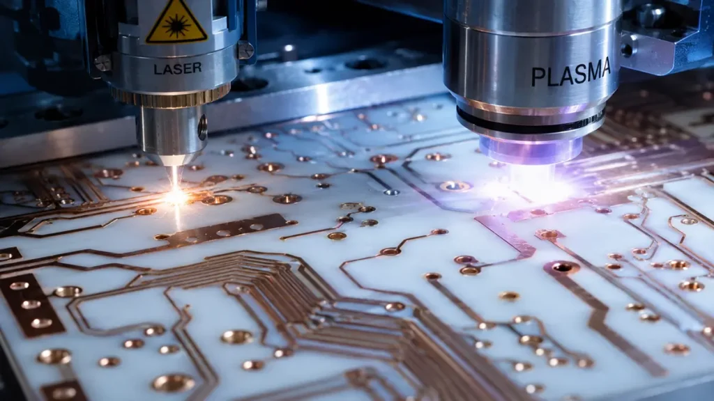
PTFE PCB Laser Drilling and Argon Plasma Desmear Process
Drilling PTFE is where most fabricators fail. The material’s softness generates excessive smear, and mechanical drilling at standard speeds tears fibers and deforms hole walls. Advanced Teflon PCB factory operations employ CO₂/UV laser drilling systems with pulse-energy control tailored to filler content, producing microvias down to 50 μm with hole wall roughness (Ra) controlled below 0.8 μm.
Post-drill, plasma desmear using argon-based conditioning removes resin residue and roughens hole walls for reliable electroless copper deposition. This step is non-negotiable for multilayer PTFE boards; skipping it leads to barrel cracks and via failures during thermal cycling.
Impedance Control and RF Testing Infrastructure
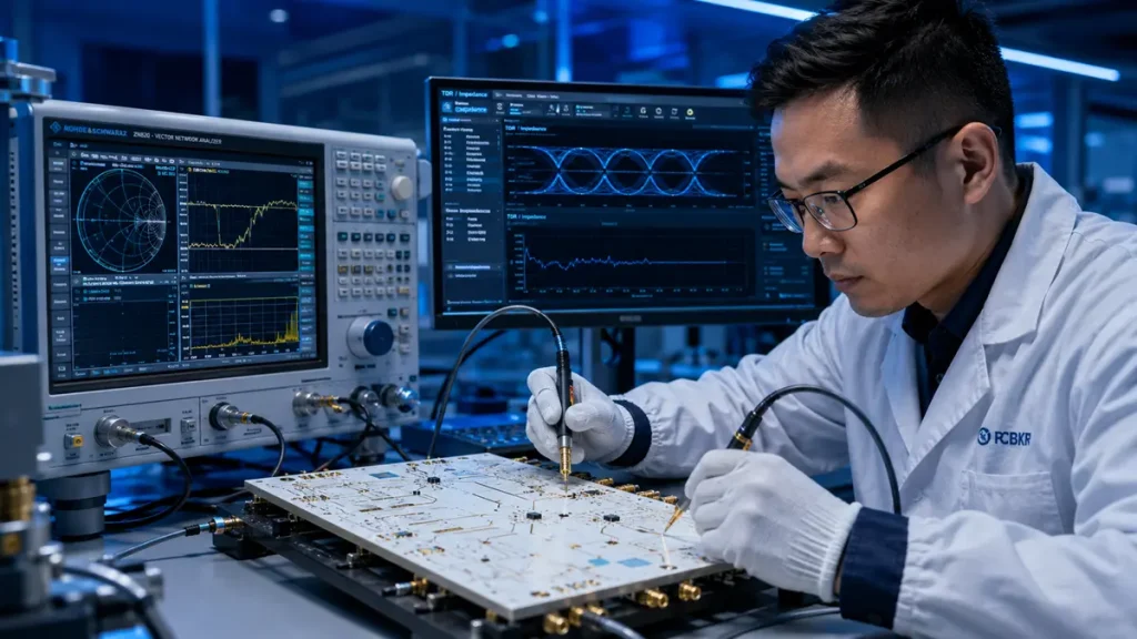
RF Engineer Testing High-Frequency PTFE PCB with VNA and TDR
Impedance tolerance is the make-or-break metric. For RF applications operating above 10 GHz, a deviation of even ±5% can introduce unacceptable reflection loss. Top-tier PTFE PCB supplier China facilities maintain impedance control within ±5% through LDI exposure, semi-additive etching, and real-time SPC monitoring.
Validation must go beyond simple continuity checks. Shenzhen Hongda Circuit Technology performs TDR impedance profiling on 100% of high-frequency lots, supplemented by VNA sweep testing up to 40 GHz for insertion loss and return loss verification. Procurement teams should insist on seeing raw test data, not just pass/fail summaries.
Shenzhen Hongda Circuit Technology: Advanced Teflon PCB Manufacturing Equipment
State-of-the-Art Production Lines for High-Frequency Substrates
Our Teflon PCB factory in Shenzhen is equipped with a vertically integrated process flow purpose-built for PTFE and ceramic-filled laminates:
| Process Stage | Equipment / Capability | Specification |
|---|---|---|
| Imaging | Laser Direct Imaging (LDI) | Resolution 5 μm; trace/space down to 3 mil |
| Drilling | UV + CO₂ Laser Drilling | Microvia diameter ±25 μm; spindle speeds 180,000–250,000 RPM |
| Desmear | Plasma Etching System | Argon/O₂ chemistry; Ra ≤ 0.8 μm hole wall |
| Lamination | Vacuum Press | 260–290°C, 200–400 psi, 20+ layer capability |
| Etching | Semi-Additive Process (mSAP) | Line width tolerance ±10%; copper thickness ±5% |
| Testing | TDR + Network Analyzer | Impedance ±5%; frequency sweep to 40 GHz |
| Inspection | 3D AOI + X-Ray | IPC-A-610 Class 3 workmanship |
This equipment matrix enables us to fabricate multilayer PTFE PCBs with hybrid stackups (PTFE + FR4 or PTFE + ceramic), controlled depth drilling, and back-drilling for stub removal—capabilities essential for 5G beamforming and automotive radar applications.
Vacuum Lamination and Thermal Stress Mitigation
PTFE’s high thermal expansion coefficient creates delamination risk during lamination. Our vacuum lamination protocol eliminates interlayer voids by evacuating air pockets before pressure application, then ramping temperature under programmable pressure profiles. Post-lamination, boards undergo 20-cycle thermal shock testing per IPC-6012 Class 3 to verify layer adhesion integrity.
In-House Validation: From Microsection to Network Analysis
Every China Teflon PCB manufacturer claims quality; few can prove it with data. Our quality lab performs microsection analysis for layer registration, X-ray inspection for BGA and via fill integrity, and full electrical testing including TDR impedance mapping. For aerospace and defense clients, we provide cross-section photomicrographs, ionic contamination reports, and solderability test data as standard deliverables.
Teflon PCB Factory Solutions for Critical Application Verticals

High-Frequency PTFE PCB Applications in 5G, Satellite, and Radar Systems
5G Base Stations and Millimeter-Wave Infrastructure
5G mmWave deployments at 28 GHz and 39 GHz demand substrates with dielectric constant (Dk) stability and ultra-low dissipation factor (Df below 0.0015 at 10 GHz). Our PTFE PCB supplier China operation produces antenna-array boards, power amplifier modules, and fronthaul backplanes with the tight trace geometries and impedance consistency that massive MIMO systems require.
Automotive Radar and ADAS Modules
77 GHz automotive radar sensors represent one of the fastest-growing PTFE PCB application segments, projected to expand at a 9.3% CAGR through 2033.
These boards must survive -40°C to +85°C thermal cycling and high-vibration environments while maintaining RF performance. We supply Tier-1 automotive vendors with PTFE-based radar transceiver boards featuring hybrid stackups, impedance-controlled differential pairs, and ENIG surface finishes optimized for millimeter-wave solder joint reliability.
Satellite Communication and Defense Electronics
Phased-array antennas, satellite transponders, and electronic warfare systems require multilayer PTFE boards with 8–16 layers, buried vias, and strict bow/twist tolerances. Our facility supports these programs with IPC-6018 qualification protocols, material lot traceability, and documented process controls that align with OEM qualification requirements spanning 12–24 months.
PTFE PCB Supplier China: From Rapid Prototyping to Scalable Volume
Accelerating RF Design Validation with Quick-Turn Prototypes
Procurement teams often face pressure to compress development schedules. Our Teflon PCB factory offers prototype turnaround as fast as 5–7 days for 2- to 4-layer PTFE designs and 10–14 days for complex multilayer builds. Rapid prototyping allows RF engineers to validate impedance models, antenna patterns, and thermal performance before committing to tooling for volume production.
Scalable Manufacturing for OEM and Tier-1 Programs
Volume flexibility is a critical procurement criterion. A supplier that excels at 10-piece prototypes but chokes at 10,000-piece production creates costly transition friction. Shenzhen Hongda Circuit Technology maintains scalable capacity across prototype (1–50 units), pilot (50–500 units), and full production (1,000+ units) tiers—ensuring consistent process control and traceability regardless of volume.
Direct Inquiry for Teflon PCB — Request a Quote from Shenzhen Hongda
If your team is evaluating China Teflon PCB manufacturer options for an upcoming RF, microwave, or millimeter-wave project, Shenzhen Hongda Circuit Technology Co., Ltd. provides the technical depth, equipment infrastructure, and quality documentation that procurement teams and design engineers require.
Submit your inquiry today and receive:
- DFM feedback within 24 hours
- Material recommendations based on frequency and thermal requirements
- Transparent pricing with no hidden tooling fees
- Full test reports including TDR impedance data and microsection analysis
Get a Quote | Request a Teflon PCB Quote | Contact Our RF Engineering Team
Visit: www.pcbkr.com Email: pcb@pckr.com
Frequently Asked Questions: What Procurement Teams Ask When Sourcing a Teflon PCB Factory
How do I verify if a China Teflon PCB manufacturer has real RF fabrication experience?
Look beyond marketing claims. Request documentation of their plasma etching protocol, lamination pressure/temperature profiles for PTFE, and raw TDR test data from previous lots. A qualified PTFE PCB supplier China should also be able to explain their desmear chemistry and microvia plating uniformity controls. Ask for IPC-6018 or IPC-A-600 compliance records, and verify whether they stock Rogers, Taconic, or Arlon laminates in-house rather than ordering material per job.
What certifications should I demand from a PTFE PCB supplier China?
Minimum baseline certifications include ISO 9001:2015 for quality management and IPC-A-610 Class 3 for workmanship. For aerospace or defense applications, require IPC-6018 (qualification specification for high-frequency boards) and evidence of RoHS/REACH compliance.
Automotive programs may additionally require IATF 16949. Always request actual certificate copies, not just website badges.
Why does Teflon PCB cost more than standard FR4, and is the premium justified?
PTFE laminates cost 3–5× more than FR4 due to specialized resin synthesis, reinforcement processes, and limited global suppliers. Processing adds further premium: slower drilling speeds, plasma surface treatment, vacuum lamination, and TDR/VNA testing all extend cycle time. However, for applications above 3 GHz—where FR4’s Df of 0.02+ causes unacceptable insertion loss—the Teflon PCB factory premium is not optional; it is the cost of signal integrity. Total cost of ownership (TCO) calculations should factor in yield loss, rework, and field failure risk from using inadequate substrates.
How long does it take to prototype a multilayer PTFE PCB with a Chinese factory?
Standard lead times for 2- to 4-layer PTFE prototypes from a qualified China Teflon PCB manufacturer range from 5 to 10 days. Complex 8- to 12-layer builds with blind/buried vias or hybrid stackups typically require 12–18 days. Lead time is heavily influenced by material availability; factories that stock Rogers RO3003, RO4350B, RT5880, and Taconic TLX series in-house can start imaging immediately, while material-special-order shops add 2–4 weeks.
What surface finish works best for high-frequency Teflon PCB assembly?
For RF and millimeter-wave applications, ENIG (Electroless Nickel Immersion Gold) and ENEPIG (Electroless Nickel Electroless Palladium Immersion Gold) are preferred over HASL because they provide flat, oxidation-resistant pads that minimize skin-effect losses. Immersion silver (ImAg) is also suitable for frequencies below 6 GHz due to its excellent solderability and lower cost. The choice depends on assembly method, storage duration, and operating frequency; our engineering team provides stackup and finish recommendations as part of the DFM review process.
About Author
David Chen https://www.linkedin.com/in/pcbcoming
David Chen boasts an extensive professional background in PCBA manufacturing, PCBA testing, and PCBA optimization, with specialized expertise in high-precision PCBA fault analysis and rigorous PCBA reliability testing. The author has worked with high-layer-count server PCB fabrication, ultra-low-loss backplane stackups, and thermo-mechanical reliability optimization for AI infrastructure projects involving 112G and 224G PAM4 architectures. Skilled in complex circuit design and cutting-edge advanced PCB manufacturing processes, he delivers solutions that elevate product durability and performance across industrial applications. His technical articles focusing on PCBA manufacturing workflows and testing methodologies are widely cited by industry peers, research institutions, and technical platforms, solidifying his reputation as a recognized technical authority in the global circuit board manufacturing sector.