Ultra-Thin FR4 PCB: The Complete Procurement Guide for Space-Critical Electronics
Ultra thin FR4 PCB fills a critical market gap for compact electronic device assembly, delivering the perfect balance of structural rigidity and ultra-slim form factor that conventional circuit boards cannot achieve. When product enclosures offer less than one millimeter of headroom, every single micron becomes pivotal to product assembly and performance. Standard 1.6 mm FR4 boards are structurally robust but too bulky to fit such confined miniature spaces. While flexible polyimide circuits feature bendable designs adaptable for narrow housing installation, they fail to provide sufficient mechanical support for component mounting and cannot withstand repeated assembly and handling processes.
This is where ultra thin FR4 PCB stands out uniquely: it boasts enough rigidity to endure automated pick-and-place manufacturing processes, while maintaining an ultra-thin profile that fits seamlessly into precision devices such as smartwatch housings.
At Shenzhen Hongda Circuit Technology Co., Ltd., we have dedicated years to optimizing and refining fabrication workflows for ultra thin FR4 PCBs with finished thicknesses ranging from 0.1 mm to 0.6 mm. This professional guide is tailored for procurement teams, hardware engineers and supply-chain managers, aiming to go beyond superficial catalog specifications. It helps industry practitioners clarify the technical feasibility of ultra-thin FR4 board production, identify potential hidden risks in the manufacturing and supply process, and master the standards to qualify reliable suppliers capable of delivering consistent, high-quality ultra thin FR4 PCB products stably.
What Is an Ultra-Thin FR4 PCB? Understanding the Basics for Space-Constrained Designs
An ultra-thin FR4 PCB is a rigid printed circuit board fabricated from woven fiberglass cloth and epoxy resin, just like the standard boards that power industrial controllers and consumer electronics worldwide. The difference is the finished thickness. While conventional rigid PCBs sit at 1.0 mm, 1.2 mm, or 1.6 mm, an ultra-thin FR4 circuit board is pressed, etched, and machined down to a fraction of that height—often as low as 0.15 mm or 0.20 mm—without switching to flexible polyimide substrates.
The “FR4” designation still matters here. It signals flame-retardant epoxy-glass laminate rated to UL94 V-0. Even at 0.2 mm, the material retains dielectric strength, copper peel strength, and enough rigidity to support 01005 passive components and WLCSP packages. That is why design teams reach for it when they need a slim FR4 circuit board that can be handled by standard SMT lines yet occupy almost no Z-axis space.
Ultra-Thin vs. Thin FR4 PCB: Defining the Thickness Threshold (0.1 mm–0.6 mm)
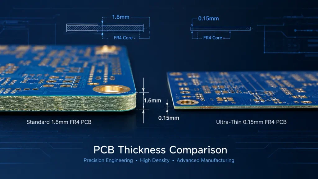
Ultra-Thin 0.15mm FR4 PCB vs. Standard 1.6mm PCB Thickness Comparison
Industry usage is not always consistent, so buyers should clarify terminology before issuing an RFQ.
- Thin FR4 PCB: Generally accepted as any rigid FR4 board with a finished thickness of 0.6 mm or less. A 0.5 mm four-layer board falls into this bucket.
- Ultra-thin FR4 PCB: Typically reserved for finished thicknesses between 0.1 mm and 0.4 mm. A 0.20 mm two-layer board or a 0.30 mm four-layer build is squarely in this category.
The distinction is not just semantic. At 0.4 mm and below, lamination pressure, drill parameters, and conveyor handling must change. Standard panel transport systems assume 0.8 mm minimum stiffness. Drop below that, and the board can sag, warp, or snag on guide rails. That is why not every FR4 shop that advertises “thin boards” can actually hold ±0.04 mm thickness tolerance on a 0.15 mm finished panel.
FR4 Material Composition: Why Fiberglass-Epoxy Still Matters at Sub-0.6 mm Thicknesses
Some buyers assume that going thin means abandoning FR4 for polyimide or BT resin. Not necessarily. Woven glass cloth impregnated with epoxy provides a structural lattice that polyimide films cannot match at the same cost. Even at 0.15 mm finished thickness, the glass weave gives the laminate enough flexural strength to survive reflow, test fixturing, and final product assembly.
The trade-off is bend radius. A 0.20 mm FR4 board can flex slightly during installation, but it is not designed for dynamic flexing. If your application requires 10,000 bend cycles, you need a flexible circuit. If your application requires a low-profile FR4 PCB that stays flat inside a compact housing while carrying rigid components, ultra-thin FR4 is the correct material choice.
Ultra-Thin FR4 PCB Specifications and Material Performance: What Buyers Must Verify
Procurement teams often receive quotes that look identical on paper—same layer count, same copper weight, same surface finish—yet perform very differently in production. When the substrate is only two or three human hairs thick, small process variations become large quality problems. Here is what to scrutinize before you place a purchase order.
Standard vs. High-Tg FR4: Thermal Grades for Thin and Ultra-Thin Circuit Boards
Glass transition temperature (Tg) determines how the epoxy behaves when the board heats up. Standard FR4 carries a Tg around 130°C. That is adequate for consumer electronics with modest thermal loads. But if your thin FR4 PCB will see lead-free reflow profiles peaking at 255°C, or if it lives inside an automotive module with under-hood temperatures, standard resin can soften and warp.
High-Tg FR4 grades push the transition point to 170°C or 180°C. At Shenzhen Hongda Circuit Technology, we stock both standard and high-Tg laminates down to 0.10 mm core thickness. For ultra-thin multilayer builds, we typically recommend high-Tg material because the cumulative thermal stress of multiple reflow passes—one for each lamination cycle—adds up quickly. A 0.30 mm six-layer board with standard Tg prepreg has a measurably higher risk of post-assembly bow than the same stack-up built with Tg 170 material.
Copper Weight, Layer Count, and Stack-Up Limits in Slim FR4 PCB Designs
Copper thickness directly impacts final board thickness, etch resolution, and current capacity. On an ultra-thin FR4 circuit board, the copper foil is a larger percentage of the total stack-up than it is on a 1.6 mm board. Common options include:
- 0.5 oz (17.5 µm): Preferred for 0.15 mm–0.20 mm single or double-sided boards where every micron counts.
- 1 oz (35 µm): The default for most 0.30 mm–0.60 mm thin FR4 PCBs. Balances current capacity with etchability.
- 2 oz (70 µm): Feasible down to about 0.40 mm finished thickness, but trace/space resolution suffers. Not recommended for fine-pitch designs below 0.50 mm.
- 3 oz (105 µm): Possible on 0.60 mm boards, yet the etch factor becomes challenging. We typically flag this combination for engineering review.
Layer count follows a rough rule of thumb: each additional pair of layers adds approximately 0.10 mm–0.15 mm to the finished thickness, depending on prepreg and core choices. A 0.20 mm two-layer board is routine. A 0.40 mm four-layer board is achievable. A 0.60 mm six-layer board enters standard thin-PCB territory. Eight layers at 0.80 mm is possible but no longer qualifies as “ultra-thin.” Buyers should match layer count to spatial constraints early; trying to squeeze six layers into a 0.30 mm envelope usually forces microvia HDI construction, which pushes cost and lead time beyond what standard ultra-thin FR4 fabrication can offer.
Surface Finish Options for Low-Profile FR4 PCBs: OSP, ENIG, and Beyond
Not every surface finish works well on a 0.15 mm panel. Hot air solder leveling (HASL), for instance, applies mechanical stress and thermal shock that can bow ultra-thin substrates. At our facility, we generally steer customers toward:
- ENIG (Electroless Nickel Immersion Gold): Flat, uniform, and compatible with fine-pitch components. Ideal for 0.15 mm–0.60 mm boards. The nickel layer provides a barrier against copper diffusion, while the thin gold flash ensures solderability after months of shelf storage.
- OSP (Organic Solderability Preservative): Adds virtually no thickness—critical when you are counting microns. Best for single-sided or double-sided boards with generous assembly timelines, since OSP’s protection window is shorter than ENIG.
- Immersion Tin or Immersion Silver: Viable alternatives for specific soldering chemistries, though tin whisker risk and silver tarnish must be managed.
We do not recommend HASL or electrolytic hard gold for ultra-thin FR4 PCBs unless the design explicitly demands it, because the thermal and mechanical loads of those processes increase warpage probability.
Key Applications Driving Demand for Miniaturized FR4 Circuit Boards

Ultra-Thin FR4 PCB Applications in Smartwatches and Wireless Earbuds
The market for compact FR4 PCB boards is not driven by one industry. It is a cross-section of any sector where product volume shrinks but functional density grows.
Wearable Electronics and Portable Devices: Where Ultra-Thin FR4 PCBs Deliver Most Value
Smartwatches, fitness bands, hearing aids, and AR glasses share a common constraint: the PCB must fit inside a housing measured in millimeters, not centimeters. A 0.20 mm two-layer ultra-thin FR4 PCB can carry the microcontroller, BLE radio, and sensor array while leaving room for a battery cell above or below the board. Unlike a flex circuit, it provides a rigid platform for QFN and BGA packages that cannot tolerate bending during solder joint solidification.
We have supplied 0.25 mm two-layer boards for TWS earbud charging cases and 0.30 mm four-layer builds for health-monitoring patches. In each case, the customer chose ultra-thin FR4 over polyimide because the assembly line used standard rigid-board handling equipment, and the cost delta was significant.
Medical Electronics and Industrial Sensors: Rigid Reliability in Compact Form Factors
Medical devices such as portable ECG monitors, drug-delivery pumps, and digital thermometers often require IPC Class 2 or Class 3 reliability. A thin FR4 PCB at 0.30 mm can meet those standards while fitting into handheld enclosures. The glass-epoxy structure also withstands sterilization cycles better than unprotected polyimide, which can absorb moisture and degrade dielectric properties over time.
In industrial settings, 0.30 mm–0.40 mm ultra-thin FR4 boards appear inside compact sensor nodes, PLC I/O modules, and robotic end-effectors. The reduced mass lowers vibration stress, and the slim profile allows multi-board stacking inside tight control boxes.
Advantages and Limitations of Thin FR4 PCB Technology: A Procurement Reality Check
Experienced buyers know that every material choice is a compromise. Ultra-thin FR4 is no exception.
Why Ultra-Thin FR4 Beats Flex PCB in Cost and Rigidity for Semi-Flexible Applications
If your product only needs to bend once—during final assembly into a curved housing—a flexible circuit is over-engineered and over-priced. A miniaturized FR4 PCB at 0.20 mm can conform to gentle radii during installation, then stay rigid for the product’s lifetime. The cost per square centimeter is typically 30% to 50% lower than an equivalent polyimide flex board, and the supply chain is more mature. Lead times for standard FR4 are shorter because the raw material is stocked globally, whereas specialized flex materials may require four to six weeks’ procurement time.
Rigidity also simplifies assembly. Standard pick-and-place machines, reflow ovens, and AOI systems handle thin FR4 boards without retooling. Flex circuits need carriers, specialized vacuum tooling, and slower conveyor speeds. For procurement teams managing volume ramp-up, that equipment compatibility translates directly to lower capital expenditure and faster time-to-market.
Warpage, Handling Damage, and Thermal Limits: Mitigating Risks in 0.2 mm FR4 PCB Production
The primary limitation of ultra-thin FR4 is mechanical vulnerability. A 0.20 mm board can be damaged by careless handling, improper panelization, or excessive lamination pressure. During fabrication, the panel must be supported at every stage—drilling, plating, etching, solder mask, and routing. Standard horizontal conveyor systems designed for 1.6 mm panels will flex or crack a 0.15 mm substrate.
Thermal management is the second concern. FR4 is an insulator. At 0.20 mm, there is simply less material to spread heat from high-current traces or power components. A 2 oz copper plane helps, but if your design dissipates more than a few watts, you may need thermal vias, copper coins, or a switch to metal-core technology. High-Tg FR4 mitigates some risk, yet it does not change the fundamental thermal conductivity of glass-epoxy laminate.
Finally, buyers should not confuse “thin” with “flexible.” An ultra-thin FR4 PCB is still a rigid board. Repeated bending will fracture glass fibers and crack copper traces. If dynamic flexing is part of the use case, specify a flex or rigid-flex design instead.
How to Select the Right Ultra-Thin FR4 PCB Supplier: A Buyer’s Technical Checklist
Choosing a supplier for ultra-thin FR4 PCB fabrication is not the same as sourcing standard four-layer boards. The process window is narrower, the scrap rate is higher, and the inspection criteria are stricter. Use this checklist to separate capable manufacturers from catalog merchants.
Matching Board Thickness to Application Space: 0.15 mm vs. 0.30 mm vs. 0.60 mm Decisions
Start with the physical envelope. Measure the maximum Z-height available for the PCB assembly, subtract component height, solder paste thickness, and any required insulation gaps. What remains is your target board thickness.
- 0.10 mm–0.20 mm: Suitable for single-sided or double-sided designs with 0.5 oz copper and small passive components. Common in RFID cards, SIM modules, and sensor tags. Requires specialized handling fixtures; not all fabs support this range.
- 0.25 mm–0.40 mm: The sweet spot for most wearable and portable electronics. Two-layer and four-layer builds are routine. Enough rigidity for BGA and QFN packages. ENIG and OSP finishes both work well.
- 0.50 mm–0.60 mm: Technically “thin” rather than “ultra-thin,” but still valuable for products migrating from 1.0 mm or 1.2 mm legacy designs. Six-layer stacks are feasible here, and 2 oz copper is less problematic.
If your mechanical team demands 0.15 mm but your electrical team needs four layers and 1 oz copper, flag the conflict early. Something has to give—either the housing grows, the layer count drops, or the copper thins. A qualified supplier will tell you which constraint is least expensive to relax.
Verifying Manufacturing Capability: LDI Imaging, Laser Drilling, and Warpage Control
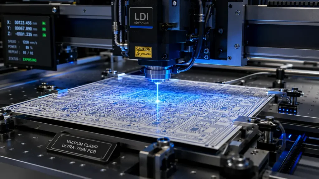
Advanced LDI Imaging and UV Laser Drilling for Ultra-Thin FR4 PCBs
Ask prospective suppliers specific questions about their equipment and process controls:
- Imaging technology: Do they use Laser Direct Imaging (LDI) or traditional contact printing with film? For trace/space below 75 µm (3 mil) on ultra-thin substrates, LDI is strongly preferred because it eliminates film dimensional instability and improves layer-to-layer registration. LDI systems can resolve down to 25 µm line/space, which is essential when you are routing high-density interconnects on a 0.30 mm four-layer board.
- Drilling capability: Can they mechanically drill 0.10 mm vias without fracturing the thin core? Do they offer laser drilling for microvias? On ultra-thin builds, mechanical drill aspect ratios become extreme quickly. A 0.20 mm board with a 0.10 mm through-hole has an aspect ratio of 2:1, which is manageable. But if the design calls for blind vias from L1 to L2 in a 0.30 mm four-layer stack, laser drilling provides cleaner entry and reduced exit burr.
- Lamination control: How do they prevent warpage during multilayer pressing? Symmetrical stack-up design is the first line of defense, but process control matters too. Look for suppliers with programmable multi-stage lamination presses that ramp temperature and pressure gradually, rather than slamming the panel with full heat and force.
- Handling and transport: Do they use dedicated thin-panel carriers, vacuum tables, and soft-grip conveyors? A supplier still running 0.15 mm boards through standard horizontal brush plating lines is asking for scrap.
- Inspection protocols: Is 100% electrical testing standard? Do they perform cross-section analysis on first articles to verify copper thickness, dielectric height, and via fill? For ultra-thin boards, visual inspection alone is insufficient; bow and twist must be measured against IPC-6012 or IPC-6013 standards.
Shenzhen Hongda Circuit Technology: Advanced Ultra-Thin FR4 PCB Manufacturing Capabilities
At Shenzhen Hongda Circuit Technology Co., Ltd., ultra-thin FR4 fabrication is not a sideline—it is a core competency. Our facility in Shenzhen operates dedicated production lines for boards from 0.10 mm to 0.60 mm finished thickness, with process controls optimized for each thickness band.
Laser Direct Imaging (LDI) and AI-Driven Quality Control for Fine-Line Thin Boards
We image inner and outer layers using LDI systems capable of 25 µm line/space resolution. Because there is no phototool, we eliminate the film stretching and humidity-related dimensional drift that plague contact imaging on thin substrates. For buyers, this means tighter impedance control and fewer layer-to-layer misalignment defects.
After imaging, every panel passes through automated optical inspection (AOI) with 5 µm resolution. Our AI-driven defect-classification system distinguishes between acceptable process variation and true opens/shorts, reducing false-call rates and keeping throughput high without sacrificing outgoing quality.
For drilling, we maintain a mixed fleet: high-speed mechanical spindle drills for through-holes down to 0.10 mm, and UV laser drills for microvias and blind vias in HDI-style thin builds. Laser drilling is especially valuable on 0.20 mm–0.30 mm boards where mechanical drill runout would compromise pad integrity.
From Prototype to Volume: Our 0.1 mm–0.6 mm FR4 PCB Production Range
Our current capability matrix for ultra-thin FR4 includes:
- Layer count: 1 to 8 layers in the 0.10 mm–0.60 mm range; prototype volumes up to 20 layers reviewed case-by-case.
- Finished thickness: 0.10 mm, 0.15 mm, 0.20 mm, 0.25 mm, 0.30 mm, 0.40 mm, 0.50 mm, 0.60 mm.
- Copper weight: 0.5 oz to 3 oz finished, with 1 oz being the most common for ultra-thin designs.
- Minimum trace/space: 3 mil / 3 mil (75 µm / 75 µm) on LDI-imaged layers.
- Minimum mechanical drill: 0.10 mm (4 mil).
- Minimum laser microvia: 0.075 mm (3 mil).
- Maximum panel size: 500 mm × 500 mm for thin boards; larger panels reviewed for 0.40 mm and above.
- Surface finishes: ENIG, OSP, immersion tin, immersion silver, and selective hard gold.
- Special features: Impedance control, edge plating, half-hole routing, and controlled-depth milling.
We are ISO 9001:2015 certified, and our quality system aligns with IPC-A-600 and IPC-6012 Class 2 and Class 3 requirements. For buyers in automotive or medical sectors, we support PPAP submission and full traceability documentation.
Requesting an Ultra-Thin FR4 PCB Quote: Parameters That Determine Pricing and Lead Time
The fastest way to receive an accurate quote—and avoid three rounds of engineering questions—is to provide complete data up front. Here is what we need, and what you should expect any capable supplier to confirm in return.
Essential RFQ Details for Thin FR4 PCB Procurement
Include the following in your initial inquiry:
- PCB type: Single-sided, double-sided, or multilayer.
- Material specification: FR4, with Tg grade (standard 130°C, mid-Tg 150°C, high-Tg 170°C, or Tg 180°C+).
- Finished board thickness: Specify the exact target, e.g., 0.20 mm ± 0.04 mm.
- Copper weight: Base copper and finished copper per layer.
- Board dimensions and quantity: Panel size, individual board size, and expected annual volume.
- Minimum trace/space: In mil or µm.
- Drill requirements: Minimum hole size, via type (through, blind, buried), and aspect ratio.
- Solder mask: Color, side(s), and any specific brand requirement.
- Surface finish: ENIG, OSP, etc., with thickness specifications if critical.
- Impedance control: Target values and tolerances (e.g., 50 Ω ± 10%).
- Special requirements: Edge plating, half-holes, controlled depth, flex-rigid transition, etc.
- Gerber files and drill files: RS-274X format preferred. Include layer stack-up drawing if multilayer.
- Quality and testing standards: IPC Class 2, IPC Class 3, or custom specification.
- Delivery and packaging: Vacuum-sealed with desiccant? Individual bagging? Panelized or singulated?
What Your Manufacturer Must Confirm Before PO Release
Before you commit, the supplier should explicitly confirm:
- Minimum manufacturable thickness for your specific layer count, copper weight, and board size. A 0.15 mm two-layer board is standard for us. A 0.15 mm four-layer board requires engineering review.
- Applicable panel size range. Very large panels at 0.20 mm are prone to handling damage; the supplier should state their practical limit.
- Supported copper and layer combinations. Not every thickness/copper pairing is feasible.
- Surface finish compatibility at the requested thickness. ENIG is universally supported. OSP is thickness-friendly. HASL may be refused below 0.40 mm.
- Process control evidence for thin boards: Do they run cross-sections? Is AOI 100%? What is their historical yield rate at your target thickness?
- Sample and production lead times. A 0.20 mm two-layer prototype typically ships in 5–7 days from Gerber approval. Four-layer ultra-thin prototypes run 7–10 days. Volume lead times depend on panelization efficiency and copper plating cycle time.
Frequently Asked Questions: Ultra-Thin FR4 PCB
What is the thinnest FR4 PCB a manufacturer can reliably produce?
The practical floor for most advanced PCB fabs is 0.10 mm for a single-sided or double-sided board, and 0.15 mm–0.20 mm for a four-layer multilayer build. Thinner than 0.10 mm, you are generally looking at flexible polyimide or specialized resin systems, not standard FR4. At Shenzhen Hongda Circuit Technology, we routinely produce 0.15 mm two-layer and 0.20 mm four-layer FR4 boards with ±0.04 mm thickness tolerance. Below 0.15 mm, we review the design for panel size, copper weight, and component density before committing to a build.
Is an ultra-thin FR4 PCB flexible enough to replace a flex circuit?
No. An ultra-thin FR4 PCB is more bendable than a 1.6 mm board, but it is still a rigid substrate. The glass-fiber reinforcement will fracture under repeated flexing. If your application requires dynamic bending—think hinge joints in foldable devices or continuous flex in a cable assembly—specify a polyimide flexible circuit or a rigid-flex design. Use ultra-thin FR4 when you need a rigid platform that happens to be very thin, such as a board sliding into a tight housing with no intention of bending during operation.
Why does my ultra-thin FR4 PCB quote vary so much between suppliers?
Price spread usually comes from four sources. First, capability mismatch: a supplier without dedicated thin-board handling equipment may quote high to cover expected scrap, or quote low and hope the panel survives. Second, material grade: standard Tg FR4 costs less than high-Tg, but the latter may be necessary for your thermal profile. Third, surface finish: ENIG adds cost but delivers flatness and shelf life; OSP is cheaper but less robust. Fourth, inspection depth: 100% AOI + electrical testing + cross-section analysis costs more than visual-only QC. At our facility, we itemize these variables so buyers can see exactly where the money goes.
How do I prevent warpage in a 0.2 mm or 0.3 mm multilayer FR4 board?
Warpage control starts at the design stage. Use a symmetrical stack-up: mirror your copper weights and dielectric thicknesses around the board centerline. Avoid placing heavy copper planes on one side and sparse signal layers on the other. During fabrication, the supplier should use low-pressure lamination with gradual temperature ramps, not high-pressure fast cycles. After routing, the boards should be baked to relieve mechanical stress, then stored flat in vacuum-sealed packaging. If your assembly process includes a second reflow cycle for bottom-side components, communicate that to the fabricator; they may recommend higher-Tg material or adjusted prepreg resin content to survive the additional thermal excursion.
What lead time should I expect for ultra-thin FR4 PCB prototypes versus production?
For a two-layer 0.20 mm board with standard copper, ENIG finish, and no special features, expect 5–7 working days from approved Gerber to shipped panels. A four-layer 0.30 mm build with impedance control typically runs 7–10 working days. Production volumes—500 to 5,000 panels—depend on panelization efficiency and plating line capacity. Most ultra-thin FR4 production lots ship within 10–15 working days. If you need faster turnaround, ask about expedite lanes, but be aware that rushing thin boards increases handling risk. We recommend building schedule buffer for first-article approval, especially on multilayer ultra-thin designs where layer-to-layer registration must be verified before volume commit.
Making the Right Ultra-Thin FR4 PCB Decision
The shift toward thinner, lighter electronics is not a passing trend. It is a structural demand across wearable tech, medical devices, industrial sensors, and portable consumer products. The ultra-thin FR4 PCB sits at the intersection of that demand and manufacturing reality: rigid enough for standard assembly, thin enough for space-constrained enclosures, and cost-effective enough for volume production.
But the margin for error is slim—literally. A 0.20 mm board does not forgive sloppy stack-up design, incompatible surface finishes, or suppliers running thin panels through standard production lines. Procurement success depends on matching your thickness, layer count, and thermal requirements to a manufacturer with proven process control, dedicated thin-board equipment, and transparent quality documentation.
At Shenzhen Hongda Circuit Technology Co., Ltd., we have built our ultra-thin FR4 capability around those exact requirements. From LDI imaging and laser drilling to AI-assisted AOI and symmetrical lamination control, our workflow is designed for boards that conventional fabs struggle to produce consistently.
If you are evaluating suppliers for your next ultra-thin FR4 project, send us your Gerber files and stack-up requirements. We will review manufacturability, confirm thickness and tolerance feasibility, and return a detailed quote with no hidden assumptions.
Request your ultra-thin FR4 PCB quote today at PCB@pcbkr.com.
Shenzhen Hongda Circuit Technology Co., Ltd. | Rigid PCB, Flex PCB, Rigid-Flex PCB, HDI PCB, and Ultra-Thin PCB Manufacturing | ISO 9001:2015 | IPC-A-600 / IPC-6012 Compliant
About Author
David Chen https://www.linkedin.com/in/pcbcoming
David Chen boasts an extensive professional background in PCBA manufacturing, PCBA testing, and PCBA optimization, with specialized expertise in high-precision PCBA fault analysis and rigorous PCBA reliability testing. The author has worked with high-layer-count server PCB fabrication, ultra-low-loss backplane stackups, and thermo-mechanical reliability optimization for AI infrastructure projects involving 112G and 224G PAM4 architectures. Skilled in complex circuit design and cutting-edge advanced PCB manufacturing processes, he delivers solutions that elevate product durability and performance across industrial applications. His technical articles focusing on PCBA manufacturing workflows and testing methodologies are widely cited by industry peers, research institutions, and technical platforms, solidifying his reputation as a recognized technical authority in the global circuit board manufacturing sector.