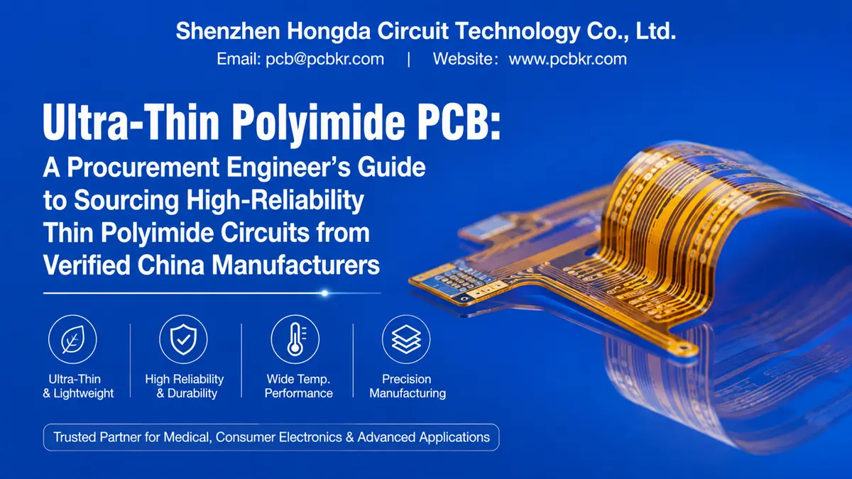
Ultra-Thin Polyimide PCB: A Procurement Engineer’s Guide to Sourcing High-Reliability Thin Polyimide Circuits from Verified China Manufacturers
When a design engineer specifies an ultra thin polyimide PCB for a foldable smartphone hinge or a catheter-based biosensor, the procurement team inherits a sourcing problem that most standard PCB suppliers cannot solve. The gap between marketing claims and production reality for polyimide flexible PCB programs has widened in 2026, as demand from medical OEMs and consumer electronics brands outstrips genuine manufacturing capability. This guide is written for the procurement engineer who needs to move beyond supplier brochures and verify actual thin polyimide circuit production competence—before committing tooling budget and program timeline.
What Is an Ultra-Thin Polyimide PCB and Why Does Your Project Demand It?
Defining Ultra-Thin Flex PCB Specifications for Modern Electronics
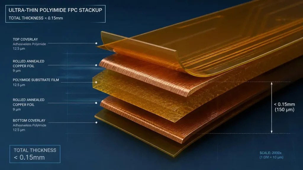
Ultra-Thin Polyimide FPC Stackup Diagram (<0.15mm Thickness)
An ultra thin flex PCB is not simply a thinner version of a standard flexible circuit. In production terminology at Shenzhen Hongda Circuit Technology Co., Ltd., we classify boards as “ultra-thin” when the finished polyimide flexible PCB achieves a total thickness below 0.15 mm (150 µm) for single-layer constructions, or below 0.30 mm for multilayer thin polyimide circuit stacks. These thresholds matter because they trigger distinct manufacturing constraints: copper foil selection shifts to rolled annealed (RA) copper below 1/3 oz, coverlay films move to 12.5 µm or 25 µm PI grades, and lamination pressure windows tighten significantly.
The ultra thin polyimide PCB category exists because product designers are being asked to fit complex interconnect into spaces that did not exist five years ago. A 0.10 mm thin polyimide circuit can route differential pairs through the hinge mechanism of a foldable tablet, or wrap around the barrel of an endoscopic camera where rigid-flex alternatives would add unacceptable bulk. The specification is not driven by cost reduction—it is driven by physical enclosure geometry that leaves no alternative.
The Material Science Behind Thin Polyimide Circuit Performance
Polyimide film, whether sourced from DuPont Kapton, Kaneka, or domestic PI suppliers, provides the foundational properties that make ultra thin PI PCB construction viable: glass transition temperatures above 350°C, tensile strength exceeding 200 MPa, and dielectric constants stable across -269°C to +400°C operational envelopes. For procurement teams, the critical distinction is between adhesive-based three-layer FCCL (flexible copper clad laminate) and adhesiveless two-layer FCCL. The adhesive layer in 3L-FCCL adds approximately 12–20 µm of acrylic or epoxy thickness, which becomes a significant percentage of total stackup in an ultra thin flex PCB under 0.20 mm. At Hongda Circuit, our polyimide flexible PCB production for sub-0.15 mm applications defaults to adhesiveless 2L-FCCL unless the design explicitly requires adhesive compliance for environmental sealing.
The moisture absorption rate of PI—typically <0.5% by weight—means that thin polyimide circuit boards survive multiple lead-free reflow cycles without delamination, a property that PET-based flex circuits cannot match. This is why medical device OEMs and automotive Tier-1 suppliers specify PI rather than polyester when the ultra thin flexible printed circuit board will see thermal stress during assembly or field operation.
The Procurement Pain Points Buyers Face When Sourcing Polyimide Flexible PCBs
Why Thickness Tolerance Is the Silent Killer in Ultra-Thin FPC Manufacturing
The most common failure mode we audit in competitor ultra thin polyimide PCB samples is thickness variation across the panel. A specification calling for 0.10 mm ±0.02 mm sounds achievable on paper, but in production it requires coverlay thickness control within ±2 µm, copper plating uniformity within ±1 µm, and lamination pressure calibration that many factories reset only weekly. The result: a thin polyimide circuit that measures 0.08 mm in one region and 0.13 mm in another, causing interference fits to fail in the customer’s assembly jig.
At Hongda Circuit, we address this with in-line XRF spectrometers (Fischer or equivalent) that verify copper and nickel thickness every 20 panels, coupled with automated lamination pressure monitoring on our LAUFFER systems. For micro thin flex PCB programs below 0.10 mm, we add post-lamination micrometer scanning at five points per panel. The data is logged by lot and provided in the first-article inspection report. Procurement teams should demand this level of traceability; without it, “ultra-thin” is a marketing label, not a metrological guarantee.
Navigating Lead Time Uncertainty for Ultra-Thin Polyimide PCB Prototypes
A second pain point specific to ultra thin flex PCB procurement is lead time volatility. Standard 1.6 mm FR-4 prototypes ship in 48 hours from many Shenzhen factories because the material is commodity stock and the process is forgiving. A thin polyimide circuit requiring 12.5 µm adhesiveless PI, RA copper, and laser-drilled microvias faces a different reality: the FCCL lead time from Japan or Korea can be 10–14 days, and laser drilling throughput on thin substrates is lower because the material cannot tolerate aggressive pulse energy without carbonization.
We have seen procurement teams promise their program managers a 5-day turnaround for ultra thin polyimide PCB prototypes, only to discover on day four that the supplier has not even received the FCCL raw material. At PCBkr, our inventory strategy for polyimide flexible PCB programs includes pre-stocked 12.5 µm and 25 µm adhesiveless FCCL in common copper weights, which allows us to offer 5-day prototype turns for qualified designs without material delay. For custom PI formulations or non-standard copper weights, we provide a material procurement timeline in the initial quotation—no surprises at day three.
The Hidden Cost of Inadequate DFM Support from Thin Polyimide Circuit Suppliers
The third pain point is engineering support. A thin polyimide circuit design with a 0.5 mm bend radius, 3 mil trace/space, and ENIG finish over immersion tin pads may look elegant in CAD, but it can be unmanufacturable or unreliable in volume. Suppliers who lack in-house DFM capability will either reject the design late in the cycle or build it without flagging the risks, leaving the procurement team to absorb field failure costs.
Our DFM process for ultra thin PI PCB orders includes a 24-hour engineering review that specifically evaluates: (1) bend radius versus copper thickness and coverlay window overlap, (2) trace routing direction relative to the bend axis, (3) stiffener transition zones for stress concentration, and (4) surface finish compatibility with the intended connector system. We reject approximately 15% of incoming ultra thin flex PCB designs for manufacturability issues that the original designer did not anticipate—saving both parties from prototype scrap and schedule slip.
How to Evaluate an Ultra-Thin Polyimide PCB Supplier: A 2026 Capability Checklist
Laser Drilling Infrastructure: The Non-Negotiable for Micro Thin Flex PCB Vias
If your polyimide flexible PCB design includes blind or buried vias—and most multilayer ultra-thin designs do—you need to verify the supplier’s laser drilling platform, not just its existence. Ask specifically: What wavelength? What minimum spot size? What positional accuracy? For ultra thin polyimide PCB applications, UV lasers (355 nm) provide the cleanest via walls in PI material without carbonization, while CO₂ lasers (9.4 µm) are preferred for coverlay skiving. A supplier running only mechanical drills cannot achieve the 75 µm microvias that dense thin polyimide circuit designs require.
Hongda Circuit operates Mitsubishi UV/CO₂ hybrid laser systems with automated optical registration and real-time beam profiling. Our minimum microvia diameter in production is 75 µm with 1:1 aspect ratio in 75 µm PI dielectric, and we drill approximately 2.5 million microvias per day across HDI, rigid-flex, and ultra thin flex PCB programs. For advanced interposer applications, we have added femtosecond laser platforms that eliminate heat-affected zones in ultra-thin PI. When evaluating a supplier, demand microsection photographs of their microvia walls in 25 µm PI—anything less is speculation.
mSAP vs. Subtractive Etching: Process Selection for Sub-50μm Thin Polyimide Circuits
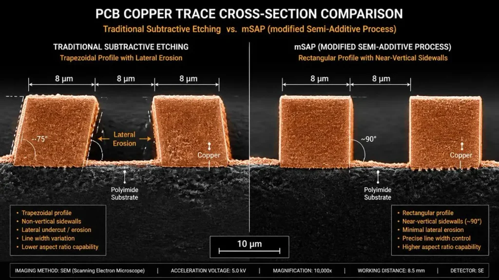
PCB Copper Trace Cross-Section Comparison: Subtractive Etching vs. mSAP
For ultra thin polyimide PCB designs with line/space below 50 µm, subtractive etching becomes unreliable. The etch factor in thin copper (1/3 oz, ~12 µm) creates trapezoidal trace profiles that compromise impedance control and reduce current capacity. Modified Semi-Additive Process (mSAP) is the 2026 standard for fine-line polyimide flexible PCB work: it starts with ultra-thin seed copper (3–5 µm), adds photoresist, plates additional copper only where traces are needed, then strips the resist and flash-etches the seed layer. The result is near-vertical trace sidewalls and line/space down to 8 µm/8 µm in production.
At Hongda Circuit, our mSAP line is not a pilot project. It is a production reality shipping thin polyimide circuit boards to optical transceiver and medical imaging customers with documented impedance coupons and S-parameter reports. If your design calls for 30 µm line/space or finer, ask your supplier for mSAP microsections and yield data. A fabricator without qualified mSAP capability is not a viable partner for advanced ultra thin flexible printed circuit board programs in 2026.
Metrology and Inspection: Verifying Polyimide Flexible PCB Quality Beyond Sample Boards
Every supplier will send you a beautiful sample board. The question is whether they can repeat that quality at 1,000 pieces, 10,000 pieces, and 100,000 pieces. For ultra thin polyimide PCB procurement, the verification stack should include:
- 3D AOI for coverlay registration and trace geometry
- X-ray inspection (Nordson DAGE or equivalent) for microvia void detection
- Cross-section microscopy for via wall copper thickness and nail head evaluation
- TDR impedance testing for controlled thin polyimide circuit differential pairs
- Thermal cycling chambers for reliability validation per IPC-TM-650
Our quality system at PCBkr integrates all of the above, with ISO 9001:2026, AS9100D (aerospace), IATF 16949 (automotive), and IPC-6012 Class 3/3A certification. For medical device OEMs, we maintain ISO 13485 compliance on dedicated production lanes. We provide full lot traceability from raw material certificate through final electrical test—a requirement that commodity flex PCB houses often cannot meet.
Shenzhen Hongda Circuit Technology Co., Ltd. — Production Reality for Ultra-Thin PI PCB Programs
Equipment Portfolio: From LDI Imaging to Femtosecond Laser Platforms
Our Baoan, Shenzhen facility is configured specifically for high-mix, high-reliability polyimide flexible PCB production. The equipment list relevant to ultra thin polyimide PCB programs includes:
- SCREEN Ledia LDI Exposure Machine: Direct imaging for soldermask and etch resist, eliminating phototool degradation that causes pad-size variation in fine-pitch thin polyimide circuit designs.
- Mitsubishi UV/CO₂ Hybrid Laser Drilling: Microvia formation down to 75 µm in PI dielectric, with zero residual stub capability for high-speed ultra thin flex PCB applications.
- LAUFFER Lamination System: Controlled-pressure vacuum lamination that prevents resin squeeze-out and coverlay misregistration in sub-0.20 mm stacks.
- HX Automated Plating Line: Vertical continuous plating (VCP) for uniform via wall copper thickness, critical for multilayer polyimide flexible PCB reliability.
- Nordson DAGE X-Ray Tester: 3D X-ray for void detection in stacked microvias before surface finish application.
- Fischer XRF Spectrometers: Non-destructive gold/nickel thickness measurement with NIST-traceable calibration, programmed for pad-specific readings on ultra thin PI PCB arrays.
This is not a marketing list. It is the actual production floor configuration that builds your thin polyimide circuit boards, and we welcome customer audits to verify it.
Certification Stack: AS9100D, IATF 16949, and IPC-6012 Class 3 for Thin Polyimide Flex Circuits
Certifications are not decorations—they are evidence that a supplier’s process control has been validated by third-party auditors against industry-accepted standards. For ultra thin polyimide PCB programs, the minimum certification profile should include:
- ISO 9001:2026: Foundation quality management system
- IPC-6012 Class 3/3A: High-reliability performance requirements for polyimide flexible PCB
- IATF 16949: Automotive sector quality discipline, including PPAP and control plan methodology
- AS9100D: Aerospace quality management, with full material traceability and FAIR (First Article Inspection Report) documentation
- ISO 13485: Medical device quality system for biocompatible thin polyimide circuit applications
Hongda Circuit maintains all five certifications simultaneously. This means a medical device OEM sourcing a ultra thin flex PCB for a diagnostic patch receives the same lot traceability and process control as an aerospace prime contractor sourcing a rigid-flex satellite interconnect. Procurement teams should verify certification validity through the issuing registrar (e.g., SGS, BV, TÜV), not accept a PDF logo at face value.
Real Production Data: 2.5 Million Microvias Daily and 8μm/8μm Line/Space Capability
Marketing claims dissolve under the weight of production data. Here is what our ultra thin polyimide PCB production line actually delivered in Q3 2026:
- Daily microvia output: 2.5 million vias across UV and femtosecond laser platforms
- Fine-line capability: 8 µm/8 µm line/space in mSAP production for optical interposer customers
- Thickness control: ±5 µm total thickness variation on 0.10 mm thin polyimide circuit panels (measured via in-line micrometer)
- Yield rate: 96.4% first-pass yield on 4-layer polyimide flexible PCB programs with 50 µm microvias
- On-time delivery: 97.2% for prototype and pilot production lots in the 12 months ending August 2026
These numbers are not projections. They are extracted from our ERP and SPC systems, and we provide them in customer quarterly business reviews upon request. When a procurement team evaluates ultra thin PI PCB suppliers, demand equivalent data. A supplier who cannot produce yield and OTD statistics is managing by hope, not by process.
Design for Manufacturing: Ultra-Thin Polyimide PCB DFM Guidelines That Reduce Risk
Bend Radius Specification for Dynamic Folding Applications
The most expensive mistake in ultra thin flex PCB design is specifying a bend radius smaller than the material stackup can survive. The industry rule of thumb—bend radius ≥ 6× total thickness—applies to static flex applications. For dynamic folding, such as the hinge in a foldable phone or the flexing joint in a robotic cable, the safe minimum is 10× to 15× total thickness. A 0.10 mm thin polyimide circuit therefore requires a 1.0–1.5 mm bend radius for dynamic endurance.
At Hongda Circuit, our DFM team uses finite element analysis (FEA) tools to model copper grain strain in the bend zone. We frequently recommend: (1) reducing copper thickness from 1/2 oz to 1/3 oz in the flex region, (2) orienting traces perpendicular to the bend axis to minimize tensile strain, and (3) adding a 0.5 mm keep-out zone around the bend radius where no vias or component pads are placed. These recommendations are provided in our 24-hour DFM report, not as after-the-fact excuses for failure.
Stiffener Design and Coverlay Window Optimization in Thin Polyimide Circuits
Stiffeners on polyimide flexible PCB assemblies serve two purposes: mechanical support for connector insertion, and strain relief at the rigid-to-flex transition. For ultra thin polyimide PCB programs, stiffener material selection is constrained by total thickness budget. FR-4 stiffeners add rigidity but increase thickness by 0.20–1.00 mm. PI stiffeners (50–125 µm) add minimal thickness but provide less mechanical support. Aluminum stiffeners offer thermal conductivity but require insulating adhesive to prevent shorting.
Our standard recommendation for ultra thin flex PCB connector zones is a 0.20 mm PI stiffener laminated with thermosetting adhesive, combined with a stainless steel insertion reinforcement if mechanical durability is critical. The coverlay window—the opening in the PI cover film that exposes solder pads—must extend 0.25 mm beyond the stiffener edge to prevent adhesive squeeze-out from contaminating the pad surface. This level of detail matters when the entire thin polyimide circuit is thinner than a credit card.
Impedance Control Strategies for Ultra-Thin Flex PCB Signal Integrity
High-speed signals on polyimide flexible PCB face unique challenges: the thin dielectric (12.5–50 µm PI) creates tight coupling between signal and reference layers, while the flexibility requirement prevents the use of rigid dielectric prepregs that would stabilize impedance. For ultra thin polyimide PCB designs running USB 3.2, MIPI, or PCIe lanes, we implement:
- Coplanar waveguide with ground (CPWG) routing to maintain consistent impedance without relying on thick dielectric spacing
- Reference plane stitching every 5 mm along the flex route to prevent ground plane discontinuity
- Coverlay thickness control within ±2 µm, because a 25 µm coverlay variation changes single-ended impedance by approximately 3–4 ohms in a 0.10 mm stackup
Our TDR impedance testing validates these structures against customer stackup requirements, with test coupons included in every production lot. For ultra thin flexible printed circuit board programs with 224G PAM4 or equivalent high-speed requirements, we provide S-parameter extraction up to 56 GHz using calibrated VNA measurement.
Application-Specific Guidance: Matching Thin Polyimide Circuit Construction to End Use
Medical Device Integration: Biocompatible Ultra-Thin Polyimide PCB Requirements
Medical ultra thin polyimide PCB applications—diagnostic patches, implantable sensors, catheter interconnects—demand more than electrical performance. The materials must meet biocompatibility standards (ISO 10993 or USP Class VI), and the manufacturing environment must prevent particulate contamination that could trigger immune response. At Hongda Circuit, our ISO 13485 production lanes use dedicated tooling, controlled humidity (<40% RH), and ionized air blow-off before packaging to eliminate foreign material.
For implantable or long-term wear thin polyimide circuit applications, we specify medical-grade PI films with enhanced purity and low outgassing properties. The ENIG surface finish is preferred over OSP for medical polyimide flexible PCB because of its shelf stability and wire-bonding compatibility. Lead times for medical-grade FCCL are typically 3–4 weeks longer than commercial grades, so procurement teams should factor this into program schedules.
Foldable Display and Con
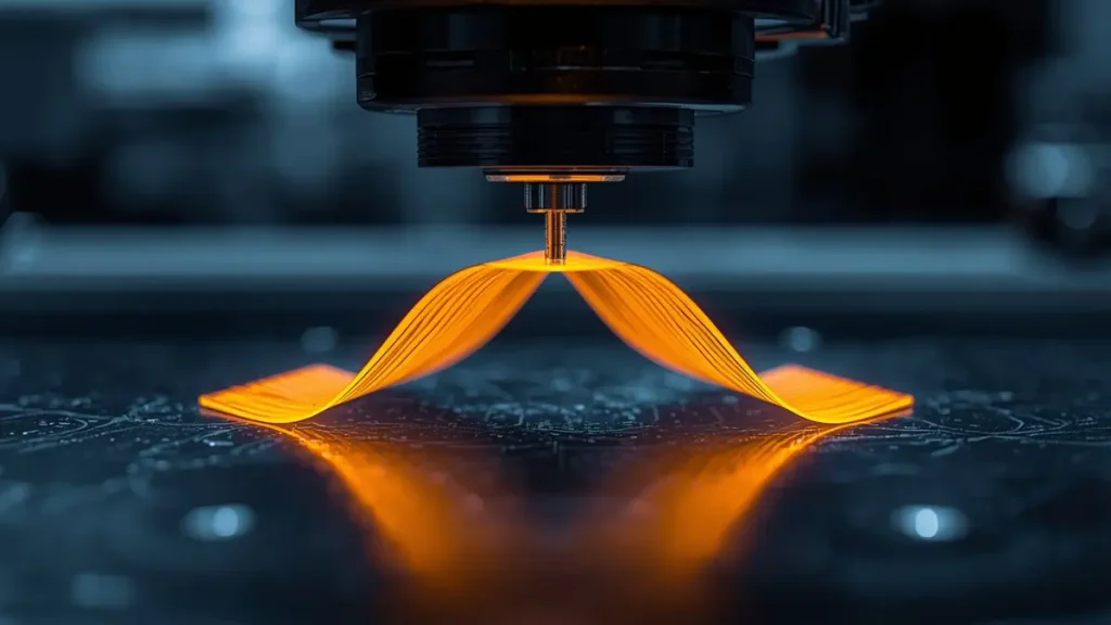
Dynamic Flex Endurance Bending Test for Polyimide FPCsumer Electronics: Dynamic Flex Endurance Standards
The foldable electronics market—smartphones, tablets, laptops—has created the most demanding ultra thin flex PCB reliability requirement in the industry: 200,000+ mechanical fold cycles without electrical failure. Samsung Display’s 2024 qualification of multi-layer flexible PCBs for bend radii below 1.5 mm, verified by TÜV Rheinland, set the benchmark that procurement teams now expect from their supply base.
Achieving this level of dynamic flex endurance in a thin polyimide circuit requires three converging capabilities: (1) RA copper with elongated grain structure oriented along the bend axis, (2) adhesiveless FCCL to eliminate the weakest mechanical layer, and (3) laser-drilled microvias placed outside the bend zone to prevent stress concentration. At PCBkr, we have shipped ultra thin polyimide PCB assemblies for foldable display hinge interconnects since 2024, with documented flex life test data per IPC-6013 Section 3.6. Our standard qualification protocol includes 100,000 cycles at 1.0 mm bend radius as a gate before volume release.
Automotive Sensor Modules: Thermal Cycling Reliability for Polyimide Flexible PCBs
Automotive under-hood and cabin sensor applications expose polyimide flexible PCB assemblies to temperature swings from -40°C to +125°C, with vibration profiles that rigid boards cannot survive. The procurement challenge is balancing the flexibility requirement with the thermal mass and solder joint reliability needed for AEC-Q200 component attachment.
For automotive ultra thin PI PCB programs, we specify high-Tg PI formulations (Tg > 300°C) and ENIG surface finish with 3–5 µin gold thickness to withstand multiple reflow cycles during SMT assembly. Stiffener design is critical: we typically recommend 0.50 mm FR-4 stiffeners at component mounting zones, with a gradual 3 mm transition taper to the flexible section to prevent stress fractures. All automotive thin polyimide circuit lots undergo 1,000-cycle thermal shock testing per IPC-TM-650 Method 2.6.7 before shipment.
Pricing Transparency: Understanding Ultra-Thin Flex PCB Cost Drivers in 2026
Material Selection Impact — Adhesiveless vs. Adhesive-Based PI Lamination
The single largest cost variable in ultra thin polyimide PCB manufacturing is the FCCL construction. Adhesiveless 2L-FCCL costs approximately 30–40% more than adhesive-based 3L-FCCL for equivalent copper weight and PI thickness. The premium reflects the more complex manufacturing process: adhesiveless FCCL requires sputter deposition or plasma-enhanced lamination to bond copper to PI without an intermediate glue layer.
For procurement teams, the decision matrix is straightforward: if the thin polyimide circuit will undergo dynamic bending or must achieve total thickness below 0.15 mm, adhesiveless FCCL is mandatory and the cost premium is non-negotiable. If the application is static flex (installed once and never moved) and total thickness can tolerate 0.20 mm or greater, adhesive-based 3L-FCCL provides acceptable reliability at lower material cost. At Hongda Circuit, we quote both options when the design allows, with a clear explanation of the reliability trade-offs.
Volume Thresholds and Tooling Economics for Low-Volume Thin Polyimide Circuit Orders
Ultra thin flex PCB prototypes (5–20 pieces) carry a disproportionate cost per unit because the tooling—phototools or LDI programming, laser drilling setup, lamination fixtures, and electrical test fixtures—is amortized over a small quantity. For subtractive etch designs, NRE tooling typically ranges from $200–$500. For mSAP polyimide flexible PCB designs with 8 µm/8 µm line/space, the NRE can reach $800–$1,500 due to the specialized photoresist and plating bath preparation.
The volume inflection point for ultra thin polyimide PCB cost competitiveness is typically 500–1,000 pieces, where unit cost drops by 40–60% compared to prototype pricing. For procurement teams managing product development pipelines, we recommend consolidating prototype builds across multiple designs into a single panelization strategy, or committing to a 500-piece pilot run with staged delivery (100 pieces week 1, 400 pieces week 4) to achieve better unit pricing without inflating initial inventory.
FAQ — Procurement Decisions for Ultra-Thin Polyimide PCB Buyers
What is the minimum realistic thickness for an ultra thin polyimide PCB in volume production?
In practical manufacturing terms at Shenzhen Hongda Circuit Technology Co., Ltd., the lower limit for a reliable ultra thin polyimide PCB in volume is 0.05 mm (50 µm) for a single-layer construction with 12.5 µm PI base, 12 µm RA copper, and 12.5 µm PI coverlay. Below this threshold, handling during SMT assembly becomes problematic—panels warp during solder paste printing, and component placement accuracy degrades. For multilayer thin polyimide circuit designs, 0.10 mm is the practical minimum for 2-layer constructions, and 0.20 mm for 4-layer with microvias. We have built 0.03 mm prototypes for R&D programs, but these require specialized carrier jigs for assembly and are not economically viable beyond 100 pieces.
How do I verify that a supplier’s “ultra thin flex PCB” capability is real and not just a marketing claim?
Demand four specific pieces of evidence before placing an order: (1) microsection photographs of their finest line/space in production, with measurement scale, not renderings; (2) a list of installed laser drilling machines with model numbers and installation dates; (3) current certification certificates from accredited registrars (SGS, TÜV, BV), verifiable via the registrar’s online database; and (4) yield data for the last 90 days on polyimide flexible PCB programs with specifications similar to yours. At Hongda Circuit, we provide all four during our qualification phase, and we encourage customer site audits. A supplier who deflects these requests is managing perception, not process.
What is the typical lead time for ultra thin PI PCB prototypes, and what factors extend it?
For qualified designs using stocked materials, our standard ultra thin PI PCB prototype lead time is 5–7 business days. This extends to 10–14 days if: (a) the design requires non-standard PI thickness or copper weight that we must procure from Japan/Korea; (b) the design uses mSAP process and requires photoresist procurement; (c) the design requires medical-grade or aerospace-grade material with lot traceability documentation; or (d) the order includes impedance test coupons and cross-section analysis that add 2–3 days to inspection. We communicate material lead times explicitly in our quotations—no hidden delays after order confirmation.
Should I specify ENIG or OSP surface finish for my thin polyimide circuit application?
For thin polyimide circuit applications, ENIG (Electroless Nickel Immersion Gold) is the default recommendation. ENIG provides a flat, coplanar surface ideal for fine-pitch component placement, offers 12+ month shelf life without oxidation, and is compatible with wire bonding and press-fit connectors. OSP (Organic Solderability Preservative) is lower cost but has a 6-month shelf life and is not suitable for gold wire bonding or multiple reflow cycles. The only scenario where we recommend OSP for ultra thin flex PCB is single-sided, single-reflow consumer electronics with immediate assembly and no connector insertion requirements. For all other applications—medical, automotive, aerospace, high-reliability consumer—ENIG is the risk-adjusted choice.
What DFM information should I provide to my ultra thin polyimide PCB supplier to avoid prototype failure?
Provide five critical data points in your RFQ: (1) the mechanical bend radius and whether the flex is static (installed once) or dynamic (repeatedly flexed); (2) the maximum allowable finished thickness, including stiffeners and coverlay; (3) the component placement and connector insertion force requirements, which determine stiffener material and thickness; (4) the operating temperature range and whether the board will see lead-free reflow; and (5) any impedance control requirements with target values and tolerance. With this information, our engineering team can flag unmanufacturable features before tooling begins, typically saving 1–2 prototype iterations and 3–4 weeks of schedule.
Next Steps — Requesting a DFM Review and Quotation from PCBkr
If your program requires a ultra thin polyimide PCB, thin polyimide circuit, or polyimide flexible PCB with verified manufacturing discipline, submit your Gerber files, stackup requirements, and mechanical drawings to sales@pcbkr.com. Our engineering team will return a complimentary DFM review within 24 hours, including: manufacturability flags, material recommendations, bend radius validation, and a detailed quotation with lead time and lot traceability documentation.
Shenzhen Hongda Circuit Technology Co., Ltd.
- Website: www.pcbkr.com
- Sales Email: sales@pcbkr.com
- Engineering Email: pcb@pcbkr.com
- Phone: +86 0755 23720053
- Address: Room 1608-1610, Research Development Comprehensive Building, Baoyunda Logistics Center, Baoan, Shenzhen, China
- Unified Social Credit Code: 91440300MA5F6CA091
- Certifications: ISO 9001:2026 | AS9100D | IATF 16949 | IPC-6012 Class 3/3A | ISO 13485
This technical guide was prepared by the engineering team at Shenzhen Hongda Circuit Technology Co., Ltd. and reflects production data validated through Q3 2026. For technical clarifications or custom specifications, contact our application engineering division.
About Author
David Chen https://www.linkedin.com/in/pcbcoming
David Chen boasts an extensive professional background in PCBA manufacturing, PCBA testing, and PCBA optimization, with specialized expertise in high-precision PCBA fault analysis and rigorous PCBA reliability testing. The author has worked with high-layer-count server PCB fabrication, ultra-low-loss backplane stackups, and thermo-mechanical reliability optimization for AI infrastructure projects involving 112G and 224G PAM4 architectures. Skilled in complex circuit design and cutting-edge advanced PCB manufacturing processes, he delivers solutions that elevate product durability and performance across industrial applications. His technical articles focusing on PCBA manufacturing workflows and testing methodologies are widely cited by industry peers, research institutions, and technical platforms, solidifying his reputation as a recognized technical authority in the global circuit board manufacturing sector.