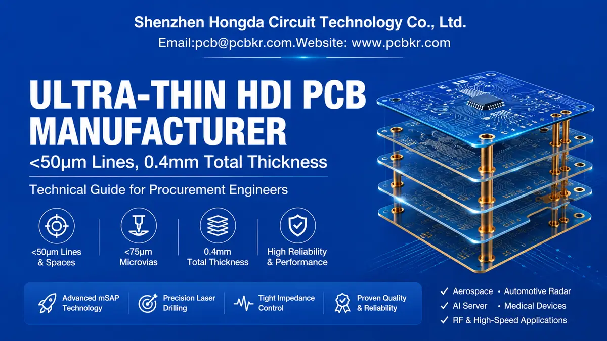
Ultra-Thin HDI PCB Manufacturer: <50μm Lines, 0.4mm Total Thickness | Hongda Circuit
Shenzhen Hongda Circuit Technology Co., Ltd. manufactures ultra-thin HDI PCB substrates for hardware teams that cannot afford field failures. If you are sourcing thin HDI PCB stacks for aerospace avionics, 77GHz automotive radar, or AI server OAM modules, the gap between a supplier’s marketing slide and their actual lamination press is where projects die.
Most procurement teams evaluating ultra-thin high density PCB vendors hit the same wall: capability claims without data, quotes that balloon after NPI, and microvia failures that surface six months into deployment. This guide eliminates that ambiguity. It maps the technical thresholds that separate real ultra-thin HDI factories from standard HDI shops posing as advanced manufacturers, and it gives you a verifiable RFQ checklist to audit any supplier—including us.
What Is Ultra-Thin HDI PCB? Technical Thresholds vs. Standard HDI
Defining the Ultra-Thin HDI PCB Category
An ultra thin HDI PCB is not simply a thin board with small vias. It is a multilayer substrate that simultaneously satisfies two independent constraints:
- Total board thickness ≤ 0.8 mm, with specialized applications pushing below 0.4 mm.
- Interconnect density requiring microvias and fine-line lithography—specifically line/space below 50 μm and microvia diameters below 75 μm.
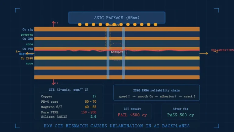
Standard HDI fabricators routinely produce 50/50 μm line/space on 1.0 mm+ cores. That is conventional HDI. When your stackup compresses dielectric layers to 15–35 μm using ABF film or ultra-thin prepreg, and your core drops to 0.10–0.20 mm, you have crossed into ultra-thin high density PCB territory. The manufacturing physics change: subtractive etching becomes impossible, lamination registration tolerance tightens from ±25 μm to ±10 μm, and thermal expansion mismatches between ultra-thin copper and low-modulus dielectrics cause delamination if the oxide-alternative bonding chemistry is not precisely controlled.
Ultra-Thin HDI vs. Standard HDI—Capability Matrix
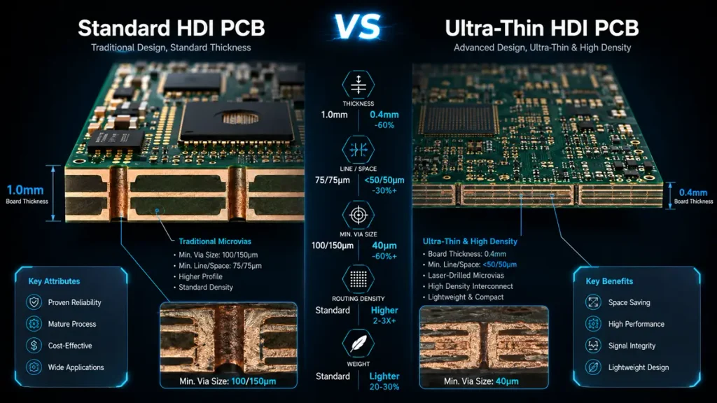
Standard HDI vs Ultra-Thin HDI PCB Capability Comparison
Use this table to audit a supplier’s actual equipment. If they cannot quote process data in these ranges, they are not building ultra-thin HDI.
| Feature | Standard HDI | Ultra-Thin HDI (This Page Scope) |
| Line/Space | 50–100 μm | < 50 μm (25 μm qualified) |
| Microvia Diameter | 75–125 μm | < 75 μm (down to 40–50 μm) |
| Dielectric Thickness | 50–100 μm | 15–35 μm (ABF film) |
| Core Thickness | 0.20–1.6 mm | 0.10–0.20 mm |
| Total Board Thickness | ≥ 1.0 mm | ≤ 0.8 mm (specialty ≤ 0.4 mm) |
| Primary Process | Subtractive etching | mSAP / SAP semi-additive |
| Impedance Tolerance | ±10% | ±5% with TDR validation |
At Hongda Circuit, our mass-production standard for thin HDI PCB builds holds 45/45 μm line/space on 0.4 mm total thickness, with sample qualification down to 25/25 μm using mSAP. Our laser drilling alignment is maintained within ±10 μm—tight enough to land 50 μm microvias on 0.35 mm pitch BGA pads without breakout.
Stackup Design for Ultra-Thin HDI: 1+4+1, 2+4+2, Any-Layer Options
Recommended Buildups for Sub-0.8mm Stacks
Not every layer configuration survives sequential lamination at sub-millimeter thickness. For ultra-thin HDI PCB procurement, we restrict stackup recommendations to proven configurations that balance routing density against mechanical rigidity:
- 1+4+1 (6-layer): Baseline for industrial vision modules and medical endoscopes. Total thickness 0.4–0.6 mm. One lamination cycle. Cost-optimized for medium-density BGA fanout.
- 2+4+2 (8-layer): Standard for automotive radar and compact RF front-ends. Two lamination cycles. Supports staggered microvias with 30 μm dielectric between build-up layers.
- Any-Layer ELIC (10–16 layer): Required for AI server OAM modules and smartphone camera substrates. Every layer pair interconnects via stacked copper-filled microvias. Total thickness can be held at 0.4 mm with 0.10 mm ultra-thin cores.
The mistake we see in incoming RFQs is specifying Any-Layer HDI when 1+N+1 would suffice. Any-Layer adds 35–40% processing cost due to repeated laser drilling and lamination cycles. Our DFM team reviews every stackup before quoting. If we can solve your routing problem with a 2+N+2 thin HDI PCB instead of ELIC, we will tell you in the first 12 hours.
Critical Stackup Parameters Buyers Must Specify
When you send an RFQ for an ultra-thin high density PCB, include these five parameters or expect a 40% quote variance between suppliers:
- Dielectric material and thickness per ply. Specify ABF GL102 (15 μm) vs. high-Tg prepreg (60 μm). This determines laser drilling energy and impedance.
- Copper weight by layer. Signal layers at 0.5 oz (18 μm) enable fine-line etching; power layers at 1 oz carry current but limit trace density.
- Stack symmetry tolerance. We enforce ±8% symmetry to prevent reflow warpage on sub-0.6 mm boards.
- Impedance targets with TDR verification. 50 Ω single-ended and 90–100 Ω differential are standard. Demand ±5% tolerance backed by coupon testing, not calculation-only.
- Microvia aspect ratio. For 50 μm laser-drilled holes in 35 μm dielectric, the aspect ratio is 0.71:1—safe. Push that same hole through 75 μm dielectric and the ratio hits 1.5:1, where plating voids become likely.
Materials & Processes: ABF, mSAP, Laser Drilling, Impedance Control
Why mSAP Replaces Subtractive Etching Below 30 μm
Subtractive etching starts with 18–35 μm copper foil and removes unwanted metal. At line/space below 50 μm, isotropic undercut becomes uncontrollable. A 5 μm width variation shifts characteristic impedance by 2–3 Ω—unacceptable for 112G PAM4 channels.
Our mSAP (Modified Semi-Additive Process) line at Hongda Circuit operates as follows:
- Laminate 1.5–3 μm ultra-thin copper seed layer onto the dielectric.
- Image the trace pattern using SCREEN Ledia LDI exposure at ±1.5 μm accuracy.
- Selectively plate copper to target height (15–20 μm).
- Flash-etch the seed layer.
The result is near-vertical trace sidewalls with minimal undercut. We hold 20/20 μm in volume production and have qualified 8/8 μm for substrate-like PCB (SLP) builds. If your supplier still quotes subtractive etching for 30 μm lines, they are not manufacturing ultra-thin HDI PCB stacks—they are gambling with your yield.
Laser Drilling and Via Architecture
Our Mitsubishi UV/CO₂ hybrid laser systems drill microvias down to 50 μm in mass production, with positioning accuracy within ±10 μm. For R&D samples, we have qualified 20 μm blind vias using femtosecond laser sources.
The via architecture matters as much as the hole size:
- Staggered microvias: Lower cost, higher reliability. Each via lands on solid copper. We recommend these for automotive and medical applications where thermal cycling exceeds 1,000 cycles.
- Stacked microvias: Required for Any-Layer ELIC and 0.35 mm pitch BGA escape routing. These demand copper-filled vias with <5% voids per IPC-4761 Type VII. Our pulse electroplating line achieves this with uniform hole-wall copper thickness controlled within ±2 μm.
Material Stack for Signal Integrity at 224G PAM4
Ultra-thin HDI PCB material selection in 2026 has shifted. Standard FR-4 does not survive the Dk/Df requirements of AI server and 6G hardware. Our approved material list includes:
- M9-grade ultra-low-loss CCL: Dk ≤ 3.0, Df ≤ 0.0008 @ 10 GHz. Composed of hydrocarbon/modified PPO resin, high-purity quartz cloth (Q-cloth), and HVLP5 ultra-low-profile copper foil. This is the baseline for 224G PAM4 backplanes.
- Megtron 6/7: For 112G applications where cost optimization matters.
- ABF (Ajinomoto GL102 / GZ41): 15–35 μm build-up dielectric for ultra-thin coreless substrates.
Surface finishes for flip-chip and wire-bond compatibility include ENEPIG, EPIG, and hard gold down to 150 μm pitch.
Digital Twin Process Monitoring
In 2026, leading ultra-thin high density PCB suppliers operate digital twin environments where each panel’s process parameters—etch chemistry, laser energy, plating current density, lamination press profiles—are logged per job. At Hongda Circuit, this traceability data is exportable as a structured report alongside your shipped boards. If your application requires AS9100D or ISO 13485 compliance, this level of lot traceability is not optional—it is a procurement qualifier.
Applications: Aerospace, Automotive Radar, AI Server Modules
Every application below demands both “ultra-thin” and “high-density” simultaneously. A standard HDI supplier cannot substitute.
Aerospace Avionics and Satellite Payloads
Space-constrained avionics boxes and CubeSat payloads require total thickness ≤ 0.6 mm with high reliability. Our ultra-thin HDI PCB stacks for aerospace use high-Tg BT resin cores, symmetric build-ups to prevent outgassing-induced delamination in vacuum, and full IPC Class 3 inspection with 100% 3D X-Ray.
Automotive 77GHz Radar and ADAS Camera Modules
Millimeter-wave radar PCBs cannot tolerate impedance discontinuities. A 50 μm microvia with poor plating creates a reflection point that degrades 77GHz signal integrity. Our thin HDI PCB builds for automotive radar use staggered microvias, low-Dk dielectrics, and IATF 16949-controlled processes with PPAP documentation available on request.
AI Server OAM and GPU Modules
AI accelerators route 112G–224G PAM4 signals through 0.4 mm pitch BGA fields. The only practical escape is Any-Layer HDI with stacked microvias and via-in-pad (VIPPO) design. We ship 6+N+6 and 7+N+7 builds with M9-grade materials, impedance coupons, and TDR reports verifying insertion loss budgets.
How to Specify Your Ultra-Thin HDI: RFQ Checklist for Procurement Teams
This section addresses the most common pain point in thin HDI PCB sourcing: comparing quotes that describe entirely different products. Two suppliers can quote the same Gerber set with a 60% price spread and both be “correct”—because they assumed different materials, impedance verification methods, and IPC classes.
The 8-Point Ultra-Thin HDI PCB RFQ Checklist
Before you send a request for quotation, require every vendor to complete this template. A supplier that refuses is, by definition, not controlling those variables.
| Checklist Item | Why It Matters | Hongda Circuit Standard |
| 1. Laminate material (mfg + part number) | M9-grade vs. standard FR-4 changes Dk by 30% and cost by 25%. | Panasonic Megtron 7/8, Isola Tachyon 100G, M9-grade CCL |
| 2. Surface finish spec | ENEPIG vs. ENIG impacts wire-bond reliability and shelf life. | ENEPIG per IPC-4556, EPIG, hard gold |
| 3. Solder mask brand/color | Generic mask cracks on ultra-thin cores during reflow. | Taiyo PSR-4000 series or equivalent |
| 4. Impedance tolerance + verification | Calculation-only is not validation. Demand TDR coupons. | ±5% with TDR coupon report per IPC-2141A |
| 5. IPC Class (2 or 3) | Class 3 requires microsection inspection; Class 2 does not. | IPC-A-600 Class 3 standard; Class 3A available |
| 6. Panel size and array configuration | Determines yield and tooling cost. | Optimized for your SMT line requirements |
| 7. Electrical test method | Flying probe misses microvia continuity at volume. | Flying probe for prototypes; grid test for mass production |
| 8. Delivery terms (EXW vs. DDP) | Customs delays can add 2 weeks to “5-day sample” promises. | EXW, FOB, DDP available with full documentation |
Supplier Capability Audit: 5 Questions That Expose Weaknesses
Send these questions before you issue a PO. The answers separate actual ultra-thin HDI PCB manufacturers from brokers and standard-fab shops.
- “Show me a microsection of a 25/25 μm mSAP trace on ABF.” If they cannot produce a cross-section photo with measurement data, they do not run mSAP.
- “What is your laser drilling positional accuracy, and how often is it calibrated?” We answer: ±10 μm, calibrated weekly against NIST-traceable standards.
- “Provide a TDR report for a 100 Ω differential pair on 0.4 mm total thickness.” This verifies they have built and tested the exact stackup you need, not just simulated it.
- “What is your mass-production yield for 6+N+6 Any-Layer HDI?” Our AI-driven inspection system holds >96% first-pass yield on 10–16 layer camera HDI modules.
- “Can I have real-time production tracking?” Our AI-driven ERP provides job-level status updates, not just “in production” email replies.
Why Choose Hongda Circuit? SAP Capability, TDR Reports, 5-Day Samples
Verified Equipment, Not Marketing Claims
Our 12,000 m² facility in Bao’an, Shenzhen runs the following equipment list—available for virtual or on-site audit:
- Mitsubishi UV/CO₂ hybrid laser drills for 50 μm microvias with ±10 μm registration.
- SCREEN Ledia LDI exposure for 25 μm line/space imaging.
- LAUFFER vacuum lamination presses for thin-core symmetric stack bonding.
- Pulse electroplating lines for void-free copper fill in stacked microvias.
- Nordson DAGE 3D X-Ray and AI-enhanced AOI for 100% microvia inspection.
- TDR impedance test stations with ±5% validation on every impedance-controlled order.
Certifications That Matter for B2B Procurement
- ISO 9001 (Quality Management)
- IATF 16949 (Automotive)
- ISO 13485 (Medical Devices)
- AS9100D (Aerospace)
- IPC-A-600 Class 3
- UL Recognition
Procurement-Friendly Service Model
- 30-minute inquiry response. No web forms—email sales@pcbkr.com directly.
- 12-hour DFM review. Our engineers identify stackup risks before you cut a panel.
- 5-day ultra-thin HDI PCB prototype turnaround for qualified 1+N+1 and 2+N+2 builds.
- No MOQ. We prototype 5 pieces and scale to 100,000+ without changing your process flow.
- Full lot traceability. Every panel links back to laser drilling parameters, plating bath chemistry, and AOI images.
Frequently Asked Questions: Ultra-Thin HDI PCB Sourcing from a Buyer’s Perspective
How do I verify that a supplier can actually manufacture ultra-thin HDI PCB with 25 μm lines, not just quote it?
Demand three documents before issuing a PO: (1) a microsection photograph of a 25/25 μm mSAP trace with measured width data; (2) a TDR impedance report for a sub-0.8 mm board in your target material system; (3) a process flow diagram showing mSAP, laser drilling, and sequential lamination steps. At Hongda Circuit, we provide all three during the qualification phase. A supplier that hesitates is either subcontracting or running subtractive etching and hoping for tolerance luck.
Why do quotes for the same thin HDI PCB Gerber vary by 40–60% between China suppliers?
Because “HDI” is not a standardized term. One vendor quotes subtractive etching on standard FR-4 with 75 μm microvias. Another quotes mSAP on M9-grade material with 50 μm stacked vias, TDR validation, and IPC Class 3 inspection. Those are different products. Use the 8-point RFQ checklist above to force apples-to-apples comparisons. We itemize every process step, material SKU, and test method in our quotes so you see exactly what drives the cost.
What is the real lead time for ultra-thin HDI PCB prototypes, and what causes delays?
A qualified 1+N+1 or 2+N+2 thin HDI PCB prototype ships in 5–7 days if the stackup uses standard materials and the design passes DFM without revision. Delays come from three sources: (1) material allocation—M9-grade laminates currently carry 16–20 week lead times in the open market, but we stock Megtron 7/8 and M9 substrates for qualified customers; (2) DFM revisions requested after CAM review; (3) impedance re-spins caused by stackup miscalculations. We eliminate source #2 by providing free DFM within 12 hours of Gerber receipt.
My last supplier had microvia failures after 500 thermal cycles. What process controls prevent this in ultra-thin high density PCB builds?
Microvia failure in thermal cycling stems from plating voids or excessive aspect ratio. Our controls: (1) Pulse electroplating with uniform hole-wall copper thickness within ±2 μm, verified by microsection; (2) Aspect ratio cap at 0.75:1 for blind vias in ultra-thin dielectrics; (3) 100% 3D X-Ray inspection for void detection before lamination; (4) Post-plating thermal stress test per IPC-TM-650 2.6.8 on every production lot. For automotive and aerospace programs, we add -40°C to +125°C thermal shock profiling with full batch documentation.
Can Hongda Circuit support both ultra-thin HDI PCB prototype NPI and volume production without changing the process flow?
Yes. We maintain separate fast-turn NPI lines and high-volume production lines. The NPI line uses the same mSAP, LDI, and laser drilling equipment as mass production—there is no process translation risk when you scale from 10 pieces to 10,000 pieces. Our AI-driven ERP tracks every panel by serial number, so the laser energy, plating current, and lamination pressure that qualified your prototype are locked in for the production batch.
Ready to move from supplier evaluation to qualified samples?
Email your stackup requirements and Gerber files to sales@pcbkr.com. Our engineering team will return a detailed DFM assessment, cross-section qualification data, and a fixed-price quote within 30 minutes.
Shenzhen Hongda Circuit Technology Co., Ltd. Room 1608-1610, R&D Comprehensive Building, Baoyunda Logistics Center, Bao’an District, Shenzhen, China Website: www.pcbkr.com Email: sales@pcbkr.com | pcb@pcbkr.com Tel: +86 0755 23720053
About Author
David Chen https://www.linkedin.com/in/pcbcoming
David Chen boasts an extensive professional background in PCBA manufacturing, PCBA testing, and PCBA optimization, with specialized expertise in high-precision PCBA fault analysis and rigorous PCBA reliability testing. The author has worked with high-layer-count server PCB fabrication, ultra-low-loss backplane stackups, and thermo-mechanical reliability optimization for AI infrastructure projects involving 112G and 224G PAM4 architectures. Skilled in complex circuit design and cutting-edge advanced PCB manufacturing processes, he delivers solutions that elevate product durability and performance across industrial applications. His technical articles focusing on PCBA manufacturing workflows and testing methodologies are widely cited by industry peers, research institutions, and technical platforms, solidifying his reputation as a recognized technical authority in the global circuit board manufacturing sector.