
Ultra-Thin PCB Procurement Guide: Where to Buy, How Much It Costs, and How to Verify Your Supplier Can Build It
How to Source Ultra-Thin PCBs? If you are a procurement manager, hardware engineer, or OEM sourcing lead tasked with purchasing ultra-thin printed circuit boards, you have probably already hit the same wall that stalls most buying cycles. On the surface, suppliers claim full production capability, and the quoted price seems reasonable. However, problems always arise three weeks into the project: 0.2 mm boards warp beyond IPC limits, microvias are drilled off-center, and trace geometry collapses during subtractive etching. These issues cause project delays, result in scrapped tooling, and leave you answering for why such risks were not identified in the early RFQ stage.
This guide is not another generic explanation of ultra-thin PCB basics. It is a professional procurement decision framework focusing exclusively on 0.1–0.4 mm thick PCBs, built around six core questions that effectively guide supplier selection, cost control and risk mitigation. Every section contains actionable checklists, industry price benchmarks, and specific equipment and process verification criteria that you must confirm before issuing a purchase order.
1.Where Can I Buy Ultra-Thin PCB? Evaluating Supplier Types and Sourcing Channels
The first decision in any ultra-thin PCB procurement cycle is not “Who is cheapest?” It is “Who actually owns the process?” The answer determines whether you are dealing with a fabricator that controls lamination pressure, laser registration, and mSAP chemistry—or a broker who forwards your Gerbers to an anonymous third floor in Shenzhen and hopes for the best.
1.1. PCB Specialized Factory vs. Turnkey PCBA vs. Trading Platform: Which Channel Fits Your Project?
PCB Specialized Factory (Direct Manufacturer)
This is the only channel we recommend for ultra-thin builds below 0.3 mm. A dedicated PCB factory owns the critical process chain: vacuum lamination, LDI imaging, laser drilling, and mSAP plating. At Shenzhen Hongda Circuit Technology, our Baoan facility runs every one of these steps in-house. We do not outsource thin-core lamination or mSAP seed-layer deposition to subcontractors because the registration tolerance between those steps is tighter than what a dispersed supply chain can hold.
Turnkey PCBA Factory (PCB + Assembly + Test)
Turnkey providers are convenient when your project needs SMT, ICT, and functional test under one roof. The risk is that many PCBA houses subcontract the bare-board fabrication to a lower-tier shop that treats ultra-thin panels like standard 1.6 mm boards. If you choose this route, demand the bare-board fabricator’s name, their IPC-6012 Class rating, and proof of in-house mSAP capability. Do not accept “We have a partner for that” as an answer for boards under 0.25 mm.
Trading Platform / Broker (Alibaba, Made-in-China, Global Sources)
Platforms are useful for initial supplier discovery, but they are dangerous as a sole sourcing channel for ultra-thin PCBs. The typical broker model adds 15–30% margin, obscures the real factory identity, and inserts a communication layer that garbles stack-up requirements. We have seen RFQs where a broker translated “0.15 mm ±0.05 mm” into “0.15 mm nominal”—a difference that turned a valid specification into a rejected lot. Use platforms for market scanning; qualify the factory directly before committing tooling.
1.2. Five Critical Dimensions for Selecting an Ultra-Thin PCB Manufacturer
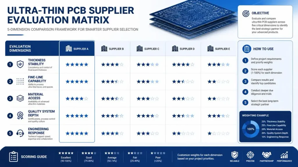
Five Critical Dimensions for Evaluating Ultra-Thin PCB Manufacturers
Use this scorecard when vetting any supplier, including Hongda Circuit:
| Dimension | What to Verify | Red Flag |
| Thickness Stability | Can they hold ±0.05 mm on 0.15–0.20 mm builds across a full panel? | No vacuum-carrier handling; no post-lamination flatness measurement |
| Fine-Line Capability | Do they own LDI and mSAP in-house, or rely on film-based exposure? | Subtractive etching only; no mSAP line |
| Material Access | Do they stock M9-grade CCL, Megtron 7/8, LCP, and thinned FR-4 cores? | Every material is “special order” with 4-week lead time |
| Quality System Depth | ISO 9001 is table stakes. Do they hold IATF 16949, AS9100D, or ISO 13485? | Only ISO 9001; no IPC-6012 Class 3 qualification data |
| Engineering Response | Will a process engineer review your Gerbers and stack-up within 24 hours? | Sales-only contact; no DFM feedback before tooling |
At Hongda Circuit, we publish our capability matrix openly: 0.10 mm minimum for single-layer rigid, 0.15 mm for double-layer, 0.35 mm for 4-layer, and 0.08 mm for flexible circuits. Our mSAP line has qualified 8 μm/8 μm line/space for substrate-like PCB (SLP) builds, and standard ultra-thin production holds 20 μm/20 μm. These numbers are not aspirational; they are what our SCREEN Ledia LDI and Mitsubishi UV/CO₂ laser drilling systems produce daily.
1.3. The RFQ-to-Production Pathway Every Buyer Should Map
A disciplined procurement process for ultra-thin PCBs follows six gates. Skip any of them, and you increase the probability of a mid-project engineering change or a lot rejection at incoming inspection.
- Specification Lock: Gerber/ODB++ + stack-up drawing + impedance table + material callout
- Supplier Capability Audit: Request process capability data (Cp/Cpk) for thickness, trace width, and registration
- DFM Review: The supplier’s engineer flags copper imbalance, via aspect ratio risks, or surface finish incompatibility
- Quotation & Terms: Firm price, locked lead time, Incoterm, and payment structure
- First Article Inspection (FAI): Dimensional, electrical, and cross-sectional validation before volume release
- Volume Ramp: Process qualification (PPAP or equivalent) and statistical process control (SPC) handoff
2. How Much Does Ultra-Thin PCB Cost? Price Benchmarks and Cost Drivers
Price is not the primary cost driver in ultra-thin PCB procurement. Yield loss, redesign loops, and delayed market entry are. That said, you need a realistic budget to secure internal approval and to spot quotes that are either unsustainably low (a warning sign) or inflated by unnecessary process steps.
2.1. Price Ranges by Layer Count and Volume
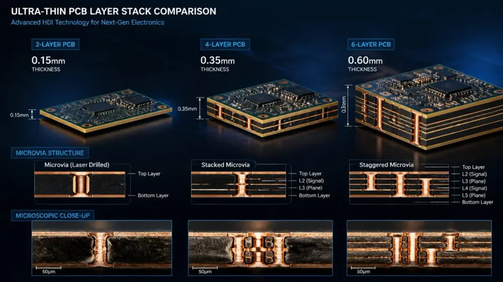
Ultra-Thin PCB Layer Stack Comparison: 2L, 4L, and 6L HDI Architectures
The following figures are based on market data for bare-board fabrication, ENIG finish, standard FR-4 or high-Tg material, and typical panel sizes (≤300 × 400 mm). They assume the supplier holds legitimate mSAP and LDI capability.
| Build Type | Prototype (5–10 pcs) | Small Batch (100–500 pcs) | Volume (1,000+ pcs) | Typical Lead Time |
| 2-Layer Ultra-Thin (0.15–0.20 mm) | $40–$150 | $15–$40 / unit | $8–$25 / unit | 5–8 days proto; 2–3 weeks volume |
| 4-Layer Ultra-Thin (0.35 mm) | $80–$300 | $35–$90 / unit | $18–$55 / unit | 7–10 days proto; 3–4 weeks volume |
| 6-Layer Ultra-Thin (0.60 mm) | $150–$600 | $70–$180 / unit | $35–$110 / unit | 10–14 days proto; 4–5 weeks volume |
| Ultra-Thin HDI (4–8L, microvias) | $300–$1,000+ | $120–$350 / unit | $60–$200 / unit | 12–18 days proto; 5–6 weeks volume |
| Ultra-Thin RF / High-Frequency | $250–$1,000+ | $100–$300 / unit | $50–$180 / unit | 10–15 days proto; 4–5 weeks volume |
The premium over a standard 1.6 mm board is typically 30–50% for 2–4 layer ultra-thin builds, and 60–100% for HDI or fine-line designs. Below 0.20 mm, the premium escalates because panel handling shifts to vacuum carriers, drilling stack heights drop to 2–3 panels, and mSAP replaces subtractive etching.
2.2. Eight Factors That Move the Needle on Ultra-Thin PCB Pricing
- Board Thickness: Below 0.20 mm, handling complexity rises exponentially. A 0.10 mm single-layer board is not simply “half the material” of a 0.20 mm board; it requires carrier fixtures, reduced conveyor speed, and manual inspection at multiple stages.
- Layer Count: Each additional lamination cycle introduces registration risk. A 6-layer board requires two or three lamination presses, and each press must hold ±0.05 mm flatness on a substrate that wants to curl.
- Line Width / Space: Below 50 μm, subtractive etching becomes uncontrollable due to undercut. You need mSAP, which adds seed-layer lamination, selective plating, and flash-etch steps. Below 30 μm, you enter SLP territory where even mSAP equipment must be qualified to sub-micron alignment.
- Material Grade: Standard FR-4 TG130 is the baseline. High-Tg (TG170–180), halogen-free, or M9-grade low-loss laminates can multiply material cost by 3–5×. For AI edge modules or 5G mmWave antennas, this is non-negotiable, but for a simple SIM card carrier, it is over-engineering.
- Surface Finish: ENEPIG costs more than ENIG, which costs more than OSP. For ultra-thin boards, ENIG (2–4 μin gold) is the most common choice because it provides a flat, solderable surface for fine-pitch BGAs without adding significant thickness. At Hongda Circuit, we also offer thin-ENIG (1.5–2.0 μin) for high-frequency applications where every micron of dielectric separation matters.
- Microvia Density: Stacked microvias require sequential lamination and filled-via plating. Each additional lamination cycle adds cost and lead time. A 4-layer board with one lamination cycle and standard through-holes is far cheaper than the same layer count with blind/buried microvias.
- Testing Coverage: 100% AOI + flying probe + X-ray inspection adds 10–20% to the unit price but prevents field failures that cost 100× more. For medical or automotive ultra-thin PCBs, this is not optional.
- Volume and Panel Utilization: Prototype lots (5–10 pcs) carry high non-recurring engineering (NRE) charges because tooling, DFM, and first-article inspection are amortized over a tiny quantity. At 1,000+ panels, the NRE is diluted, and the supplier can optimize panelization to reduce scrap.
2.3. Hidden Costs and Margin-Eaters Most RFQs Miss
- NRE / Tooling Fees: Engineering review, phototool generation (if not LDI), test fixture build, and special carrier design. For ultra-thin boards, expect $200–$800 in NRE for prototypes.
- Low-Yield Surcharges: If your design pushes the supplier’s process window, they may quote a “minimum acceptable yield” clause. Read the fine print. A 70% yield means you pay for 100% of the panels but only receive 70%.
- Expedite Fees: A 5-day prototype lane can become a 3-day lane for a 50–100% surcharge. Define your real deadline before accepting an expedite quote.
- Packaging and Logistics: Ultra-thin boards ship in rigid support frames or vacuum-sealed trays. Air freight from Shenzhen to the US West Coast adds $4–$8 per kg. DDP terms shift customs clearance cost to the supplier but raise the unit price.
- Payment Terms Impact: Net-30 or net-60 terms usually carry a 2–5% price premium versus 100% pre-payment or a 30/70 split. Factor this into your total cost of ownership.
3. Can You Manufacture My Specification? The RFQ Checklist and Capability Verification
This is the question that separates procurement professionals from order-takers. A well-structured RFQ does not just ask for a price; it forces the supplier to prove they understand your stack-up, your tolerance chain, and your reliability requirements.
3.1. The Non-Negotiable Specification Sheet Every Buyer Must Submit
Before you send a single RFQ, lock these parameters internally. Changing them after the supplier starts tooling is the fastest way to burn budget and delay your program.
- Target Thickness and Tolerance: e.g., 0.20 mm ±10% (0.18–0.22 mm). Do not write “0.20 mm nominal.” That is not a tolerance; it is a wish.
- Layer Count and Stack-Up: Core thickness, prepreg type and thickness, copper weight per layer. If you do not know, ask the supplier’s engineer to propose one—but demand they justify it against your impedance requirements.
- Minimum Trace / Space: e.g., 3 mil / 3 mil (75 μm). If you need 2 mil / 2 mil, state it explicitly. This single parameter determines whether the job runs on standard subtractive etching or requires mSAP.
- Minimum Hole Size and Type: Mechanical through-hole vs. laser-drilled microvia. Specify aspect ratio limits (e.g., 10:1 max for mechanical, 0.8:1 for laser).
- Material Specification: FR-4 TG130/170/180, polyimide (PI), liquid crystal polymer (LCP), or M9-grade CCL. If you are unsure, describe the operating environment (temperature, frequency, bend cycles) and let the supplier recommend.
- Surface Finish: ENIG, OSP, ENEPIG, immersion tin, or hard gold. Note any wire-bonding or high-frequency requirements.
- Impedance Control: Single-ended and differential targets, tolerance (typically ±5% or ±10%), and reference layers.
- Outline and Panelization: Board dimensions, panel size, breakaway tab or V-score preference, and any internal cutouts or slots.
- Quality and Test Requirements: IPC-6012 Class 2 or 3, 100% electrical test, AOI, X-ray, cross-section analysis, or reliability testing (thermal shock, bend test).
- Quantity, Delivery, and Incoterm: Prototype count, pilot-run count, mass-production forecast, required delivery date, and shipping terms (EXW, FOB, DDP).
3.2. The Complete RFQ Field List (Ready-to-Use Table)
| Field | Your Input | Why It Matters |
| Gerber / ODB++ / IPC-2581 | File version and date | Ensures the supplier is quoting the correct revision |
| Stack-Up Table | Core and prepreg thicknesses, copper weights | Determines lamination cycles and registration risk |
| Drill Chart | Hole sizes, quantities, plating requirements | Drives drilling time and aspect ratio feasibility |
| Impedance Table | Target Zo, tolerance, trace width | Determines whether mSAP or standard etching is needed |
| Surface Finish | ENIG, OSP, ENEPIG, etc. | Affects cost, shelf life, and assembly compatibility |
| Silkscreen & Soldermask | Color, thickness, brand preference | Some colors (e.g., matte black) require special processing |
| Quality Standard | IPC-6012 Class 2/3, AS9100, IATF 16949 | Determines inspection rigor and acceptance criteria |
| Test Requirements | Flying probe, fixture test, X-ray, cross-section | Adds cost but catches defects before assembly |
| Quantity Breaks | 5, 50, 500, 5,000 pcs | Enables the supplier to optimize panelization and pricing |
| Delivery & Shipping | Date, destination, Incoterm | Affects lead time commitment and freight cost allocation |
3.3. How to Audit a Supplier’s Real Capability—Beyond the Brochure
A glossy capability sheet means nothing if the equipment is offline or the operator was trained last week. Here is how to separate real capability from marketing:
Request Process Capability Data (Cp/Cpk)
Ask for Cpk values on the specific parameters that matter to your design: thickness uniformity, trace width control, layer-to-layer registration, and hole positional accuracy. A Cpk ≥ 1.33 indicates the process is statistically capable. At Hongda Circuit, our mSAP line maintains Cpk > 1.5 on trace width and Cpk > 1.67 on layer registration.
Ask for Similar Project References
Do not accept “We have made thin boards before.” Ask: “Have you produced 0.20 mm 4-layer boards with 3 mil/3 mil traces and laser microvias for a medical device OEM in the last 12 months?” Then request a redacted sample report or FAI data.
Demand Measured Sample Data
Before placing a volume order, request a sample or reference board with full dimensional data: thickness measured at 9 points, trace width on coupon, impedance sweep, and cross-section photomicrographs. At Hongda Circuit, we provide this data as standard on every FAI lot.
Evaluate Engineering Support Depth
Send a deliberately challenging stack-up and see how the supplier responds. Do they flag the copper imbalance? Do they suggest dummy fill or thieving patterns? Do they propose an alternative material that saves cost without sacrificing reliability? A supplier who only quotes what you asked for is a vendor. A supplier who improves your design before tooling is a partner.
4. Lead Time & Order Process: From First Quote to Mass Production
Ultra-thin PCBs do not tolerate rush jobs that skip DFM. The fastest way to miss a market window is to compress the prototype phase so aggressively that the first article fails and you restart at week zero.
4.1. Realistic Lead Time Ranges
| Phase | Standard Lead Time | Expedited Lane | Notes |
| Prototype (2–4L, 5–50 pcs) | 5–8 working days | 3–5 days | Requires locked Gerbers; no spec changes allowed |
| Prototype (6–8L or HDI) | 10–14 working days | 7–10 days | Sequential lamination cannot be compressed below physical cure times |
| Small Batch (100–500 pcs) | 8–12 working days | 5–7 days | Panelization and material prep are the bottlenecks |
| Volume (1,000+ pcs) | 2–3 weeks (standard) | 10–14 days | Depends on material inventory and current fab loading |
| Volume (Any-Layer HDI, M9 material) | 4–5 weeks | 3 weeks | M9-grade CCL may require special-order lead time from Panasonic/Isola |
At Hongda Circuit, our AI-driven ERP system tracks every job in real time, and our on-time delivery rate exceeds 95%. For medical and automotive emergency builds, we maintain expedited lanes that bypass standard queueing.
4.2. What Actually Delays an Ultra-Thin PCB Order
- Material Unavailability: Thinned FR-4 cores below 0.10 mm and M9-grade CCL are not commodity items. If the supplier does not stock them, you add 2–4 weeks to the front end.
- Special Process Qualification: A new surface finish, a new material, or a line/space below the supplier’s proven Cpk triggers an engineering trial. That trial takes 3–5 days and may require a second iteration.
- DFM Rejection and Redesign: The most common delay is not the factory; it is the buyer’s stack-up. If your copper distribution is asymmetric or your via aspect ratio exceeds 12:1 on a 0.20 mm board, the DFM review will reject it. Fix it before you submit the RFQ.
- Inspection Bottlenecks: 100% X-ray on microvias or cross-section analysis on every panel adds inspection time. For volume orders, negotiate AQL sampling (e.g., MIL-STD-105E, General Level II) instead of 100% inspection after FAI approval.
4.3. Stage-Gate Confirmation Points from RFQ to MP
| Gate | Buyer Action | Supplier Deliverable | Go/No-Go Criteria |
| Gate 1: RFQ Submission | Submit complete spec package | Acknowledge receipt; confirm capability fit | Supplier does not ask clarifying questions = red flag |
| Gate 2: DFM Review | Review DFM report and stack-up proposal | DFM report with risk flags and recommendations | No DFM feedback = no-go |
| Gate 3: Quotation Lock | Approve price, terms, and lead time | Firm quote with NRE breakdown and payment terms | Vague “approximate” pricing = no-go |
| Gate 4: FAI Approval | Inspect FAI sample and data package | FAI report: dimensions, electrical, cross-section | Any critical dimension out of spec = no-go |
| Gate 5: Pilot Run | Monitor yield and delivery | SPC data, Cpk trends, delivery confirmation | Yield < 85% or Cpk < 1.33 = engineering hold |
| Gate 6: Mass Production | Release volume PO | PPAP or equivalent, locked process parameters | Process drift > 1.5 sigma = corrective action |
5. Quality & Risk Control: What Buyers Must Demand Before Signing
Ultra-thin PCBs fail in ways that standard boards do not. The failures are subtle—thickness variation that shifts impedance, micro-cracks at rigid-flex transitions, or latent delamination that shows up after 500 thermal cycles. Your quality agreement must anticipate these modes, not just reference IPC-6012 Class 3 and hope for the best.
5.1. The Four Failure Modes Unique to Ultra-Thin PCBs
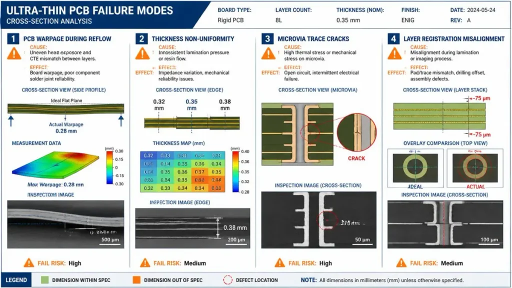
4 Critical Ultra-Thin PCB Failure Modes and Quality Inspection Analysis
1. Warpage and Bow Beyond SMT Tolerance
Copper (CTE ~17 ppm/°C) and FR-4 (CTE 45–55 ppm/°C) expand at different rates during reflow. In a 1.6 mm board, this mismatch is absorbed by the substrate mass. In a 0.20 mm board, it manifests as bow or twist that prevents proper solder paste printing. IPC-6012 allows ≤0.75% warpage for boards under 0.6 mm, but many SMT lines struggle above 0.5%.
Hongda Circuit mitigation: Symmetric stack-up design, copper thieving on sparse layers, LAUFFER vacuum lamination with zone-controlled pressure, and post-etch stress-relief baking. We ship thin boards in rigid support frames and can supply flatness measurement data per IPC-TM-650 Method 2.4.22 on request.
2. Thickness Non-Uniformity Across the Panel
A 0.20 mm board with ±0.02 mm variation is effectively 0.18–0.22 mm. If your connector or shielding design assumes a uniform 0.20 mm, that variation creates mechanical interference or gaps. The root cause is usually uneven lamination pressure or resin flow during cure.
Hongda Circuit mitigation: Real-time pressure profiling on every lamination cycle, and 9-point thickness measurement on every FAI lot.
3. Microvia and Fine-Line Yield Loss
In ultra-thin HDI, dielectric layers may be only 25–40 μm. A laser drill that is 5 μm off-center punches into the next copper layer, creating a short. A trace that is 3 μm under-etched opens under thermal stress. These defects do not always show up in electrical test; they are latent reliability risks.
Hongda Circuit mitigation: Mitsubishi UV/CO₂ laser drilling with ±5 μm positional accuracy, automated optical alignment for layer-to-layer registration within ±10 μm, and mSAP processing that eliminates subtractive etching undercut. Every microvia lot receives 3D X-ray inspection on our Nordson DAGE system.
4. Layer-to-Layer Registration Drift
As layer count increases and core thickness decreases, the cumulative registration error across 4–8 layers can exceed the annular ring design margin. This is especially critical for fine-pitch BGA pads on ultra-thin boards where the pad diameter may be only 0.20 mm.
Hongda Circuit mitigation: LDI imaging with ±1.5 μm accuracy, automated optical registration on every lamination cycle, and pre-drilled alignment holes that are optically verified before the next layer is laminated.
5.2. Documentation Buyers Should Require on Every Shipment
Do not accept a box of boards with a packing list. Demand a data package that includes:
- First Article Inspection (FAI) Report: Dimensional measurements at critical features, thickness at 9 points, trace width on test coupon.
- Cross-Section Photomicrographs: Via wall quality, copper thickness, dielectric integrity, and annular ring measurement.
- Electrical Test Report: 100% netlist verification or flying probe data, including impedance sweep if controlled impedance is specified.
- AOI and X-Ray Reports: Defect maps, void analysis in plated through-holes and microvias.
- Reliability Test Data (if applicable): Thermal shock (e.g., -65 °C to +150 °C, 1000 cycles), bend test for flexible sections, or IST (Interconnect Stress Test) for via reliability.
- Material Certification: RoHS/REACH compliance, UL flammability rating, and material lot traceability.
At Hongda Circuit, these reports are generated automatically by our quality management system and are available as PDF downloads within 24 hours of shipment.
5.3. Contract Terms That Protect Your Yield and Timeline
- Acceptance Criteria: Reference IPC-6012 Class 3 or 3A, but add project-specific clauses (e.g., “Thickness variation shall not exceed ±5% of nominal at any measured point”).
- Defective Material Policy: Define the supplier’s obligation for rework, replacement, or credit. For ultra-thin boards, rework is often impossible; replacement is the only remedy.
- Delivery Penalty / Incentive: A 1% per week late-delivery penalty (capped at 10%) and a 0.5% per week early-delivery bonus. This aligns incentives without being punitive.
- IP Protection: Non-disclosure agreement (NDA) covering Gerber files, stack-up designs, and test data. For medical and defense projects, add ITAR or equivalent data-handling clauses.
- Annual Quality Review: For volume programs, require a quarterly business review (QBR) with yield trends, corrective action logs, and continuous improvement initiatives.
6. How to Get a Quote Now: Streamlined RFQ Channels at Shenzhen Hongda Circuit
You have read the framework. You know the price ranges, the RFQ fields, and the quality gates. The next step is to send your specification and receive a manufacturability review and firm quote.
6.1. Online RFQ Form—What to Include for a 24-Hour Response
Our online RFQ portal at www.pcbkr.com is configured for ultra-thin PCB inquiries. To receive a response within 24 hours, include:
- Company name, contact person, and direct email/phone
- Project type: Prototype / Small Batch / Volume Production
- Key parameters: Board thickness, layer count, board dimensions, quantity, and target delivery date
- File upload: Gerber/ODB++ files, stack-up drawing, drill file, and impedance table (if applicable)
- Special requirements: Material preference, surface finish, quality standard (IPC Class 2/3), and any reliability testing needs
Our engineering team does not auto-generate quotes from a calculator. Every ultra-thin PCB RFQ is reviewed by a process engineer who checks:
- Can we hold the thickness tolerance with our current lamination parameters?
- Does the trace/space require mSAP or standard subtractive etching?
- Is the via aspect ratio feasible for the target thickness?
- Is the copper distribution symmetric enough to control warpage?
If we find a risk, we flag it in the quote response with a recommended alternative. This DFM-first approach prevents the surprises that derail projects.
6.2. Direct Email / WhatsApp / WeChat Inquiry Templates
Short-Form Template (for initial contact):
Subject: Ultra-Thin PCB RFQ – [Your Company] – [Project Name]
Hi Hongda Circuit Team,
We are sourcing an ultra-thin PCB for a [wearable medical device / foldable consumer product / automotive sensor module]. Key parameters:
- Thickness: [e.g., 0.20 mm ±0.02 mm]
- Layer count: [e.g., 4-layer]
- Trace/space: [e.g., 3 mil / 3 mil]
- Material: [e.g., FR-4 TG170 or specify if unsure]
- Surface finish: [e.g., ENIG]
- Quantity: [e.g., 50 pcs prototype + 2,000 pcs volume]
- Delivery: [e.g., prototype by Sept 15, 2026; volume by Oct 30, 2026]
- Destination: [e.g., FOB Shenzhen or DDP Los Angeles]
Gerber and stack-up files are attached. Please confirm capability fit and provide a firm quote with lead time and NRE breakdown.
Best regards, [Your Name] [Title] [Company]
Long-Form Template (for complex builds):
Subject: Custom Ultra-Thin HDI PCB – Detailed RFQ – [Project Name]
Hi Hongda Engineering Team,
Please find attached the complete specification package for our custom ultra-thin PCB requirement:
- Gerber files (RS-274X) and ODB++ archive
- Stack-up table with core/prepreg thicknesses and copper weights
- Drill chart (mechanical and laser microvias)
- Impedance control table (single-ended and differential)
- Outline drawing with panelization notes
- Quality standard: IPC-6012 Class 3
- Testing requirements: 100% electrical test, AOI, cross-section on 2 panels per lot
Target: 0.35 mm total thickness, 4-layer, 2 mil/2 mil traces, laser microvias (0.075 mm), ENIG finish. Quantity: 10 pcs prototype, 500 pcs pilot run, 5,000 pcs annual volume. Delivery: Prototype by [date]; volume ramp starting [date]. Shipping: DDP [your warehouse address].
We require FAI approval before volume release. Please include FAI data package pricing and lead time in your response.
We are particularly interested in your mSAP capability for the 2 mil/2 mil traces, and your experience with M9-grade CCL if this design requires low-loss material.
Best regards, [Your Name]
6.3. Our Service Commitment: Response Times and Engineering Escalation
- Inquiry Response: 30 minutes during business hours (China time, UTC+8) for all RFQs submitted through our website or to sales@pcbkr.com.
- Engineering Evaluation: 1 hour for DFM review on standard ultra-thin builds; 4 hours for complex HDI or rigid-flex designs.
- Quote Validity: 30 days from issuance, locked to the submitted Gerber revision.
- Technical Support: 24-hour engineering support during prototype debug. Direct access to our process engineers via email, WhatsApp, or WeChat.
- Prototype-to-Production Handoff: Dedicated project manager assigned at FAI approval, responsible for SPC monitoring, delivery scheduling, and quarterly business reviews.
Ultra-Thin PCB Sourcing FAQ: What Procurement Teams Ask Before Choosing a Supplier
What is the minimum thickness you can manufacture for a multilayer ultra-thin PCB, and what tolerance can you hold?
For mass production, we reliably fabricate 4-layer ultra-thin PCBs at 0.35 mm total thickness and 6-layer at 0.60 mm, maintaining IPC-6012 Class 3 flatness and ±0.05 mm thickness tolerance. For prototypes, we have delivered 2-layer boards at 0.15 mm and single-layer at 0.10 mm. Below 0.20 mm, we switch to vacuum-carrier handling and mSAP imaging to protect trace integrity. The key constraint is not the material; it is the lamination pressure uniformity and post-etch stress relief. If your design requires 0.10 mm 4-layer, we can evaluate it, but it will likely require SLP-grade processing with electroplated copper pillars rather than conventional etched traces.
How do you control warpage on ultra-thin PCBs during reflow assembly, and what data can you provide to prove it?
We attack warpage at three stages. Design stage: Our DFM team verifies copper balance and stack-up symmetry, recommending dummy fill or thieving patterns on sparse layers. Fabrication stage: Our LAUFFER vacuum lamination system uses zone-controlled pressure and gradual thermal ramps (not step changes) to cure resin without trapping stress. Post-etch baking removes residual mechanical stress from the copper foil. Delivery stage: We ship thin boards in rigid support frames and can supply flatness measurement data per IPC-TM-650 Method 2.4.22 on every FAI lot. For critical jobs, we also provide Cpk data on thickness uniformity across the panel.
Can you manufacture ultra-thin PCBs with controlled impedance for high-speed signals, and how do you ensure accuracy on thin dielectrics?
Yes. Impedance control on thin substrates is more sensitive than on standard boards because dielectric thickness directly affects characteristic impedance. A 5 μm variation in trace width can shift impedance by 2–3 Ω—unacceptable for 224 Gbps PAM4 channels. We use mSAP for near-vertical trace sidewalls (straightness ≥99%), LDI for ±1.5 μm imaging accuracy, and Polar impedance testing on every coupon. For ultra-thin high-speed designs, we target ±5% impedance tolerance and can provide TDR (Time Domain Reflectometry) sweep data on request. Our M9-grade CCL and Megtron 7/8 material inventory supports designs up to 224 Gbps.
What is the typical lead time for ultra-thin PCB prototypes versus volume production, and what can cause delays?
Prototypes (5–50 pcs): 5–7 working days for 2–4 layer standard ultra-thin; 10–12 days for HDI or rigid-flex. Volume (1,000+ panels): 2–3 weeks for standard ultra-thin; 4–5 weeks for Any-Layer HDI with M9 materials. The most common delays are not factory capacity; they are buyer-side specification changes, incomplete Gerbers, or material unavailability. We stock thinned FR-4 cores, high-Tg laminates, and M9-grade CCL to eliminate material lead time. Expedited lanes are available for medical and automotive emergency builds. The best way to protect your timeline is to lock your stack-up and Gerbers before submitting the RFQ.
How do I know if my design needs an ultra-thin rigid PCB or an ultra-thin flexible PCB, and what is the cost difference?
If your product requires static bending only during installation (e.g., a camera module that flexes once into a housing), an ultra-thin rigid PCB at 0.2–0.4 mm is usually sufficient and more cost-effective. If the circuit must dynamically flex repeatedly—wearables, foldable phones, robotic joints—you need a polyimide-based ultra-thin flexible PCB or a rigid-flex hybrid. The cost gap is significant: a 2-layer ultra-thin rigid PCB prototype runs $40–$150, while a comparable ultra-thin flex prototype with PI substrate and coverlay runs $80–$250 due to material cost and the coverlay lamination process. Send us your mechanical envelope, bend radius, and required flex cycles; our engineers will recommend the stack-up and material set that balances performance, reliability, and unit cost.
About Shenzhen Hongda Circuit Technology Co., Ltd.
Shenzhen Hongda Circuit Technology Co., Ltd. (trading as PCBkr) has manufactured precision interconnects from our Baoan, Shenzhen facility since 1999. We are not a broker. We own every critical process step in-house, from LDI imaging and laser drilling to vacuum lamination, mSAP plating, and X-ray inspection.
Key Certifications: ISO 9001:2026 | IATF 16949 (Automotive) | AS9100D (Aerospace) | IPC-6012 Class 3/3A | ISO 13485 (Medical Device — dedicated production lanes available)
Advanced Equipment: SCREEN Ledia LDI | Mitsubishi UV/CO₂ Laser Drilling | LAUFFER Lamination System | Nordson DAGE X-Ray | XRF Spectrometers | Multi-Chamber Inline PVD
Material Inventory: M9-Grade CCL | Megtron 7/8 | Rogers RO4350B / RT5880 | Taconic | Panasonic M6/M7 | Liquid Crystal Polymer (LCP) | Thinned FR-4 Cores
Capability Snapshot:
- Minimum rigid thickness: 0.10 mm (1L) / 0.15 mm (2L) / 0.35 mm (4L)
- Minimum flex thickness: 0.08 mm (production) / 0.05 mm (prototype)
- Fine-line capability: 8 μm/8 μm (mSAP/SLP) / 20 μm/20 μm (standard ultra-thin)
- Microvia: Blind 0.05 mm / Buried 0.15 mm (production); Blind 0.02 mm (prototype)
- Layer count: Up to 28 layers (production) / 78 layers (prototype)
- High-speed signaling: 224 Gbps PAM4 qualified
Contact: sales@pcbkr.com | www.pcbkr.com | WhatsApp / WeChat: Available on request
Next Step: Email your Gerbers and stack-up requirements. Our engineering team will return a manufacturability review and firm quote within 24 hours.
About Author
David Chen https://www.linkedin.com/in/pcbcoming
David Chen boasts an extensive professional background in PCBA manufacturing, PCBA testing, and PCBA optimization, with specialized expertise in high-precision PCBA fault analysis and rigorous PCBA reliability testing. The author has worked with high-layer-count server PCB fabrication, ultra-low-loss backplane stackups, and thermo-mechanical reliability optimization for AI infrastructure projects involving 112G and 224G PAM4 architectures. Skilled in complex circuit design and cutting-edge advanced PCB manufacturing processes, he delivers solutions that elevate product durability and performance across industrial applications. His technical articles focusing on PCBA manufacturing workflows and testing methodologies are widely cited by industry peers, research institutions, and technical platforms, solidifying his reputation as a recognized technical authority in the global circuit board manufacturing sector.