
Ultra-Thin PCB Manufacturer: 0.1–0.3 mm Rigid & Rigid-Flex PCBs for Compact Electronics
Shenzhen Hongda Circuit Technology Co., Ltd. manufactures ultra-thin PCBs down to 0.10 mm finished thickness, supporting fine-line 4/4 mil, laser microvias as small as 0.10 mm, and fast-turn prototypes to mass production. If your design team is fighting for every tenth of a millimeter inside a wearable housing, a medical probe, or a foldable consumer device, board thickness is no longer a specification—it is the constraint that determines whether the product ships on time.
Most ultra thin PCB manufacturers can quote 0.20 mm. Few can hold ±0.03 mm tolerance across a 500 × 500 mm panel after lamination, routing, and surface finish. Fewer still can do it repeatedly at volume. At Hongda Circuit, we built our thin-board workflow around the reality that sub-0.30 mm substrates behave differently at every process step: they warp during pressing, they shift during imaging, and they crack during depaneling. Our equipment and process controls are calibrated specifically for that reality.
What Defines an Ultra-Thin PCB? (And Why Most Thin PCB Suppliers Get It Wrong)
An ultra-thin PCB is generally classified as any rigid or rigid-flex board with a finished thickness between 0.10 mm and 0.30 mm. That range sounds narrow, but the manufacturing window collapses quickly once you drop below 0.25 mm. Standard FR4 laminates, subtractive etching, and mechanical drilling—the backbone of conventional PCB fabrication—start to produce unacceptable scrap rates.
The first failure point is warpage. A 0.10 mm core has almost no structural rigidity. During hot pressing, differential resin flow and copper coverage imbalances cause the panel to bow. If the thin PCB manufacturer does not use vacuum lamination with programmable pressure profiling, the board leaves the press curved. You receive parts that cannot sit flat during SMT assembly.
The second failure point is microvia quality. A 0.10 mm laser-drilled hole in a 0.10 mm core is essentially a through-hole. Miscontrol of pulse energy or desmear chemistry creates barrel cracks or resin smear that blocks plating. We see this frequently when buyers switch from a standard 1.6 mm board shop to a generalist supplier claiming ultra-thin PCB fabrication capability without dedicated laser parameters.
The third failure point is layer-to-layer registration. On multilayer thin PCBs, the coefficient of thermal expansion (CTE) mismatch between ultra-thin cores and copper foil becomes significant. Without automatic optical alignment (AOI) and X-ray punch systems, inner-layer shift exceeds 75 μm. That breaks fine-line connectivity and impedance targets.
At Hongda Circuit, we treat ultra-thin PCB manufacturing as a specialty, not a scaled-down version of standard board production.
Ultra-Thin PCB Manufacturing Capabilities at Hongda Circuit
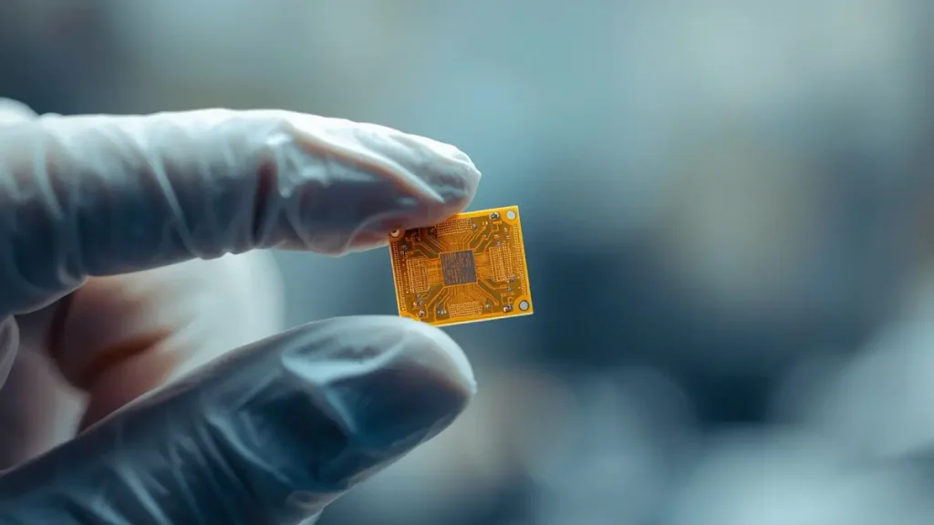
0.10mm Amber Polyimide Flexible PCB (FPC) Quality Inspection at Hongda Circuit
Our capability table is built from actual production data, not theoretical limits. Every parameter listed below has been validated in active jobs for wearables, medical, and consumer OEMs.
| Specification | Capability |
|---|---|
| Base Material | FR-4 Tg130 / Tg170 / Tg180 (ultra-thin cores); halogen-free available |
| Board Thickness | 0.10 mm – 0.30 mm |
| Copper Thickness | 0.5 oz / 1 oz / 2 oz / 3 oz (outer); 0.5 oz / 1 oz (inner) |
| Surface Finish | ENIG, OSP, ENEPIG, HAL-LF |
| Solder Mask | Bare / White / Black / Blue / Green / Red |
| Silkscreen | White / Black |
| Minimum Via Size | 0.10 mm laser microvia |
| Minimum Trace/Space | 4/4 mil |
| Outline Processing | CNC routing, punching, V-cut, laser depaneling |
| Maximum Panel Size | 500 × 500 mm or 1000 × 350 mm |
| Minimum Panel Size | 3.5 × 3.5 mm |
| Minimum Single Piece | 25 × 25 mm |
| Packing | Vacuum packing with desiccant and humidity indicator |
| Prototype Lead Time | 7–9 days |
| Mass Production Lead Time | 8–10 days |
We do not list capabilities we cannot guarantee. If your design calls for 3/3 mil on 0.10 mm, we will review the stack-up and copper distribution first. Ultra-thin PCB prototyping is only useful if the prototype actually reflects what the mass-production line can repeat.
Advanced Equipment & 2026 Manufacturing Technologies Behind Our Ultra-Thin PCBs
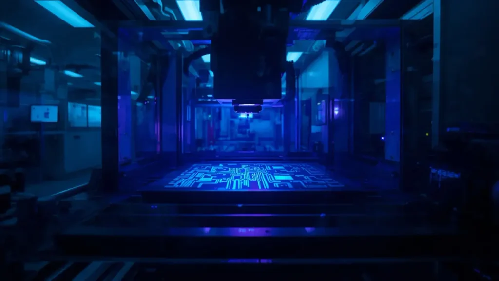
LDI Laser Direct Imaging Machine for Sub-50μm Ultra-Thin PCB Manufacturing at Hongda Circuit
The difference between a generalist board shop and a true ultra thin PCB manufacturing company is capital investment in equipment that addresses the physics of thin substrates. In 2026, these are the technologies that separate reliable suppliers from catalog vendors.
Laser Direct Imaging (LDI) for Sub-50 μm Trace Accuracy
We replaced conventional film-based photolithography with Laser Direct Imaging (LDI) for all ultra-thin jobs. LDI writes the resist pattern directly using a UV laser, eliminating film stretching and registration errors. On 0.10 mm cores, where mechanical handling already introduces flex, removing the film alignment step improves layer-to-layer registration by approximately 40 %. For designs at 4/4 mil—and tighter—LDI is not optional. It is the baseline.
Vacuum Lamination with Programmable Pressure Profiling
Our vacuum lamination presses operate at low-pressure, high-temperature profiles specifically developed for ultra-thin core stacks. Standard presses apply uniform pressure that crushes 0.10 mm prepreg and causes resin starvation. Our programmable system ramps pressure in three stages, maintaining dielectric thickness within ±5 % even on asymmetric copper builds. This directly controls the impedance consistency that RF and high-speed digital designers demand from their thin PCB supplier.
UV Laser Microvia Drilling & Plasma Desmear
We use UV laser drills for 0.10 mm microvias. The shorter wavelength produces cleaner hole walls with minimal glass-fiber protrusion on ultra-thin FR4 cores. After drilling, a plasma desmear cycle removes resin smear from the microvia base without over-etching the thin copper foil. The result is a plated microvia with >20 % copper wrap thickness and zero barrel cracks under thermal cycling.
Automated Optical Inspection (AOI) on Flexible Substrates
Because ultra-thin boards flex under their own weight, standard flat-bed AOI systems generate false calls. Our inspection line uses tension-controlled conveyor AOI that maintains planar stability during scanning. We catch opens, shorts, and insufficient annular rings down to 3 mil trace width without damaging the panel.
Industries We Serve: Ultra-Thin PCB Applications That Demand Zero Failure
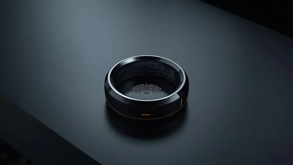
Ultra-Thin Flexible PCB Application in Smart Wearables & Rings
Buyers searching for an ultra thin PCB manufacturer usually fall into four categories. Each has a different tolerance for risk, but all share one requirement: the board cannot fail because it was too thin to manufacture correctly.
Wearables & Smart Accessories
Smart rings, health-monitoring bands, and AR glasses leave less than 1.5 mm of internal height for the entire electronics stack. Our 0.10 mm rigid-flex PCBs route signals across hinge zones while maintaining bend-radius compliance. We ship these in vacuum-sealed trays because a 0.15 mm board creases if you look at it wrong during transport.
Medical Implants & Portable Diagnostic Equipment
Implantable modules and handheld ultrasound probes require biocompatible surface finishes (ENEPIG) on thin substrates. The challenge is not just thickness—it is the combination of thinness + reliability + traceability. We provide lot-controlled material certificates and microsection reports for every medical thin-board job.
Ultra-Slim Consumer Electronics & IoT Sensors
Tablets, e-readers, and smart tags use thin multilayer PCBs (4–8 layers in 0.20–0.30 mm) to pack DDR routing and power management into minimal Z-height. Our DFM team reviews stack-ups for crosstalk and power-plane integrity before fabrication, because redesigning an 8-layer thin board after the first prototype costs more than the entire production run.
The Procurement Reality: 5 Pain Points Buyers Face With Thin PCB Suppliers
If you are a procurement manager or hardware lead evaluating an ultra-thin PCB manufacturer, you have probably encountered at least three of the following problems. We built our workflow to eliminate them.
1. Warpage that kills SMT yield. A 0.15 mm board with 0.3 mm bow cannot be pick-and-placed reliably. We control flatness to <0.5 % through vacuum lamination and post-press stress relief.
2. Inconsistent lead times between prototype and volume. Some shops quote 5 days for prototypes using manual methods, then discover their volume line cannot replicate the result. Our 7–9 day prototype and 8–10 day mass production schedules use the same equipment and same process recipe. No surprises.
3. Hidden DFM issues discovered too late. A trace routed over a void in a thin core creates an open after pressing. We run DFM checks on every ultra-thin PCB design before CAM, flagging copper balance, microvia aspect ratio, and solder-mask dam violations.
4. Damage during shipping. Thin boards snap in standard cardboard separators. We use vacuum-packed anti-static bags with foam inserts and humidity indicators. For 0.10 mm single pieces, we ship in panel form with laser depaneling instructions.
5. No engineering support for impedance or stack-up optimization. Buyers often know they need 50 Ω, but the stack-up to achieve it on 0.15 mm with 4 layers is not obvious. Our engineers provide pre-production stack-up modeling and impedance tolerance analysis (±3 % for high-precision jobs).
Why OEMs Choose Hongda as Their Ultra-Thin PCB Manufacturing Partner
From 7-Day Prototype to 8-Day Mass Production
Speed only matters if the first article is correct. Our prototype line runs on the same LDI, laser drill, and vacuum press equipment as our volume line. When you approve the prototype, we do not re-qualify the process. We scale the panel count. That is why our thin PCB mass production lead time stays at 8–10 days even for 0.10 mm, 4-layer builds.
DFM Review Before Fabrication Starts
Every quote request for ultra-thin PCB fabrication includes a complimentary DFM report. We check:
- Copper balance across the panel (critical for warpage)
- Microvia aspect ratio (target <0.8:1 on 0.10 mm cores)
- Solder-mask dam width on fine-pitch pads
- V-score residual thickness on fragile boards
You get the report before you pay. If the design is not manufacturable at yield, we tell you immediately.
Vacuum Packing & Damage-Free Global Shipping
Our standard packing for ultra-thin rigid and rigid-flex PCBs includes vacuum sealing, desiccant, humidity indicator cards, and custom foam fixtures for single pieces below 50 × 50 mm. We have shipped 0.10 mm boards to Germany, the United States, and Japan with zero transit damage over the last 24 months.
Ultra-Thin PCB Design Guidelines (From Our Engineering Team)
These are not generic rules. They are constraints we enforce in our DFM checks to protect your yield.
Stack-Up Recommendations for 0.10–0.30 mm Boards
Use symmetric copper coverage. A 0.10 mm, 2-layer board with 2 oz on one side and 0.5 oz on the other will bow. For 4-layer builds, mirror the outer copper weights. Choose Tg170 or Tg180 cores if the assembly profile exceeds 245 °C; standard Tg130 resin softens and causes measling on thin substrates.
Trace/Space & Via Rules to Avoid Delamination
Keep trace/space at ≥ 4/4 mil for production stability. If your design requires 3/3 mil, we can evaluate it, but the cost increases and the yield drops. For vias, use 0.10 mm laser microvias with a 0.25 mm capture pad. Smaller pads increase annular ring fracture risk during depaneling.
Panelization & Depaneling for Fragile Thin Boards
Avoid large single-piece outlines on 0.10 mm material. We recommend tab-routing with 2 mm tabs or laser depaneling for irregular shapes. V-scoring is acceptable for 0.20 mm and above, but the residual web must be ≥ 0.10 mm to prevent snapping during separation.
Quality Assurance for Ultra-Thin PCBs
Thickness Tolerance & Warpage Control
We measure finished thickness at five points per panel using a digital micrometer. Target: ±0.03 mm on 0.10–0.20 mm boards. Warpage is checked on a granite surface plate under standardized lighting. Reject limit: <0.5 % for SMT-grade boards.
Electrical Testing & Microsection Analysis
Every ultra-thin PCB receives 100 % electrical testing (flying probe or fixture, depending on volume). For first articles and quarterly process audits, we perform microsection analysis to verify copper wrap thickness, dielectric layer thickness, and microvia barrel integrity.
Request a Quote for Your Ultra-Thin PCB Project
Upload your Gerber files and stack-up notes through our inquiry portal at www.pcbkr.com, or email ( sales@pcbkr.com)our engineering team directly. We return DFM feedback and pricing within 24 hours for standard builds. If you are comparing ultra thin PCB manufacturers for a new wearable, medical, or IoT program, start with a supplier that owns the equipment, the process, and the thin-board expertise—not one that treats 0.10 mm as a tolerance exception.
FAQ: What Procurement Teams Ask Before Choosing an Ultra-Thin PCB Manufacturer
What is the thinnest PCB thickness your factory can reliably manufacture and ship without damage?
We routinely manufacture and ship rigid and rigid-flex PCBs at 0.10 mm finished thickness. Below 0.10 mm, we move to flexible polyimide constructions. All 0.10 mm shipments leave our facility in vacuum-sealed, foam-supported packaging. We have not recorded a transit damage claim on thin-board shipments in the past two years.
How do you control warpage on 0.1 mm ultra-thin PCBs during high-temperature lamination?
We use vacuum lamination presses with programmable low-pressure profiling, symmetric stack-up enforcement in DFM, and post-press stress-relief baking. Copper balance is verified before the job enters CAM. These four controls keep warpage under 0.5 % on panels up to 500 × 500 mm
What is the realistic lead time from prototype approval to mass production for thin PCBs?
7–9 days for prototypes; 8–10 days for mass production. Because our prototype and volume lines share identical LDI, laser drill, and vacuum press equipment, there is no re-qualification delay when you move from first article to production.
Can you support impedance control and HDI microvias on boards below 0.20 mm?
Yes. We model controlled-impedance traces on 0.10–0.30 mm substrates using Polar Instruments stack-up software, targeting ±3 % tolerance for high-precision jobs. Our 0.10 mm laser microvias support any-layer HDI in builds up to 6+n+6, provided the aspect ratio stays within process limits.
Do you provide DFM review before I place a purchase order for ultra-thin PCBs?
Absolutely. Every quote request receives a complimentary DFM review covering copper balance, microvia feasibility, solder-mask dam width, and panelization strategy. We flag manufacturability risks before you commit to tooling. This prevents the costly scenario of receiving prototypes that cannot scale to volume.
About Author
David Chen https://www.linkedin.com/in/pcbcoming
David Chen boasts an extensive professional background in PCBA manufacturing, PCBA testing, and PCBA optimization, with specialized expertise in high-precision PCBA fault analysis and rigorous PCBA reliability testing. The author has worked with high-layer-count server PCB fabrication, ultra-low-loss backplane stackups, and thermo-mechanical reliability optimization for AI infrastructure projects involving 112G and 224G PAM4 architectures. Skilled in complex circuit design and cutting-edge advanced PCB manufacturing processes, he delivers solutions that elevate product durability and performance across industrial applications. His technical articles focusing on PCBA manufacturing workflows and testing methodologies are widely cited by industry peers, research institutions, and technical platforms, solidifying his reputation as a recognized technical authority in the global circuit board manufacturing sector.