7th-Order Arbitrary Interconnection HDI PCB: Buried/Blind Via Circuit Board Manufacturing Guide
About the Author & Technical Reviewer
Written and technically reviewed by the PCBKR Engineering Team, Shenzhen Hongda Circuit Technology Co., Ltd. (www.pcbkr.com). Our senior process engineers have more than 15 years of hands-on experience in HDI fabrication — from first-generation 1+N+1 build-ups to today’s mSAP-based any-layer HDI boards for AI servers, smartphones and aerospace electronics. Every process claim in this article reflects equipment we actually operate on our factory floor (SCREEN Ledia LDI, Mitsubishi UV/CO₂ laser drilling, Lauffer lamination, automated pulse plating, X-ray and microsection labs) and is cross-checked against IPC-2226, IPC-6016, IPC-6012 and IPC-A-600 requirements.
Editorial standard: this page follows E-E-A-T principles — demonstrated Experience (real production cases), Expertise (senior engineering authorship), Authoritativeness (IPC standards, published industry data, verifiable equipment list) and Trustworthiness (no unverified capability claims; every geometry number is a qualified production value, not a marketing minimum).
What Is a 7th-Order Arbitrary Interconnection HDI PCB? (7th-Order HDI Circuit Board Explained)
A 7th-order arbitrary interconnection HDI PCB — also called a 7th-order HDI circuit board, 7-step HDI PCB or high-order any-layer HDI PCB — is an advanced multilayer circuit board built from repeated HDI build-up structures, in which laser-drilled microvias, blind vias and buried vias connect any layer to any other layer (Every Layer Interconnect, ELIC). The result is extremely high routing and I/O density inside a very small footprint, which is exactly what modern fine-pitch BGAs, SoC modules and AI accelerator boards demand.
Let us be precise, because this is where many datasheets mislead buyers: “7th-order” is not a single globally unified IPC class name. It is defined by the actual stackup and build-up structure — typically a core with multiple (in our production practice, six or more) sequential microvia build-up steps on each side, e.g. a 6+N+6 or 7+N+7 style construction — not by a marketing label. Two boards both sold as “7th-order HDI” can differ enormously in lamination cycles, microvia stack strategy and reliability margin. The only way to qualify a 7th-order HDI buried/blind via circuit board is: Stackup → Lamination → Via Structure → Drilling → Plating. If a supplier cannot show you this chain, the order number is meaningless.
| Parameter | Specification |
| HDI Structure | High-order / arbitrary interconnection (ELIC / any-layer) |
| Interconnection | Blind vias / buried vias / laser microvias / stacked & staggered microvias |
| Build-Up Method | Sequential build-up (SBU) with multiple lamination cycles |
| HDI Order | Defined by actual stackup (e.g., 6+N+6, 7+N+7); verified in DFM review |
| Layer Count | Project-specific; qualified up to high layer counts |
| Material | High-Tg FR-4, low-Dk/low-Df, RF laminates — project-specific |
| Laser Microvia | UV/CO₂ hybrid laser, depth-controlled, project-specific diameter |
| Impedance | Controlled per stackup; 100% TDR verification available |
| Quality Class | IPC Class 2 / 3 per IPC-6012 & IPC-6016; customer spec applies |
| Testing | AOI, X-ray, microsection, ET, impedance, thermal stress / cycling |
What Does “7th-Order” Mean in HDI PCB Manufacturing? (HDI Order, Step and Generation)
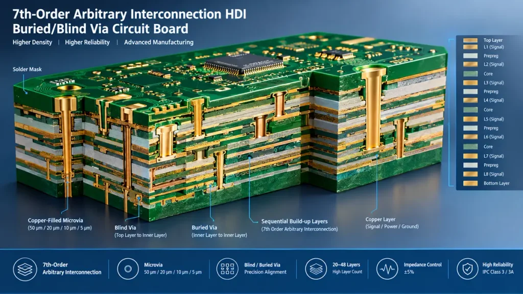
7th-order arbitrary interconnection HDI buried/blind via circuit board manufacturing structure by Hongda Circuit
What Is an HDI Build-Up Order?
HDI build-ups are described with the “order + core + order” notation. In 1+N+1, one microvia layer is added on each side of an N-layer core. In 2+N+2, two microvia layers are added per side; 3+N+3 adds three. Beyond roughly 3+N+3 we speak of higher-order or high-order HDI, and when microvias extend through the entire stackup to give any-to-any connectivity, the construction becomes Any-Layer HDI (ELIC) — the true meaning of a 7th-order arbitrary interconnection HDI PCB.
What Is the Difference Between HDI Order, Step and Generation?
Industry language is loose here, and procurement teams should insist on definitions. “Order” counts build-up layers per side (2+N+2 = order 2). “Step” is often used the same way by Asian factories (“7-step HDI”). “Generation” is used more in material and equipment marketing. Under IPC-2226, what matters is the construction Type: Types I–III cover single and dual build-up layers, while Types IV–VI cover passive-core, coreless and alternate constructions used in the highest-density any-layer boards. When you evaluate a 7th-order HDI circuit board, ask for the IPC type, the stackup drawing, and the number of lamination cycles — not the slogan.
Why Should the Actual Stackup Define the HDI Order?
Because the physics of the process chain is driven by the stackup, not the label. Each additional build-up cycle adds another exposure of every existing interface to lamination temperature and pressure, another registration opportunity, another laser-drill cycle and another plating cycle. Stackup determines lamination count; lamination count determines cumulative registration error; via structure determines drilling and filling strategy. IPC-2226 notes that cumulative z-axis registration errors grow significantly beyond two sequential stacks — which is precisely why high-order HDI requires X-ray-aligned registration, material shrinkage compensation and disciplined per-cycle process control. This is also why genuine 7th-order HDI capability cannot be claimed without sequential lamination, LDI imaging and hybrid UV/CO₂ laser drilling all in-house.
What Does Arbitrary Interconnection Mean in a 7th-Order HDI PCB? (Any-Layer / ELIC)
How Does Any-Layer Interconnection Work?
In arbitrary interconnection — ELIC (Every Layer Interconnect), the technical name behind “any-layer HDI” — microvias are extended through the entire board so a signal can transition from any layer to any other layer at almost any XY location. A 0.35 mm-pitch BGA can escape on the layer directly beneath it, instead of dog-boning through four routing layers. This is what makes 7th-order any-layer HDI the densest practical PCB interconnect technology short of IC substrates.
How Is Any-Layer HDI Different From Conventional HDI?
Conventional HDI (1+N+1, 2+N+2) constrains via placement and forces channel routing on designated layers. Any-layer HDI removes that constraint: via-in-pad plated over (VIPPO), stacked microvias and skip vias combine so the layout engineer routes the chip, not the board. The manufacturing price of that freedom is severe — every layer pair is now a via candidate, so registration, capture-pad design, copper fill and planarization must be controlled on every build-up, not just the outer ones.
When Is Arbitrary-Layer Interconnection Required?
- Fine-pitch BGA / LGA packages below ~0.4 mm pitch where escape channels are exhausted
- Multi-side, multi-die modules (SoC + memory + PMIC) on one substrate-sized board
- AI/HPC accelerator boards where thousands of high-speed I/O must break out from a large ASIC
- Miniaturized medical and wearable electronics where board area is the primary constraint
How Do Blind, Buried and Microvias Work in a 7th-Order HDI Buried/Blind Via Circuit Board?
Blind vias connect an outer layer to one or more inner layers without passing through the board; buried vias connect inner layers only, fully enclosed in the stackup; microvias are laser-drilled vias with a diameter of 150 µm or less, normally connecting only adjacent layer pairs — and it is the microvia that makes arbitrary interconnection economically possible. Stacked microvias sit directly on top of each other to save space; staggered microvias offset consecutive vias for lower reliability risk and lower cost.
| Via Type | Connection | Formation | Key Reliability Concern | Typical Use |
| Blind via | Outer → inner layer(s) | Laser (microvia) or controlled mechanical drill | Capture-pad annular ring after shrinkage | BGA escape, layer-pair transitions |
| Buried via | Inner → inner layers | Mechanical drill in sub-composite | Sub-composite registration before lamination | Power/ground grids, core routing |
| Microvia | Adjacent layers only | UV/CO₂ laser, depth-controlled | Aspect ratio ≤ ~0.75–1:1, void-free fill | Any-layer interconnect backbone |
| Stacked microvia | Vertical microvia column | Consecutive laser cycles + copper fill | Cumulative registration; weakest reliability link | Highest density, VIPPO |
| Staggered microvia | Offset consecutive vias | Consecutive laser cycles | Lower risk, slightly larger footprint | Default choice when density allows |
When Is Via-in-Pad Required?
When BGA pitch drops below ~0.4 mm, dog-bone fan-out consumes more space than exists between pads. Via-in-pad (filled, planarized and plated over — VIPPO) becomes mandatory. Every via-in-pad in a 7th-order HDI board must be filled and planarized; an unfilled via lets solder wick down the barrel and starves the joint. This single requirement is why via filling and planarization capability separates real high-order HDI manufacturers from assemblers of buzzwords.
What Is the Difference Between 7th-Order HDI and Conventional HDI?
| Feature | Conventional HDI (1+N+1 / 2+N+2) | Higher-Order HDI (3+N+3+) | 7th-Order / Any-Layer HDI |
| Build-up complexity | Low | High | Very high |
| Microvia layers | 1–2 per side | Multiple | Extensive / full ELIC |
| Lamination cycles | 2–3 | 4+ | Multiple sequential cycles, project-specific |
| Routing freedom | Moderate | High | Very high (any-layer) |
| BGA escape capability | ≤ ~0.5 mm pitch | ~0.4 mm pitch | ≤ ~0.35 mm pitch |
| Registration requirement | High | Very high | Critical — X-ray alignment per cycle |
| Typical imaging | Conventional or LDI | LDI required | LDI (mSAP-ready) required |
| Manufacturing complexity | Moderate | High | Very high |
Principle for buyers: use the lowest HDI order that reliably solves the routing problem. A 7th-order arbitrary interconnection HDI PCB is not “better” in the abstract — it is necessary only when lower orders provably fail, and it carries real cost and reliability process burden. A trustworthy high-order HDI PCB manufacturer will tell you honestly when 2+N+2 is enough.
When Does a PCB Need 7th-Order Arbitrary Interconnection? (Engineering Triggers)
When Is 1+N+1 or 2+N+2 No Longer Enough?
- BGA escape routing still fails after disciplined layer-pair assignment and dog-bone optimization
- Required layer count exceeds what sequential escape allows without via-in-pad everywhere
- Two high-pin-count devices must be routed through each other (crossing channel demands)
- Board size is fixed by the product enclosure and lower-order HDI cannot meet it
When Does BGA I/O Density Require Any-Layer Interconnection?
The quantitative trigger is pitch. Around 0.4 mm pitch, one via per pad with via-in-pad becomes the only escape strategy; around 0.35 mm and below, stacked microvias and ELIC are effectively mandatory for large-ball-count devices. If your flagship chip has 0.35 mm-pitch BGA and more than ~1,500 balls, plan for 7th-order-class HDI from day one — retrofitting it after layout is a redesign, not a revision.
How Does a 7th-Order HDI PCB Stackup Work? (7th-Order HDI Stackup)
A typical high-order stackup combines: (1) a mechanically drilled core or sub-composite with buried vias, (2) symmetric sequential build-up layers of thin dielectric (resin-coated copper or prepreg, commonly ~50–100 µm per build-up) with laser-drilled microvias, and (3) balanced signal/ground/power distribution with symmetric copper on both sides to control warpage.
Symmetric Stackup, Copper Balance and Dielectric Thickness
Warpage is the silent killer of high-order HDI. Every asymmetric ounce of copper and every unbalanced build-up converts directly into bow and twist at reflow, and warpage converts directly into misregistration at the next laser-drill cycle. Our stackup engineering rule at PCBKR: mirror copper weights layer by layer, keep build-ups symmetric about the core, and lock dielectric thickness distributions so impedance targets hold after every lamination. Dielectric thickness and copper roughness together define impedance — HVLP-class low-profile foil matters as much as resin content for 10–28 Gbps-class channels.
How Many Sequential Lamination Cycles Does a 7th-Order HDI PCB Require?
There is no honest fixed number — the cycle count is derived from the stackup: typically one cycle for the core, plus one per build-up layer (and additional cycles when buried-via sub-composites are pressed separately). A 7th-order-class board commonly passes through many more thermal exposures than a 2+N+2 board, which is exactly where most factories fail.
Why this is the #1 pain point: more build-up cycles mean more registration opportunities and greater process-control requirements. Each cycle adds z-axis material movement, resin flow variance and dimensional shrinkage. Controlling it requires X-ray-to-target registration per cycle, artwork shrinkage compensation updated from measured panel data, low-CTE high-Tg materials (Tg ≥ 170–180 °C recommended), and lamination presses with uniform temperature and pressure distribution. On our Lauffer lamination system, we profile each material lot and compensate artwork per cycle — this is the difference between a qualified 7th-order HDI manufacturer and one that quotes it.
How Are Microvias Manufactured in a 7th-Order HDI PCB? (Latest Process Technology)
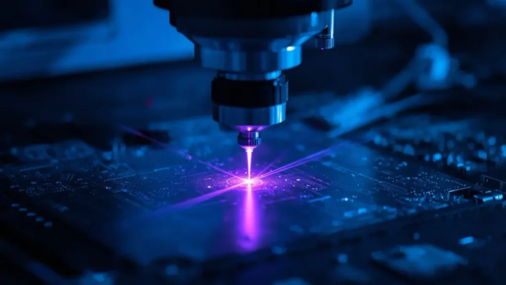
Laser microvia drilling process in the manufacturing of 7th-order arbitrary interconnection HDI buried/blind via circuit boards by Hongda Circuit
The microvia process chain is: Laser Drilling → Desmear → Electroless Copper (seed) → Electrolytic Pulse Plating → Via Fill → Planarization → Microsection / X-Ray Inspection.
Laser Drilling: UV/CO₂ Hybrid Is Now the Standard for High-Order HDI
CO₂ lasers ablate dielectric efficiently; UV lasers drill small, clean holes and handle copper-direct drilling. Hybrid UV/CO₂ platforms — such as the Mitsubishi Electric UV/CO₂ laser drilling systems we operate — give depth-controlled blind vias with stable diameter across glass-rich dielectrics. Beam positioning tolerance and per-pulse energy stability directly determine capture-pad capture rate after cumulative lamination shrinkage; on a 7th-order board, laser positional drift budget shrinks with every cycle, which is why mechanical drill platforms and aging CO₂-only lasers show sharply rising fallout on high-order work.
Desmear, Seed Copper and Pulse Plating
After drilling, smear removal (desmear) must clean the via barrel without attacking the thin capture interface. Electroless copper deposits the conductive seed; then pulse-reverse electroplating builds barrel and fill copper. Void-free filling of stacked microvias requires tight chemistry control and plating-current waveform management — continuous DC plating leaves center voids that become cracks under thermal cycling. This is why we run fully automated plating lines with pulse-reverse rectification and in-line chemistry monitoring rather than manual tank lines: in high-order HDI, the plating line is a reliability machine, not a cost center.
Via Fill, Planarization and Microsection
Copper-filled microvias are planarized to a flat surface so the next build-up (or the BGA pad) sees no dimple. We verify fill quality by microsection on production panels per IPC-TM-650 methods and by X-ray for stacked structures — because what you cannot see in a stacked microvia column is where your field failures will come from.
How Are Stacked Microvias Made Reliable in High-Order HDI? (Microvia Reliability)
What Causes Microvia Cracking?
The classic failure modes are: copper-fill center voids, barrel-corner cracking at the capture-pad interface, delamination at the dielectric/copper interface, and registration-induced partial land overlap. All are aggravated by thermal cycling — every reflow pass and every lamination cycle is a stress test of every microvia already in the board.
Engineering Controls That Actually Work
- Void-free copper fill via pulse-reverse electroplating with in-line chemistry control
- Via geometry discipline: aspect ratio ≤ ~0.75:1 per IPC-2226 guidance, tapered profiles, no flat-bottom vias
- Registration: X-ray alignment and measured artwork compensation on every lamination cycle
- Materials: high-Tg, low-CTE dielectrics to suppress z-axis expansion stress
- Inspection: microsection per IPC-TM-650, thermal stress and thermal cycling per IPC-6016 qualification logic
- Design hygiene: stagger microvias wherever density allows; stack only where the layout truly forces it
Field experience, stated plainly: in more than 15 years of HDI production, the majority of “mysterious” high-order HDI field failures we have been asked to analyze trace back to one of three causes — unmonitored plating chemistry drift, no per-cycle registration compensation, or a supplier quoting stacked-microvia boards without an X-ray program. All three are process-discipline failures, not bad luck.
What Materials Are Used for 7th-Order HDI PCBs?
| Requirement | Material Consideration |
| General high-order HDI | High-Tg FR-4 (Tg ≥ 170–180 °C) |
| High thermal stress / many lamination cycles | High-Tg, low-CTE laminates and prepregs |
| High-speed / AI-HPC channels | Low-Dk / low-Df systems (e.g., Megtron-class, ITEQ IT-180A / low-Df grades) |
| RF / mmWave layers | RF laminates (Rogers, Taconic) in hybrid stackups |
| Thin build-up layers | Thin dielectric / RCC, controlled thickness per build-up |
| Fine-line mSAP layers | Ultra-thin / HVLP low-profile copper foil |
| Via filling | CTE-matched fill systems; CTE mismatch at the fill interface is a known crack initiator |
Material note for 2026 procurement: several laminate families now explicitly guarantee multiple sequential lamination cycles and mSAP fine-line adhesion in their published data — specify the material by datasheet lamination-cycle rating, not by brand habit.
What Trace Width, Spacing and Microvia Dimensions Are Required for 7th-Order HDI?
An honest capability statement must separate three numbers: minimum demonstrated geometry, qualified production geometry, and recommended design geometry for high yield. The industry direction in 2026 is unambiguous: subtractive etching tops out around 50/50 µm for volume work, while mSAP (modified semi-additive process) with LDI imaging reaches 30/30 µm and below; laser microvias in high-volume HDI are now commonly 60–100 µm. Microvia capture pads must be sized for cumulative registration — IPC-2226-based practice allows for on the order of ±25–30 µm layer-to-layer tolerance after sequential cycles, so capture pads are commonly designed around 300 µm class for 100 µm vias in conservative high-order builds.
At PCBKR we qualify each geometry per stackup in DFM review; we do not publish a single “minimum line width” as a blanket promise, because on 7th-order HDI the correct minimum depends on copper weight, dielectric, aspect ratio and lamination cycle count. Minimum advertised geometry is never the same as qualified production geometry — treat any supplier who implies otherwise with suspicion.
How Do 2026 PCB Manufacturing Technologies Change What a 7th-Order HDI Manufacturer Can Deliver?
Four technology shifts define the current state of the art, and they directly determine whether a 7th-order arbitrary interconnection HDI buried/blind via circuit board is a qualified product or a quote on a website:
1. mSAP / SLP Processing Replaces Subtractive Etching for Fine Lines
mSAP plates copper onto a thin seed and flash-etches the seed away, eliminating the undercut that limits subtractive etching. Line/space of 30/30 µm and below — formerly IC-substrate territory — is now production-realistic for advanced HDI, and substrate-like PCB (SLP) technology is expanding from smartphones into automotive ADAS, IoT and wearables. For a 7th-order board, mSAP on the outer build-ups is often the only way to break out 0.35 mm-pitch packages.
2. LDI (Laser Direct Imaging) Replaces Film Exposure
Below ~50 µm features, film stretch and registration make artwork scaling a guess. LDI writes each panel directly from CAD with measured-panel scaling. Our SCREEN Ledia LDI systems expose fine build-up layers with the positional stability that high-order registration budgets demand; without LDI, sub-50 µm production on multi-cycle boards is luck, not process.
3. Hybrid UV/CO₂ Laser Drilling with Closed-Loop Depth Control
Depth-controlled blind microvias on thin dielectrics, drilled at high throughput with per-hole energy monitoring, are now the baseline for any-layer HDI — including ~60 µm-class blind vias for the densest mSAP builds.
4. X-Ray + Microsection Reliability Programs as Standard Qualification
IPC-2226 practice recommends X-ray for stacked microvia structures, and leading 2026 HDI facilities run CT/X-ray microvia inspection plus thermal cycling as routine qualification. A supplier without an X-ray story for stacked vias is disqualified for 7th-order work, full stop.
What Are the Main Manufacturing Challenges of 7th-Order HDI? (The Pain Points, Honestly)
Sequential lamination alignment and X-ray inspection quality control for 7th-order arbitrary interconnection HDI buried/blind via circuit boards by Hongda Circuit
After a decade and a half of building high-order HDI, here is our ranked list of where 7th-order projects actually hurt — and what separates factories that survive them from factories that quietly ship risk:
Pain Point #1: Cumulative Registration Across Sequential Lamination
This is the single biggest pain point in manufacturing a 7th-order arbitrary interconnection HDI circuit board. Every lamination cycle moves every layer already in the board. Mitigation: X-ray alignment per cycle, per-lot artwork compensation from measured shrinkage, symmetric stackups, and low-CTE materials. Equipment that makes the difference: X-ray drilling/registration systems, LDI with scaling, precision lamination presses. These registration requirements are not unique to 7th-order HDI; they are part of the broader high precision PCB manufacturing discipline covering layer registration, hole position, microvia alignment, dimensional tolerance and impedance control.
Pain Point #2: Stacked Microvia Reliability (Cracking, Voids, Delamination)
Each stacked column multiplies the plating quality requirement. Mitigation: pulse-reverse plating with monitored chemistry, microsection per IPC-TM-650, thermal cycling validation, and design rules that force staggering unless stacking is unavoidable.
Pain Point #3: Warpage and Copper Balance
Multi-cycle boards with asymmetric power planes bow; bowed boards misregister at laser drill. Mitigation: copper thieving and mirrored stackups enforced at DFM, Lauffer-class press uniformity, flatness measured per panel.
Pain Point #4: Fine-Line Yield on mSAP Layers
30/30 µm lines fail on resist adhesion, seed residue and etch chemistry drift long before they fail on paper. Mitigation: LDI imaging, controlled cleanroom panels, and AOI upgraded to ~25 µm-class resolution.
Pain Point #5: Yield Loss and Cost Multiplication
With many sequential cycles, a defect in the last cycle scrapes the value of every prior cycle. This is why 7th-order HDI pricing cannot follow standard PCB cost logic — and why DFM before fabrication is the highest-ROI activity in the program.
| Manufacturing Risk | Root Cause | Control at PCBKR |
| Registration error | Multiple build-up cycles, material shrinkage | X-ray registration + per-cycle artwork compensation |
| Microvia cracking / voids | Plating chemistry drift, poor fill | Pulse-reverse plating, in-line chemistry monitoring, microsection |
| Warpage | Stackup imbalance | Symmetric stackup design, Lauffer lamination uniformity |
| Fine-line defects | Imaging / etch variation | SCREEN Ledia LDI, mSAP process, high-resolution AOI |
| Delamination | Lamination / material CTE | High-Tg low-CTE materials, lamination profiling |
| Yield loss | Process complexity | DFM-first review, SPC, per-cycle inspection gates |
How Is a 7th-Order Arbitrary Interconnection HDI PCB Manufactured? (Process Flow)
Our production flow: Engineering & DFM Review → Stackup Engineering → Material Preparation → Inner-Layer Imaging (LDI) → Sub-Composite Lamination → Buried Via Drill / Plate → Sequential Build-Up Lamination → Laser Drilling (UV/CO₂ hybrid) → Desmear → Electroless Copper → Pulse Electroplating / Via Fill → Planarization → mSAP or Fine-Line Outer Processing → AOI → X-Ray → Surface Finish → Electrical Test → Impedance Test → Microsection / Final Inspection → Ship with full quality documentation.
Every step above is performed in-house at our Shenzhen facility — no outsourced laser drilling, no outsourced lamination. For high-order HDI, outsourced process steps are uncontrolled process steps.
How Are 7th-Order HDI PCBs Tested for Quality and Reliability?
- AOI on every circuit layer, upgraded resolution for mSAP fine lines
- X-ray inspection of stacked microvia structures and registration verification
- Microsection analysis per IPC-TM-650 (plating thickness, fill quality, interface integrity)
- Electrical testing (flying probe / fixture) on finished boards
- Impedance testing (TDR) on controlled-impedance coupons and boards
- Thermal stress (solder float / reflow simulation) and thermal cycling per qualification plan
- IPC-6016 microvia qualification logic applied to HDI constructions, with IPC-6012 and IPC-A-600 acceptance as applicable to the product class
Applicable standards depend on the PCB construction, product class and customer specification — any blanket claim that “one standard covers everything” is a red flag in supplier evaluation.
How Much Does a 7th-Order HDI PCB Cost? (Cost Model for Buyers)
| Cost Driver | Why It Moves Price |
| Layer count | Base material and process time scale directly |
| HDI order (build-up count) | Each order level adds lamination + laser + plating cycles |
| Sequential lamination cycles | The dominant cost multiplier in high-order HDI |
| Laser drilling | Hole count × cycles; microvia quantity is linear in cost |
| Microvia quantity & stacking | Stacked/filled vias add plating and planarization cost |
| Via filling (VIPPO) | Fill + planarize + inspect on every via-in-pad |
| Fine-line / mSAP processing | Yield-sensitive premium process |
| Material system | High-Tg / low-Dk / RF laminates multiply material cost |
| Testing & qualification | Microsection, X-ray, thermal cycling programs |
| Yield at order N | The hidden variable — quoted by weak factories as your risk |
| Panel utilization | Nesting efficiency and mixed-panel strategy |
How Can Engineers Reduce 7th-Order HDI PCB Cost Without Reducing Reliability?
- Use the lowest HDI order that reliably solves the routing problem — order is the biggest cost lever
- Stagger microvias instead of stacking wherever density permits; stacking is a last resort
- Reduce unnecessary build-up layers at DFM; one removed cycle removes a full process loop
- Optimize panel utilization early — panel nesting affects cost as much as layer count
- Select materials by electrical requirement, not by habit; hybrid stackups can cut cost sharply
- Avoid ultra-fine geometry where it buys nothing; every 10 µm of finer line has a yield price
- Apply DFM before fabrication: 80% of high-order HDI cost overruns are layout decisions made before anyone called the factory
Which Applications Use 7th-Order or Any-Layer HDI?
| Application | Main Density Driver | HDI Requirement |
| High-end smartphones / wearables | Footprint and thickness | Any-layer / ELIC, mSAP fine lines |
| AI servers / HPC accelerators | ASIC I/O count + 112G/224G channels | High-order HDI + low-loss materials + backdrill |
| SoC / FPGA systems | High I/O density | Microvia / stacked via HDI |
| High-density networking (800G/1.6T) | Dense interfaces + signal integrity | HDI + impedance control + low-Dk |
| Aerospace / defense | SWaP-C constraints | High-order HDI + reliability qualification |
| Medical electronics | Miniaturization + reliability | HDI + biocompatibility-grade processes |
What Should You Include in a 7th-Order HDI PCB RFQ?
- Design files: Gerber, ODB++ or IPC-2581, plus drill files
- Stackup requirements: layer count, core, prepreg, dielectric and copper thicknesses
- HDI requirements: target HDI order, via start/stop layers, blind/buried/microvia definitions, stacked vs. staggered strategy, via filling requirements
- Electrical requirements: impedance targets and tolerances, differential pairs, data rates, insertion-loss limits where applicable
- Quality requirements: IPC class, testing scope, microsection and reliability expectations
- Commercial requirements: prototype quantity, production quantity, annual volume, lead time
Send your 7th-order HDI PCB RFQ to PCBKR — response within 24 hours with engineering feedback, not just a price.
How Should You Qualify a 7th-Order HDI PCB Manufacturer? (Checklist)
The 7th-Order HDI Supplier Qualification Checklist
| # | Check | Pass Evidence |
| 1 | Qualified HDI order in production (not samples) | Cross-section library at your order level |
| 2 | Any-layer / ELIC capability | ELIC production boards + registration data |
| 3 | Laser drilling in-house | UV/CO₂ hybrid platforms, depth-control records |
| 4 | Sequential lamination in-house | Press list + cycle-count history on similar stackups |
| 5 | Microvia filling & planarization | Fill microsections, planarity measurements |
| 6 | Registration control | X-ray alignment + artwork compensation records |
| 7 | Reliability testing | Thermal cycling reports, microvia qualification |
| 8 | Quality certifications | ISO 9001; IATF 16949 / ISO 13485 / AS9100D / UL as applicable |
| 9 | Prototype-to-mass consistency | Same process route from prototype to volume |
| 10 | DFM engagement | Engineers who ask about your stackup, not just your PO |
Why Choose Shenzhen Hongda Circuit Technology (PCBKR) for 7th-Order HDI PCB Manufacturing?
Shenzhen Hongda Circuit Technology Co., Ltd. (PCBKR, www.pcbkr.com) is a Shenzhen-based advanced PCB manufacturer built around high-end HDI capability. Our 7th-order-class production platform includes:
- SCREEN Ledia LDI exposure systems — fine-line imaging with measured-panel scaling for sub-50 µm build-up layers
- Mitsubishi Electric UV/CO₂ hybrid laser drilling — depth-controlled blind microvias, ~60–100 µm class, with per-hole energy monitoring
- Lauffer lamination systems — multi-cycle sequential lamination with uniform temperature/pressure profiling for high-Tg and low-loss materials
- HX automated pulse-reverse plating lines — void-free microvia copper fill with in-line chemistry monitoring
- mSAP fine-line process capability on outer build-ups for 0.35 mm-pitch-class escape routing
- Nordson DAGE X-ray inspection plus microsection laboratory and TDR impedance testing
- Full in-house process chain: no outsourced lamination, drilling, or plating steps
- Quality system: ISO 9001 certified; IATF 16949, ISO 13485, AS9100D and UL compliance per product line; RoHS-compliant processes
- From prototype and NPI to mass production, with 24/7 engineering support and full quality documentation (COA, microsection reports, impedance reports)
We quote 7th-order HDI only after a documented DFM and stackup review — because after 15+ years in this industry, we would rather lose an order than ship a board we cannot stand behind.
Frequently Asked Questions About 7th-Order HDI PCB
What is a 7th-order HDI PCB?
A 7th-order HDI PCB is a high-density interconnect circuit board built with roughly six or more sequential microvia build-up steps (e.g., 6+N+6 or 7+N+7 class construction), using laser-drilled microvias, blind vias and buried vias to achieve very high interconnect density. The order must be defined by the actual stackup and verified in DFM, not by label.
What does arbitrary interconnection mean in a 7th-order HDI circuit board?
Arbitrary interconnection means any layer can connect to any other layer through microvia chains — the ELIC (Every Layer Interconnect) structure. It removes the routing constraints of conventional HDI and enables breakout of the finest-pitch packages.
What is the difference between 7th-order HDI and any-layer HDI?
In practice they overlap: “7th-order” describes the build-up count, while “any-layer HDI” describes the connectivity freedom (ELIC). Most true 7th-order boards are any-layer boards; but a 7th-order label without ELIC verification may just be a high-count stackup without full any-layer connectivity.
What is the difference between blind and buried vias in HDI?
A blind via connects an outer layer to inner layers without going through the whole board; a buried via connects only inner layers and is invisible from both surfaces. Both are used with microvias in 7th-order HDI stackups.
What is a microvia and how small can it be?
A microvia is a laser-drilled via of 150 µm diameter or less connecting adjacent layers. In current high-volume HDI production, 60–100 µm diameters are routine; the right minimum depends on dielectric thickness, aspect ratio and registration budget.
Does 7th-order HDI require sequential lamination?
Yes — multiple sequential lamination cycles are inherent to the construction. Each build-up layer requires its own lamination, drilling and plating cycle, which is why registration control and lamination equipment define supplier capability.
Does 7th-order HDI require stacked microvias?
Not everywhere — only where density demands it. Stacked microvias carry the highest reliability risk and must be validated by microsection, X-ray and thermal cycling. Good design staggers vias wherever possible.
What materials are suitable for high-order HDI?
High-Tg FR-4 (Tg ≥ 170–180 °C) as the baseline; low-Dk/low-Df laminates for high-speed channels; RF laminates for RF layers; thin dielectrics for build-ups; and low-profile copper foil for mSAP fine lines. Materials should be rated by the supplier for the number of lamination cycles you require.
How much does a 7th-order HDI PCB cost?
Cost scales with lamination cycles, microvia count, stacking strategy, via filling, mSAP fine lines, materials and yield. Send a full RFQ with stackup and via definitions for a 24-hour engineering-based quotation.
How do I choose a 7th-order HDI PCB manufacturer?
Verify in-house sequential lamination, hybrid UV/CO₂ laser drilling, LDI imaging, microvia filling and planarization, X-ray and microsection programs, registration control records, certifications, and prototype-to-production consistency. Use the checklist in this article.
Why manufacture 7th-order HDI with PCBKR?
Because every critical step — LDI imaging (SCREEN Ledia), UV/CO₂ hybrid laser drilling (Mitsubishi Electric), sequential lamination (Lauffer), pulse-reverse plating with in-line chemistry control, X-ray/microsection inspection — is done in-house at our Shenzhen facility, backed by ISO 9001 quality systems and 15+ years of senior HDI engineering experience.
Request a 7th-Order HDI PCB Engineering Review From PCBKR
Send your 7th-order HDI PCB RFQ to Shenzhen Hongda Circuit Technology Co., Ltd. and receive a free DFM and stackup review from senior engineers — within 24 hours. Email:pcb@pcbkr.com
About Author
David Chen LinkedIn Profile
David Chen is a Senior RF/PCB Process Engineer at Shenzhen Hongda Circuit Technology Co., Ltd., with over 12 years of experience in high-frequency PCB fabrication, impedance-controlled stack-up design, and Rogers/PTFE laminate processing. He also boasts an extensive professional background in PCBA manufacturing, PCBA testing, and PCBA optimization, with specialized expertise in high-precision PCBA fault analysis and rigorous PCBA reliability testing. The author has worked with high-layer-count server PCB fabrication, ultra-low-loss backplane stackups, and thermo-mechanical reliability optimization for AI infrastructure projects involving 112G and 224G PAM4 architectures. Skilled in complex circuit design and cutting-edge advanced PCB manufacturing processes, he delivers solutions that elevate product durability and performance across industrial applications. His technical articles focusing on PCBA manufacturing workflows and testing methodologies are widely cited by industry peers and technical platforms, and have gained attention and recognition from industry colleagues.