Custom PCB Manufacturer China | OEM & Production | Hongda Circuit
Custom PCB Manufacturer China for OEM & Production
Article Abstract: Searching for a custom PCB manufacturer in China is no longer just about price and lead time. In 2026, the dividing line between a real manufacturer and a broker is process capability: mSAP fine-line technology, picosecond laser drilling, low-loss laminates for 224 Gbps PAM4 signaling, and qualified SLP (substrate-like PCB) builds for AI server hardware. This guide—written from 12+ years of hands-on PCB manufacturing engineering—explains how to specify, qualify, and RFQ a custom PCB manufacturer in China, what certifications actually matter (IPC-6012, IPC-6016, ISO 9001, IATF 16949, UL), and how Hongda Circuit supports OEMs from DFM review to mass production.
About the Author: This article is written by the engineering team at Shenzhen Hongda Circuit Technology Co., Ltd. (www.pcbkr.com), with contributions from senior PCB manufacturing engineers holding more than a decade of experience in HDI, mSAP, impedance control, and IPC Class 2/3 production. All process data and equipment specifications reflect our actual production floor, not aspirational marketing.
What Is a Custom PCB Manufacturer in China?
A custom PCB manufacturer in China is a factory that fabricates printed circuit boards to a customer’s exact electrical, mechanical, and reliability requirements—rather than selling off-the-shelf catalog boards. For an OEM, a true custom manufacturer does far more than etch copper: it provides engineering review (DFM), stackup and material recommendations, controlled-impedance calculation, prototype builds, NPI support, and scaled production with full traceability.
It is critical to distinguish three different services that are often confused in sourcing:
- PCB Manufacturing = fabricating the bare board (imaging, etching, lamination, drilling, plating, finishing, testing). This is what Hongda Circuit does.
- PCB Assembly (PCBA) = soldering components onto the fabricated board.
- PCB Design = creating the schematic and layout.
Many “China PCB suppliers” are trading companies that outsource fabrication. A genuine custom PCB manufacturer controls the process on its own floor—which is exactly what determines your quality, lead time, and IP security.
Why Do OEMs Choose a Custom PCB Manufacturer in China?
China remains the world’s largest PCB production base, but the reason OEMs choose a custom PCB manufacturer in China in 2026 has shifted from cost to capability density. The advanced processes that AI servers, 800G/1.6T optical modules, and ADAS electronics demand—mSAP fine lines below 30 μm, any-layer HDI, low-loss Df < 0.005 laminates for 224 Gbps PAM4 signaling—are concentrated in Chinese and Taiwanese factories, with demand so strong that leading mSAP suppliers are reportedly locked into customer orders 6–12 months ahead.
What Can Be Customized on a PCB?
Almost every physical and electrical parameter of a bare board can be customized:
| Customization Parameter | Typical Options |
| Board dimensions | Any outline, panelization, V-cut/routed |
| Layer count | 1–40+ layers, sequential lamination |
| Thickness | 0.2 mm – 6.0 mm+ |
| Copper weight | 0.5 oz – 12 oz (heavy copper) |
| Base material | FR-4, high-Tg, low-loss (e.g., M6/M8-class), RF laminates, polyimide, aluminum/copper base |
| Trace/space | 75/75 μm (standard) down to 20/20 μm (mSAP volume), 8/8 μm (SLP qualified) |
| Via structure | Through-hole, blind/buried, stacked/staggered microvias, via-in-pad + filled, backdrilling |
| Surface finish | ENIG, ENEPIG, immersion tin/silver, OSP, hard gold, selective finishes |
| Impedance | Single-ended/differential, ±5–10% tolerance, tested per coupon |
| Solder mask/silkscreen | Color, matte/glossy, peelable, carbon ink |
| Testing | Flying probe, E-test, microsection, impedance, ionic contamination, thermal stress |
When Does a Standard PCB Become a Custom PCB?
The moment your design exceeds a fabricator’s standard pooling panel or standard spec table—non-standard thickness, controlled impedance, blind vias, mixed materials, heavy copper, tight registration—you need a custom PCB manufacturer, not an instant-quote prototype shop.
Why Is Customization Important for OEM Electronics?
From an engineering standpoint, customization is how you buy performance, not just copper. Impedance-controlled stackups determine signal integrity; copper weight determines current capacity; material Dk/Df determines insertion loss at 112G/224G SerDes rates. In 12 years of reviewing customer designs, roughly 30% of field failures we analyze trace back to boards built “to catalog specs” that were never validated for the actual application.
Which Types of Custom PCBs Can a China Manufacturer Produce?
Custom Multilayer PCB
The backbone of industrial and automotive electronics—4–40 layers with standard subtractive etching (L/S ≥ 75/75 μm).
Custom HDI PCB
Laser-drilled microvias (75–100 μm), sequential lamination, fine lines (50/50 μm). The binding technology for modern AI server boards.
Custom High-Speed PCB
Low-loss laminates (Df < 0.005) for 800G/1.6T switches and AI backplanes running 224 Gbps PAM4.
Custom High-Frequency PCB
PTFE/hydrocarbon/ceramic laminates for RF and microwave applications—see our high-frequency PCB manufacturing page.
Custom Rigid-Flex PCB & Custom Flex PCB
Polyimide-based constructions for dynamic flexing and 3D packaging.
Custom Heavy Copper PCB
2–12 oz copper for power electronics, EV charging, and industrial drives.
Custom High-Tg PCB
Tg ≥ 170 °C materials for lead-free reflow and high-temperature service.
Custom Aluminum and Copper Base PCB
Metal-core boards for LED and power-thermal management.
Custom Impedance-Controlled PCB
Calculated stackups with tested tolerance—see our impedance-controlled PCB page.
How Do You Choose the Right Custom PCB Technology?
| Application Requirement | Recommended PCB Technology |
| Standard electronics | FR-4 multilayer PCB |
| Miniaturized electronics | HDI PCB |
| High-speed signals | Low-loss / impedance-controlled PCB |
| RF and microwave | High-frequency PCB |
| High current | Heavy copper PCB |
| Heat dissipation | Aluminum / copper-base PCB |
| High temperature | High-Tg PCB |
| Flexible assembly | Flex / rigid-flex PCB |
| High I/O density | HDI / mSAP PCB |
| AI / server hardware | High-layer / high-speed / SLP-class PCB |
Which Materials Can a Custom PCB Manufacturer in China Process?
Standard FR-4 Materials
Cost-effective epoxy-glass for consumer and industrial boards (Tg 130–150 °C).
High-Tg FR-4 Materials
Tg 170–180 °C for multilayer reliability and multiple reflow cycles.
Low-Loss and High-Speed Materials
Mid-loss (M4-class) to ultra-low-loss (M6/M8-class) laminates. For 1.6T optical modules and AI switch fabrics, M8-class substrate is effectively mandatory.
RF and Microwave Laminates
PTFE, ceramic-filled PTFE, hydrocarbon resins (Dk 2.2–10.2).
Aluminum and Copper-Base Materials
IMS (insulated metal substrate) constructions for thermal applications.
Polyimide Materials
Flex and rigid-flex base films; high-reliability rigid applications.
Hybrid and Mixed-Dielectric Stackups
Combining RF and FR-4 layers in one lamination—requires real process engineering, which is where trading companies fail.
Field experience: Material selection should be based on electrical, thermal, mechanical, and reliability requirements—not simply material price. We routinely reject customer requests to “swap in cheaper laminate” when the Df budget won’t support the signal rate, and we document the reason in our DFM report.
Which PCB Specifications Should You Define Before Ordering?
- Layer count and stackup (including copper balance per layer)
- Board dimensions and panel utilization
- Finished board thickness (±10% typical tolerance)
- Copper weight (inner/outer separately)
- Minimum trace and space
- Hole and via requirements (min drill, aspect ratio, microvia structure)
- Controlled impedance (values, tolerance, reference layers)
- Surface finish (ENIG vs. ENEPIG vs. OSP—critical for fine-pitch BGA and wire bonding)
- Solder mask and silkscreen
- IPC Class (1 / 2 / 3—state it explicitly in the PO)
- Electrical and reliability testing (E-test coverage, microsection, thermal stress, IST)
Custom PCB Specification Checklist: consolidate the above into your RFQ. A complete RFQ typically cuts engineering review time from days to hours.
How Is a Custom PCB Manufactured in China?
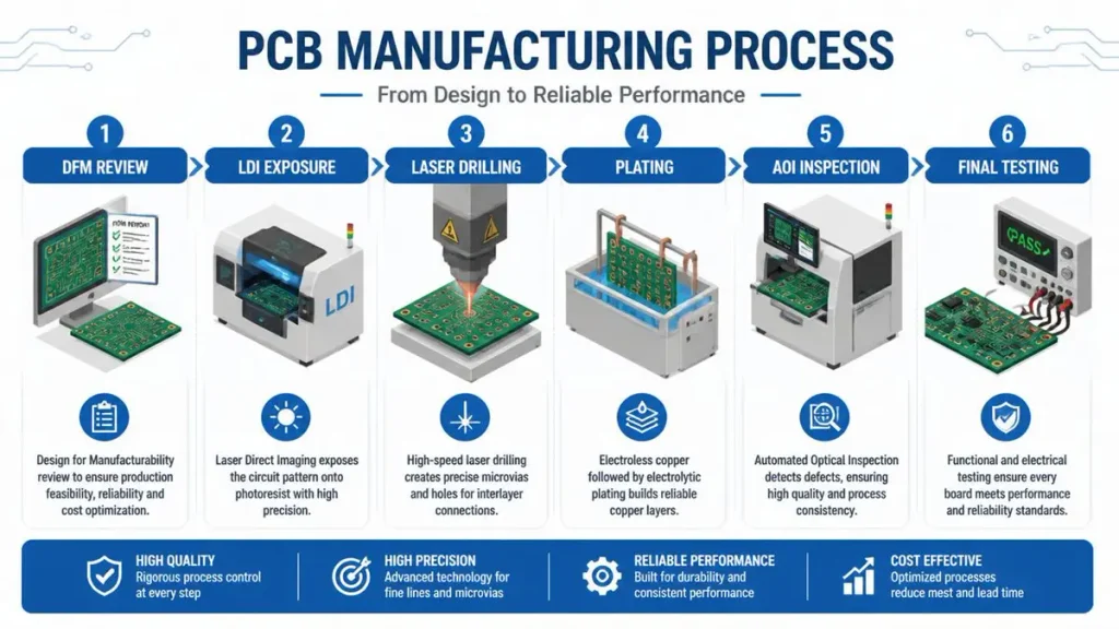
Custom PCB Manufacturing Process Flow
This is where advanced equipment decides whether a custom PCB manufacturer in China can actually build your board—or just quote it.
Engineering and DFM Review
Real engineers—not sales staff—check drill aspect ratios, copper balance, impedance feasibility, and annular ring against IPC-2221/2222 and IPC-6012.
CAM Data Preparation
Gerber/ODB++/IPC-2581 input, panelization, DRC, and tooling generation.
Material Preparation
Incoming laminate inspection (thickness, Dk, copper foil verification). Material substitution is the #1 quality risk in low-cost sourcing—we buy only from approved mills and keep mill certificates per lot.
Inner-Layer Imaging and Etching
LDI (Laser Direct Imaging) replaces film exposure in advanced plants, enabling ±2 μm registration—essential for mSAP and fine-line HDI, where stepper-based DI systems are becoming standard.
Lamination
Vacuum lamination with controlled press curves; sequential lamination for HDI.
Mechanical and Laser Drilling
Air-bearing CNC spindles at 150,000+ RPM for mechanical holes down to ~100 μm, plus UV and picosecond lasers for 50 μm microvias in thin build-up dielectrics.
Desmear and Copper Plating
Electroless + electrolytic copper; pulse plating with grain refiners to prevent dendrite formation at fine pitches.
Outer-Layer Imaging and Etching; Surface Finishing; Electrical Testing; Final Inspection
Standard outer-layer processing, final metallization, 100% E-test, IPC-A-600 final inspection, and packaging.
Custom PCB Manufacturing Process Flow: DFM → CAM → Materials → Inner-layer imaging/etch → Lamination → Drilling → Desmear/Plating → Outer-layer imaging/etch → Surface finish → E-test → Final inspection → Packaging.
What Advanced PCB Technologies Can a China Manufacturer Support?
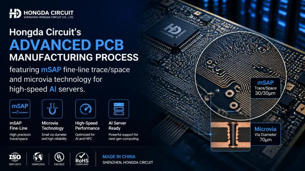
Advanced mSAP & Microvia PCB Technology by Hongda Circuit
This section separates a genuine factory from a “China PCB factory” brochure. As of 2026, mSAP has shifted from niche IC-substrate fabrication to the baseline for high-end fine-line production.
HDI and Microvia Technology
Stacked and staggered microvias, via-in-pad with filled plating, any-layer HDI.
mSAP and Fine-Line PCB Manufacturing
Modified semi-additive process: thin seed copper (1–3 μm), selective plating, flash etch. Subtractive etching becomes unreliable below ~25 μm line width due to undercut; mSAP achieves reliable features below 15 μm.
At Hongda Circuit: our mSAP line has been in continuous production since 2024, with 2026 capacity targeting 20/20 μm line/space in volume and 8/8 μm qualified for substrate-like PCB (SLP) builds. SLP technology is growing at roughly 11% CAGR through 2033, driven by AI accelerators and automotive electronics.
High-Layer PCB Manufacturing
20–40+ layer boards for backplanes and AI servers.
Controlled Impedance / Backdrilling / Heavy Copper / Embedded Components
Process-controlled impedance coupons, stub-reduction backdrilling for 112G SerDes, embedded resistor/capacitor layers.
High-Frequency and High-Speed PCB Manufacturing
RF laminate processing with plasma desmear; insertion-loss-controlled high-speed builds.
Why equipment matters for your keyword search: when you Google “custom PCB manufacturer China,” the factories that rank are often the ones with real mSAP/laser/LDI capability—because that’s what AI-era buyers now verify. Advanced equipment directly converts into ranking signals too: buyers share factory photos, equipment lists, and capability data, which generates the engagement Google measures.
How Does a Custom PCB Manufacturer Control Quality?
Incoming Material Inspection
Laminate certificates, foil thickness, Dk/Df verification.
Imaging Process Control
LDI calibration, registration monitoring.
AOI Inspection
Automated optical inspection after inner- and outer-layer etch.
X-Ray Inspection
Layer registration and microvia alignment verification.
Microsection Analysis
Per IPC-TM-650 methods—copper thickness, plating quality, dielectric thickness, annular ring.
Electrical Testing and Impedance Testing
100% E-test (flying probe or fixture), plus TDR impedance coupons on controlled-impedance lots.
Final Inspection and Manufacturing Traceability
IPC-A-600 final visual, lot/batch records retained for every shipment.
PCB Quality Control Checkpoint Table: IQC → Inner-layer AOI → Post-lamination X-ray → Plating microsection → Outer-layer AOI → E-test → Impedance test → FQC → Traceability archive.
Which PCB Standards and Certifications Should Buyers Check?
- IPC-6012 – qualification and performance of rigid PCBs (Class 1/2/3)
- IPC-6016 – HDI qualification
- IPC-A-600 – acceptability of PCBs
- IPC-TM-650 – test methods (microsection, thermal stress, etc.)
- ISO 9001 – quality management system
- IATF 16949 – automotive (required for automotive OEM supply chains)
- ISO 13485 – medical devices
- AS9100D – aerospace
- UL – flammability/safety listing (check the exact file and product scope)
- RoHS / REACH – environmental compliance
Critical principle: certification scope must match the product, facility, and your actual requirement. We advise buyers to verify certificate numbers against the certifier’s public database—this is a five-minute check that eliminates most trading-company fraud.
Can a China Custom PCB Manufacturer Support Prototype to Mass Production?
PCB Prototype → Engineering Validation → NPI → Pilot Production → Mass Production
The question every OEM should ask: can the same qualified process support the transition from prototype to volume? At Hongda Circuit, prototypes are built on the same lines, with the same materials and process recipes, as production lots—eliminating the classic re-qualification failure when a “prototype shop” hands off to a different mass-production factory. Production consistency is monitored via SPC on critical parameters (impedance, plating thickness, registration).
How Much Does Custom PCB Manufacturing in China Cost?
We deliberately do not publish a fixed price—any factory that quotes without your data is guessing.
What Factors Affect Custom PCB Cost?
| Cost Driver | Why It Changes Cost |
| Board size | Panel utilization |
| Layer count | Fabrication complexity |
| Material | Laminate cost (M8-class is several times standard FR-4) |
| Copper weight | Plating and etching |
| Trace/space | Process difficulty (mSAP commands a 50–100% premium over traditional HDI in today’s tight market) |
| Hole size / HDI | Drilling requirements, laser drilling, sequential lamination |
| Surface finish | Chemical/material cost (ENIG vs. OSP) |
| Testing | Inspection requirements |
| Quantity | Setup cost allocation |
| Lead time | Expedited manufacturing |
Why Is the Lowest PCB Quote Not Always the Lowest Total Cost?
Evaluate Total Cost of Ownership: unit price + engineering + tooling + testing + logistics + quality documentation + delivery risk + field-failure cost. In our experience, a board that fails in the field costs 50–100× its unit price by the time you count rework, shipping, and line-down time.
How Long Does Custom PCB Manufacturing in China Take?
Factory lead time ≠ total delivery time. Components: engineering review (1–2 days with complete data), fabrication (5–15 days typical, longer for sequential-lamination HDI/mSAP), inspection and testing (1–3 days), packaging, and international shipping (3–8 days express, 20–35 days sea freight). We quote per-order lead times based on actual line loading—never blanket promises.
What Risks Should Buyers Consider When Sourcing Custom PCBs From China?
Based on over a decade of factory audits and failure analyses we have performed for customers, the biggest pain points when manufacturing custom PCBs in China are:
- Material substitution – unapproved laminate swaps after qualification.
- Process changes – drill/etch parameters drifted to save cost.
- Quality consistency – prototype good, volume lots failing (the classic two-factory model).
- Communication and engineering support – sales teams answering engineering questions.
- Intellectual property protection – designs forwarded to third parties by brokers.
- Delivery risk – quoted lead times with no line-visibility.
- Prototype-to-production consistency – see above.
- Documentation and traceability – missing microsections, no lot records, unverifiable certificates.
The single most common root cause in our experience: the buyer never verified who actually owns the factory.
How Can You Verify a China PCB Supplier Is a Real Manufacturer?
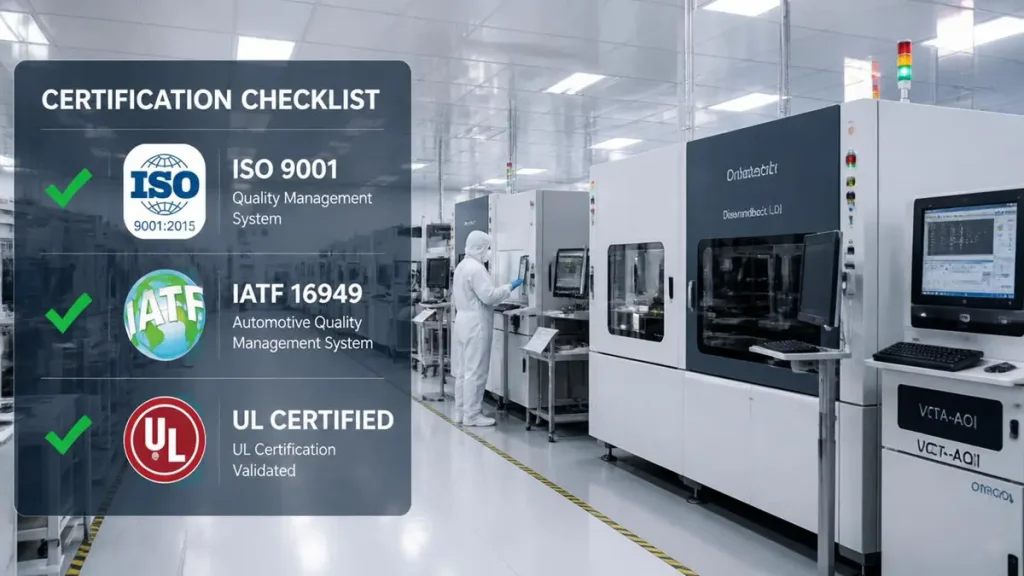
Custom PCB Manufacturer Certifications & Cleanroom Facility Verification
Factory vs Trading Company Verification Checklist:
- Verify the factory – business license scope, utility bills, photos with date, live video tour.
- Verify manufacturing equipment – ask for the laser drill count, LDI exposure systems, plating line type, AOI/X-ray machine models.
- Verify process capability – request capability matrix and recent microsection reports.
- Verify certifications – check certificate numbers in official databases.
- Request production samples – not marketing samples; boards from current production.
- Review inspection records – real factories produce them on demand.
- Conduct a factory audit – on-site or third-party (SGS, TÜV, BV).
- Evaluate engineering communication – ask a DFM question only a process engineer can answer.
How Should You Qualify a Custom PCB Manufacturer in China?
| Qualification | What Buyers Should Verify |
| Manufacturing | Actual process capability (L/S, microvia, layer count limits) |
| Materials | Approved material sources, mill certificates |
| Engineering | DFM capability, response time, stackup expertise |
| Quality | Inspection system (AOI, X-ray, microsection lab) |
| Testing | Electrical / reliability testing |
| Certification | Relevant certificates with correct scope |
| Capacity | Prototype to production on the same lines |
| Traceability | Batch / lot records |
| Delivery | Production planning visibility |
| Communication | Engineering-level response |
| Compliance | Customer / regulatory requirements (UL, IATF, RoHS) |
What Should You Include in a Custom PCB RFQ?
- PCB design files: Gerber, ODB++, or IPC-2581 + drill files.
- Technical specifications: layer count, dimensions, thickness, copper weight, material, trace/space, hole sizes, impedance, surface finish.
- Quality requirements: IPC class, testing, inspection, certification, reliability requirements (IST, thermal cycling).
- Commercial requirements: prototype quantity, production quantity, annual volume, target lead time, delivery destination.
How Should You Compare Quotes From China PCB Manufacturers?
Never compare unit price alone. Compare: PCB price + engineering + tooling + testing + logistics + quality documentation + delivery risk. If two quotes differ by more than ~20%, something material is different—material grade, testing coverage, or class level. Ask both factories to quote against an identical, itemized specification table.
Why Choose Hongda Circuit as Your Custom PCB Manufacturer in China?
Shenzhen Hongda Circuit Technology Co., Ltd. (www.pcbkr.com) is an engineering-led custom PCB manufacturer in Shenzhen, China, supporting OEMs worldwide.
Engineering-Led PCB Manufacturing
DFM review by process engineers, not sales scripts. Every RFQ receives a documented engineering assessment.
Prototype to Mass Production
Same lines, same materials, and the same qualified process—from your first custom PCB prototype to annual-volume production. For OEMs requiring low-volume production before scaling, see our small batch PCB manufacturing service.
Advanced PCB Manufacturing
HDI, any-layer interconnect, high-layer boards, heavy copper, rigid-flex—backed by our PCB manufacturing process.
mSAP, SLP, High-Speed and RF Capabilities
mSAP in continuous production since 2024; 20/20 μm line/space volume capability with 8/8 μm qualified for SLP builds; picosecond UV laser drilling for 50 μm microvias; Class 1000 cleanroom environment for SLP processing; advanced LDI with sub-micron alignment.
Quality Inspection and Testing
AOI, X-ray, in-house microsection lab (IPC-TM-650), 100% E-test, TDR impedance testing, full lot traceability. Our quality system is built around IPC-6012/6016 and ISO 9001, with automotive, medical, and aerospace programs supported per customer requirement.
Global OEM Support
English-speaking engineering interface, DDP/EXW logistics options, and supplier-qualification documentation packages (audit reports, certificates, capability matrices) for your vendor-management team.
Frequently Asked Questions About Custom PCB Manufacturing in China
What is a custom PCB manufacturer, and how is it different from a trading company?
A custom PCB manufacturer fabricates boards in its own factory with its own equipment and engineers; a trading company outsources your order, often without disclosure. Verify by equipment list, live video, microsection reports, and certificate scope.
How much does custom PCB manufacturing in China cost?
There is no fixed price. Cost is driven by board size, layer count, material, copper weight, trace/space, via structure, surface finish, testing, quantity, and lead time. Expect mSAP fine-line boards to cost 50–100% more than standard HDI. Request quotes against an identical spec sheet for meaningful comparison.
What is the MOQ for custom PCBs in China?
Hongda Circuit supports prototype quantities (as low as 1–5 pieces) through mass production. True factories can produce one-off prototypes economically because setup is digital (LDI/CAM); brokers often impose MOQs because they aggregate orders.
Can the same China PCB manufacturer handle HDI prototypes and mass production?
Yes—if the prototype is built on the same production lines with the same process recipe. At Hongda Circuit, prototype, NPI, and volume lots run through the same qualified process, preserving impedance, registration, and plating consistency across builds.
What certifications should I verify before placing an order?
At minimum: ISO 9001 and UL listing for general electronics; IATF 16949 for automotive; ISO 13485 for medical; AS9100 for aerospace. Verify the certificate number against the certifier’s public database—certificate scope, not the logo on a website, is what matters.
How do I protect my PCB design and IP when manufacturing in China?
Work directly with the factory (eliminating broker leakage), sign an NNN/IP agreement enforceable in China, control file distribution (ODB++/IPC-2581 rather than native CAD), and qualify suppliers on traceability and documentation discipline—not just price.
Request a Custom PCB Quote From a China Manufacturer
Request a Custom PCB Quote | Get a Free DFM Review | Discuss Your PCB Requirements With an Engineer
To receive an accurate quote, please provide: Gerber / ODB++ files, stackup, material, quantity, testing requirements, and target delivery date. Email: pcb@pcbkr.com
About Author
David Chen LinkedIn Profile
David Chen is a Senior RF/PCB Process Engineer at Shenzhen Hongda Circuit Technology Co., Ltd., with over 12 years of experience in high-frequency PCB fabrication, impedance-controlled stack-up design, and Rogers/PTFE laminate processing. He also boasts an extensive professional background in PCBA manufacturing, PCBA testing, and PCBA optimization, with specialized expertise in high-precision PCBA fault analysis and rigorous PCBA reliability testing. The author has worked with high-layer-count server PCB fabrication, ultra-low-loss backplane stackups, and thermo-mechanical reliability optimization for AI infrastructure projects involving 112G and 224G PAM4 architectures. Skilled in complex circuit design and cutting-edge advanced PCB manufacturing processes, he delivers solutions that elevate product durability and performance across industrial applications. His technical articles focusing on PCBA manufacturing workflows and testing methodologies are widely cited by industry peers and technical platforms, and have gained attention and recognition from industry colleagues.