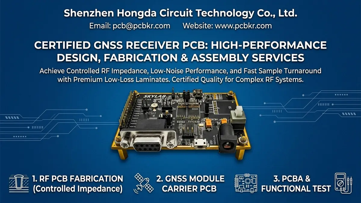
GNSS RECEIVER PCB Design, Manufacturing, and Assembly Guide
Building a dependable GNSS receiver PCB calls for tight RF impedance control, clean power delivery, thoughtful antenna integration, and consistent PCB production. Shenzhen Hongda Circuit Technology Co., Ltd. delivers RF PCB fabrication and PCBA services, helping OEMs turn GNSS designs into production‑ready hardware with clear inspection rules and performance validation criteria locked in upfront.
What Is a GNSS Receiver PCB and Why Does Manufacturing Quality Matter?
Simply put, a GNSS receiver PCB houses the RF signal path, antenna interface, receiver IC or module, power circuits and digital interfaces needed to pull in signals from satellite navigation constellations. Real‑world performance hinges on full electrical design plus physical board build — not just the receiver chip itself.
Global Navigation Satellite Systems, or GNSS, cover GPS, Galileo, BeiDou and GLONASS. Depending on receiver architecture, a board may support one or multiple constellations and frequency bands.
Before requesting pricing, OEM buyers need to tell these three product types apart:
- GNSS receiver PCB: Bare manufactured circuit board, no electronic components fitted.
- GNSS module carrier PCB: Base board for a pre‑soldered GNSS module, providing power, antenna and communication interfaces.
- GNSS receiver PCBA: Fully populated board with specified parts mounted; programming and functional testing may be included per agreement.
This distinction directly shapes material picks, assembly complexity, test scope and final quotations.
Which applications impose the most demanding GNSS PCB requirements?
| Application | Typical engineering challenge | Manufacturing priority |
|---|---|---|
| Drone flight controller | Switching regulator noise, ESC interference, compact antenna layout | RF isolation and power integrity |
| Automotive telematics | Wide temperature swings, vibration, co‑existence with cellular hardware | Material stability and repeatable assembly |
| Precision agriculture | Weak signal reception, multi‑band antenna operation | RF loss mitigation and antenna integration |
| Industrial IoT tracker | Tight enclosure constraints, low power draw, long service life | Compact layout and robust solder joints |
| Surveying and RTK receiver | Multi‑frequency reception, stable phase measurement | RF consistency and system‑level validation |
| Marine navigation | Moisture, corrosion, long continuous runtime | Surface finish quality, environmental resilience and reliability |
The key purchasing question is not whether a shop can make generic PCBs. It is whether they can build to your exact stackup, preserve critical RF geometries, fit your target components and run the tests your application demands.
What Are the Main Components of a GNSS Receiver PCB?
In short: a GNSS receiver PCB typically features an antenna interface, ESD protection, RF filter, LNA, receiver IC or module, reference clock, power management hardware and digital communication interfaces. The exact component chain follows your chosen receiver and antenna architecture.
A typical discrete RF front‑end signal flow works like this:
- GNSS antenna — captures satellite signals
- RF input and protection — connector, ESD safeguard and matching network as required
- RF filtering and LNA — signal filtering and amplification matched to system design
- GNSS receiver IC or module — processes signals and outputs navigation data
- Host processor and interfaces — UART, SPI, USB or other defined communication ports
This represents one common setup, not a mandatory sequence. Many receiver modules integrate onboard LNA, filtering and clock circuits. Active antennas carry their own amplifiers, while passive antennas need a different front‑end implementation.
Why does component placement affect receiver sensitivity?
The trace path running from antenna to receiver is often the layout’s most vulnerable section. Every connector, layer transition, filter and protection part adds parasitic effects or insertion loss.
Small‑looking placement trade‑offs in dense layouts can shift real‑world RF behaviour. Moving a filter further from the receiver input lengthens sensitive signal traces. Routing switching regulator traces underneath the RF input creates unwanted crosstalk. Adding protection hardware without checking its parasitic capacitance can throw off impedance matching at operating frequencies.
Good engineering workflow follows this order: lock down RF architecture, follow receiver and antenna reference design guidance, finalise stackup, then complete layout review before sending files to manufacturing.
How Should You Design a GNSS Receiver PCB for Low‑Noise RF Performance?
A solid GNSS receiver PCB design starts with the antenna and RF signal chain. It uses properly calculated transmission lines, maintains uninterrupted return‑current paths, keeps noisy circuits separate from sensitive RF nodes, and validates assembled hardware under real‑world operating conditions.
How should GNSS RF traces and impedance be controlled?
50 Ω single‑ended RF interfaces are standard for GNSS hardware, though your exact impedance target should come from component and interface datasheets.
For controlled‑impedance builds, your manufacturer needs these details:
- Finalised PCB stackup and dielectric thickness values
- Dielectric material specifications including frequency‑dependent properties
- Copper thickness, accounting for finished conductor profiles post‑processing
- Transmission‑line topology: microstrip or grounded coplanar waveguide
- Target impedance value plus acceptable tolerance range
- Placement of impedance test coupons and agreed measurement methodology
Trace width cannot be set in isolation from stackup parameters. A 50 Ω trace built on thin dielectric will have very different physical dimensions compared with one on thicker core material.
Shenzhen Hongda Circuit Technology Co., Ltd. offers RF PCB capabilities including high‑frequency material options, electromagnetic simulation and controlled‑impedance production. Their public high‑frequency service documentation lists 50 Ω single‑ended impedance targets with ±3 % or ±2 Ω tolerance. Confirm exact specs and test coverage for every individual GNSS project.
How should the ground plane and return path be designed?
Where your RF topology requires it, keep the reference plane fully intact underneath RF transmission lines. Split planes, poorly managed connector transitions or gaps under traces distort electromagnetic fields and introduce impedance discontinuities.
- Never run RF feed traces across ground‑plane splits
- Add ground stitching vias around RF transitions where appropriate
- Adhere strictly to antenna vendor ground‑plane and keep‑out zone requirements
- Keep switching nodes and fast digital traces well clear of RF input zones
- Audit return‑current routing around connectors, filters and layer change points
- Limit unnecessary vias along high‑sensitivity RF routes
Via stitching alone cannot fix poor layout decisions. Via placement, ground continuity and transmission‑line geometry must work in tandem.
How should the antenna matching network be handled?
Design your matching network around your actual antenna, enclosure, ground plane and operating bands — do not simply copy reference board schematics from unrelated projects.
Practical workflow: source or measure your antenna’s impedance characteristics, stick to vendor layout recommendations, and add tuning footprints if on‑board adjustment will be needed.
An antenna performing well on an evaluation kit can shift behaviour once fitted inside metal enclosures or placed near batteries, displays, cellular antennas or wiring looms. Always validate matching performance in your final mechanical assembly.
How Do PCB Materials and Stackup Choices Affect GNSS Receiver Performance?
PCB material selection and stackup geometry directly shape RF insertion loss, impedance repeatability, dimensional stability and antenna‑feed performance. FR‑4 works well for many compact GNSS applications. Low‑loss laminates make sense for longer RF traces, higher‑frequency bands or systems with tight RF performance budgets.
Should you choose FR‑4 or a low‑loss RF laminate?
| Design condition | Material‑selection approach | Main consideration |
|---|---|---|
| Compact design using integrated GNSS module | Start evaluation with FR‑4 | Cost, producibility, short RF trace lengths |
| External antenna paired with short feed line | Compare FR‑4 loss against system loss budget | Connector and trace‑transition losses |
| Multi‑band GNSS with strict RF layout constraints | Justify RF‑grade laminate use through performance review | Frequency‑dependent Dk, Df and stackup structure |
| Long RF feed path or tightly regulated RF system | Run loss and impedance analysis | Cumulative signal attenuation and discontinuities |
| Dense board combining multiple RF and digital interfaces | Evaluate stackup alongside return‑path design | Crosstalk, isolation and routing limits |
Dielectric constant (Dk) defines transmission‑line geometry and electrical trace length. Dissipation factor (Df) drives dielectric signal loss. Copper roughness, final copper thickness and conductor profile also raise insertion loss, an effect that grows at higher frequencies.
Shenzhen Hongda Circuit Technology Co., Ltd. supports high‑frequency PCB production with Rogers, Taconic and other RF‑grade laminates alongside specialised high‑volume fabrication workflows. These material options serve suitable GNSS projects, but always select laminate grade against your operating frequency, loss budget and material supply availability.
Does every GNSS receiver PCB need HDI technology?
No. HDI delivers value when component pitch, board footprint, routing density or interconnection requirements call for laser‑drilled microvias and sequential lamination. Standard two‑layer or four‑layer stacks often offer better cost efficiency and simpler manufacturing when electrical and mechanical targets are satisfied.
HDI helps pack receiver modules, memory, power management and multiple communication interfaces onto small form‑factor boards. It will not inherently improve GNSS sensitivity or positioning accuracy.
Hongda Circuit’s HDI services cover laser‑drilled microvias and sequential lamination constructions. For GNSS work, deploy HDI only for genuine miniaturisation or routing bottlenecks — not just because finer production processes are available.
How should the stackup be approved before production?
Your signed‑off stackup must list every copper layer, dielectric material, dielectric thickness, copper weight and all controlled‑impedance requirements. For multi‑layer boards, engineering review also needs to cover layer registration, lamination behaviour and RF reference‑plane positioning.
One key manufacturing nuance: finished conductor geometry deviates from original CAD data due to etching compensation and plating processes. Your manufacturer must tune production parameters to hit target finished impedance, rather than treating Gerber trace width as final electrical geometry.
Before releasing a GNSS PCB to production, buyer and manufacturer need mutual agreement on stackup revision, impedance targets, test‑coupon strategy and deliverable documentation for the order.
How Can Advanced PCB Manufacturing Equipment Improve GNSS Receiver PCB Quality?
Modern imaging tools, laser drilling, precision lamination, impedance engineering and automated inspection help preserve fine RF geometries, maintain layer alignment, cut down manufacturing defects and boost batch‑to‑batch consistency. Real‑world benefit depends on your board’s actual design rules and process controls applied to each production run.
For Shenzhen Hongda Circuit Technology Co., Ltd., meaningful manufacturing capability is not defined by the smallest feature sizes their equipment can theoretically produce. What counts is reliably translating your defined RF design into repeatable finished hardware, documenting key process parameters and verifying requirements that matter to your product.
Which advanced processes are most relevant to GNSS PCB manufacturing?
1. Laser Direct Imaging (LDI)
LDI creates circuit patterns via digitally controlled exposure. With proper process calibration, it delivers sharper fine‑line definition and tighter layer‑to‑layer registration.
Hongda Circuit’s public PCB capability documentation references AI‑enhanced LDI control and 15/15 µm line/space capacity for high‑density work. Note this represents maximum process capability; most GNSS boards do not require 15/15 µm feature sizes.
2. Laser drilling and HDI interconnection
Laser drilling forms microvias for dense multi‑layer layouts. It lets designers route compact components without relying exclusively on large mechanical vias.
Hongda Circuit’s via‑fill and HDI resources detail UV and CO₂ laser‑drilling workflows plus copper‑filled microvia capacity. These features apply to GNSS projects needing compact routing, fine‑pitch parts or multi‑layer module carrier boards.
3. Precision lamination and dimensional control
Lamination quality governs dielectric thickness, layer registration and overall board geometry. These factors carry weight for RF designs relying on precise spacing between signal traces and their reference planes.
For multi‑layer GNSS PCBs, manufacturing reviews must validate agreed material build‑up, lamination sequence and finished thickness targets. Top‑of‑the‑range pressing hardware alone cannot guarantee RF performance without controlled raw materials and inspection steps.
4. Controlled‑impedance engineering and TDR
Time‑domain reflectometry (TDR) characterises impedance across transmission paths or dedicated test coupons. Useful results hinge on good coupon design, instrument calibration, test methodology and pre‑agreed pass‑fail thresholds.
Hongda Circuit’s RF PCB service covers TDR‑based impedance verification and electromagnetic simulation. Buyers should confirm exactly which measurements, coupons and reports get included within their quotation.
5. Automated optical inspection and electrical testing
AOI catches visible pattern defects such as shorts, opens, scratches and residual copper. Electrical testing validates continuity and isolation per your test specification.
Neither test proves real‑world GNSS sensitivity or positioning accuracy. RF system performance requires separate validation if written into product acceptance criteria.
Why does manufacturing precision matter even when GNSS signals are relatively low‑frequency?
Satellite signals reaching GNSS antennas arrive extremely weak. Extra signal loss and unintended interference degrade performance even when your board does not demand the ultra‑fine routing used for high‑speed server hardware.
Take a compact receiver with 50 Ω RF input, LNA and filter. If manufactured trace geometry diverges from design assumptions, or connector launch points create impedance discontinuities, reflection rises. Poor ground return paths worsen RF transitions. Final assembled hardware can underperform against simulation or reference‑board results.
That said, not every dimensional shift causes measurable receiver issues. Outcomes vary with operating frequency, electrical trace length, discontinuity magnitude, antenna setup and receiver noise budget. Good engineering practice identifies high‑sensitivity features first and applies manufacturing controls proportional to their real‑world impact.
For this reason, controlled processes tied to clear specifications deliver far more value than isolated marketing claims about minimum trace widths.
What Are the Most Common GNSS Receiver PCB Manufacturing Problems?
Key production‑related risks include impedance drift, inconsistent RF connector launch performance, dielectric thickness variation, unreliable solder joints, unapproved component swaps, surface contamination and insufficient isolation between noisy circuits and the RF front‑end. Solid production planning flags these risks pre‑fabrication and assigns appropriate inspection or validation steps for each one.
The scenarios below reflect established RF and PCB manufacturing engineering best practices. They serve as practical failure‑analysis examples and do not refer to specific past incidents at Hongda Circuit.
Why can a GNSS receiver work on the prototype but fail after mass production?
Prototypes often use hand‑picked components, carefully assembled antennas and ideal lab test environments. Mass‑volume manufacturing introduces component‑lot spread, assembly variability, supply‑chain shifts and differences from final enclosure or cabling configurations.
| Manufacturing symptom | Likely cause to investigate | Recommended verification |
|---|---|---|
| RF performance varies between production batches | Stackup deviation, finished geometry shift or raw‑material inconsistency | Cross‑check stackup documentation and impedance test records |
| Reception performance shifts post‑reflow soldering | Component damage, soldering faults or altered RF matching | Carry out assembly inspection plus pre‑ and post‑reflow measurement comparison |
| Only some units exhibit weak reception | Component tolerance spread, connector soldering quality or inconsistent antenna contact | Side‑by‑side testing of known‑good and failing units |
| Performance drops once hardware sits inside its enclosure | Antenna detuning, cable routing effects or enclosure‑induced coupling | Repeat testing in full final mechanical configuration |
| Failure triggers when nearby radios transmit | GNSS desensitisation from adjacent transmitters or power‑supply coupling | Compare receiver behaviour with transmitter switched on versus off |
During debugging, avoid modifying multiple variables simultaneously. If you adjust antenna, matching components, power supply and enclosure all at once, isolating the root fix becomes very difficult.
What happens when impedance is correct on paper but wrong on the finished PCB?
One frequent engineering pitfall: approving CAD‑defined trace width without reviewing the actual production stackup. Real‑world impedance depends on finished conductor profile and dielectric structure: copper thickness, etch profile, dielectric spacing and bulk‑material properties all play a role.
Follow this more robust workflow:
- Request manufacturer‑proposed production stackup
- Recalculate controlled‑impedance geometries for that exact build‑up
- Lock in finished impedance target plus tolerance limits
- Agree test‑coupon layout and measurement procedure
- Archive measurement results tied to each production lot
When specifying a 50 Ω RF interface, always define acceptable tolerance before manufacturing commences. A nominal impedance value on its own does not set acceptance rules.
How should RF connector and soldering defects be investigated?
An RF connector can feel mechanically secure yet deliver poor electrical transition performance. Root causes may include bad launch geometry, solder bridging, ground‑pin flaws, pad damage or footprint‑to‑stackup mismatch.
AOI spots visible soldering defects, but connectors that look fine under visual inspection can still contain RF discontinuities. Depending on interfaces and available lab equipment, troubleshooting may call for continuity checks, microscopy, TDR or network‑analyser characterisation.
For fine‑pitch receiver modules, X‑ray inspection reveals hidden solder joints where applicable. Always match inspection methodology to package construction and suspected failure mode.
How can component substitutions damage GNSS performance?
Replacement LNAs, filters, protection diodes or matching‑network parts may drop straight onto your footprint yet carry different electrical characteristics.
Before signing off on alternate components, engineering teams must compare application‑critical parameters: operating frequency, gain, noise figure, input‑output matching, insertion loss, linearity, parasitic capacitance, supply requirements and package parasitics.
Enforce formal approved‑alternate‑parts workflows. Procurement should never authorise electrically unvalidated swaps purely to work around long component lead times.
How Should GNSS Receiver PCB Assemblies Be Tested Before Shipment?
Split testing into four distinct categories: bare‑board electrical integrity, assembly workmanship, interface functionality and GNSS radio reception performance. Your required test suite follows product specifications; no single inspection covers all four dimensions.
Which tests should buyers include in the acceptance plan?
| Test category | What it verifies | Important limitation |
|---|---|---|
| Bare‑board electrical test | Defined connectivity and isolation | Does not validate RF reception capability |
| Impedance testing | Characteristic impedance on coupons or target structures | Coupon measurements may not represent every real‑world RF transition |
| AOI | Visible assembly and soldering defects | Cannot inspect all hidden solder joints |
| X‑ray inspection | Select hidden solder joints and internal construction | Does not prove end‑to‑end RF performance |
| Power and interface test | Supply behaviour plus UART, USB, SPI and other interfaces | Does not validate satellite signal acquisition |
| GNSS functional test | Reception and navigation behaviour under defined conditions | Results vary with antenna hardware, test setup and signal environment |
| Environmental validation | Performance across target temperature, vibration and other stress conditions | Must align with formal product qualification plans |
Which GNSS performance metrics should be defined?
For products requiring GNSS functional validation, specify these practical metrics:
- Time to First Fix (TTFF): Duration needed to achieve valid position lock under documented starting conditions
- Carrier‑to‑noise density ratio (C/N₀): Standard metric for comparing received satellite signal strength against noise floor
- Acquisition and tracking performance: Ability to lock onto and maintain target satellite signals
- Positioning repeatability: Measurement consistency under controlled test conditions
- Multi‑constellation / multi‑band operation: Confirm support for constellations and frequency bands your product requires
Write acceptance criteria specific to your receiver hardware, antenna, firmware and test setup. For example, never directly compare cold‑start TTFF figures against warm‑start results without acknowledging differing initial system states.
PCB suppliers need clear scope boundaries for their testing services. Bare‑board fabrication inspection, PCBA visual checks, receiver‑module verification and full system‑level GNSS validation represent separate service deliverables.
What evidence should accompany a production shipment?
- Approved PCB stackup and raw‑material traceability records
- Bare‑board electrical‑test reports
- Impedance‑test data, if required by design specifications
- Assembly inspection logs plus agreed X‑ray output
- Component traceability and approved‑alternate documentation
- Functional‑test results matching pre‑agreed acceptance criteria
- Non‑conformance records and corrective‑action reports where applicable
Not every project needs the full set of documents. Your purchasing specification should list mandatory deliverables and clarify whether testing runs 100 % per‑unit, via sampling or only on first‑article samples.
How Do You Choose a GNSS Receiver PCB Manufacturer in China?
Select your manufacturer based on RF engineering support, controlled‑impedance processes, stackup and material capability, assembly workmanship, inspection scope, traceability and capacity to hit your volume and timeline targets. General‑purpose PCB production capacity alone does not prove competence for GNSS‑focused builds.
What should OEM procurement teams verify before placing an order?
- RF engineering capability: Confirm whether the supplier can review your proposed stackup, impedance rules, RF trace geometry, connector launch layouts and antenna‑related layout constraints. Clarify whether they offer only fabrication DFM review or deeper RF‑oriented engineering input.
- Material and process capability: Confirm exact laminate grades, copper build‑up, finished thickness, surface finish and layer structures are available for your order. A vendor’s broad material list does not guarantee availability for your specific stackup or lead‑time window.
- Inspection and test capability: Ask for their planned impedance verification workflow, bare‑board test coverage, AOI / X‑ray scope and available functional‑test services. Finalise acceptance criteria before issuing purchase orders.
- Component sourcing and traceability: For PCBA orders, understand how they manage manufacturer part numbers, approved alternates, component provenance, moisture‑sensitive device handling and formal change approvals.
- Production scaling: Confirm support for prototypes, engineering revisions, pilot builds and repeat volume orders without losing revision control. Clarify tooling, test‑fixture ownership and production‑record retention.
- Communication and delivery: Request itemised quotations separating PCB fabrication, component procurement, assembly, testing, non‑recurring engineering and logistics. Understand what triggers production start and which factors could cause delays.
Why consider Shenzhen Hongda Circuit Technology Co., Ltd. for GNSS PCB manufacturing?
Shenzhen Hongda Circuit Technology Co., Ltd. provides PCB fabrication and PCBA assembly, with documented capacity for high‑frequency materials, controlled‑impedance production, HDI structures and associated assembly workflows. These capabilities serve GNSS projects needing compact hardware, managed RF routing or unified PCB‑plus‑assembly supply chains.
Match your process selection to real‑board requirements for any GNSS project:
- Standard multi‑layer fabrication for boards where routing density and electrical requirements do not demand HDI
- Controlled‑impedance production when RF interfaces and transmission‑line geometry require tight tolerances
- High‑frequency laminate options where system loss budgets justify the extra cost
- HDI and laser microvia workflows only when packaging or routing density creates hard constraints
- PCBA assembly plus defined inspection packages when you order fully populated receiver hardware
Advanced equipment expands manufacturing options, but it cannot replace design reviews, first‑article validation and well‑defined acceptance criteria. The best production solution is always the simplest process that reliably meets product specifications.
For procurement teams, the logical next step is to submit board data and test requirements for engineering review — rather than selecting manufacturing processes purely based on minimum feature‑size figures.
How Much Does GNSS Receiver PCB Manufacturing Cost and What Affects Lead Time?
GNSS receiver PCB cost depends on board dimensions, layer count, laminate grade, impedance requirements, drilling and fabrication complexity, component sourcing, assembly volume and test scope. Lead time is driven by raw‑material stock levels, production scheduling, engineering approval cycles and component procurement timelines.
Which factors have the greatest impact on quotation accuracy?
| Cost driver | Why it matters | Information needed for quotation |
|---|---|---|
| PCB stackup | Layer count, material grade and dielectric build‑up set base fabrication cost | Finalised layer stack and material specification |
| Controlled impedance | Requires engineering review, special geometry and agreed verification steps | Target impedance plus tolerance window |
| HDI structure | Microvias and sequential lamination add extra production stages | Via topology and fabrication notes |
| Surface finish | Must suit component soldering and long‑term reliability requirements | ENIG or other specified finish type |
| Component sourcing | Part availability, product lifecycle status and approved alternates shape cost and lead time | Full BOM with original manufacturer part numbers |
| Assembly complexity | Fine‑pitch packages, shielding and special handling increase process difficulty | Assembly drawings and component package details |
| Functional testing | Custom test fixtures and GNSS validation add engineering and test labour | Test‑plan documentation and acceptance thresholds |
| Order quantity | Non‑recurring setup costs amortise differently across prototype versus volume batches | Prototype quantities plus production‑volume forecast |
Practical quotations should separate non‑recurring engineering and fixture charges from per‑unit recurring pricing. Clearly state whether pricing covers bare‑PCB build, component procurement, PCBA assembly, functional testing and freight.
How can buyers reduce cost without sacrificing GNSS performance?
- Use conventional multi‑layer stackups whenever routing and RF targets are satisfied
- Specify low‑loss laminates only when operating frequency and loss budget genuinely justify them
- Avoid overly aggressive line‑space rules if standard manufacturing geometry meets requirements
- Consolidate component sourcing and formally approve alternate parts through engineering review
- Define streamlined repeatable test plans instead of paying for open‑ended or duplicated testing
- Review Gerber files, stackup documents, BOM and assembly drawings before releasing production orders
Never cut costs by omitting essential ground planes, swapping RF components without validation or loosening impedance rules without formal engineering assessment.
How Can You Request a GNSS Receiver PCB Manufacturing Quote from Hongda Circuit?
Submit your PCB fabrication files, stackup definition, impedance requirements, BOM, assembly data, order quantity and test specifications. Shenzhen Hongda Circuit Technology Co., Ltd. will assess your manufacturing scope and flag technical or sourcing issues needing resolution prior to production launch.
What information should you include in an RFQ?
- Gerber or ODB++ output plus drill data
- Approved stackup and laminate specifications
- RF impedance targets and tolerance limits
- PCB dimensions, finished thickness, copper weight and surface‑finish requirements
- BOM including manufacturer part numbers and pre‑approved alternate parts
- Pick‑and‑place files and assembly drawings
- Prototype and production order volumes
- Required inspection scope and GNSS functional‑test rules
- Target delivery date plus shipping destination
For full turn‑key PCBA projects, also clarify who supplies GNSS modules, antennas, RF components, firmware, programming fixtures and end‑of‑line test hardware. Resolving responsibilities early eliminates gaps in quotation coverage.
Request a GNSS Receiver PCB quotation Email: pcb@pcbkr.com
Send your PCB files and project targets to the engineering team to discuss fabrication, assembly and suitable validation workflows.
5 FAQs for Buyers Searching for a GNSS PCB Supplier on Google
How do I choose a reliable GNSS receiver PCB manufacturer?
Evaluate their controlled‑impedance expertise, RF‑focused engineering support, material traceability, fabrication quality, PCBA inspection capability and ability to execute tests matching your design requirements. Ask for tangible documented proof of project‑relevant capabilities instead of relying purely on generic marketing statements.
Can Shenzhen Hongda Circuit manufacture and assemble a complete GNSS receiver PCB?
Shenzhen Hongda Circuit Technology Co., Ltd. delivers PCB fabrication and PCBA assembly services. Feasibility for a full GNSS receiver assembly depends on board design, BOM completeness, component availability, assembly constraints and agreed functional‑test scope.
What files are required to get a GNSS receiver PCB quotation?
For bare‑PCB quoting: Gerber or ODB++ datasets, drill files, stackup definition, material and thickness specs, impedance requirements, copper weight and surface‑finish details. For PCBA, add BOM, pick‑and‑place data, assembly drawings, order quantities and test requirements.
How can a PCB manufacturer help reduce GNSS receiver signal loss and interference?
Manufacturing teams implement your approved stackup and transmission‑line geometry, hold fabrication tolerances in check, run DFM reviews and verify impedance targets. That said, overall receiver sensitivity also comes from antenna design, RF component selection, power integrity, enclosure effects and full‑system interference testing.
What should I compare when evaluating GNSS PCB manufacturing quotes?
Make direct comparisons against identical stackup, laminate grade, finished copper weight, impedance tolerance, via construction, surface finish, component‑sourcing terms, assembly scope, test coverage, lead time and quality deliverables. Lower unit pricing offers no advantage if critical testing, component traceability or needed engineering work gets excluded.
About Author
David Chen LinkedIn Profile
David Chen is a Senior RF/PCB Process Engineer at Shenzhen Hongda Circuit Technology Co., Ltd., with over 12 years of experience in high-frequency PCB fabrication, impedance-controlled stack-up design, and Rogers/PTFE laminate processing. He also boasts an extensive professional background in PCBA manufacturing, PCBA testing, and PCBA optimization, with specialized expertise in high-precision PCBA fault analysis and rigorous PCBA reliability testing. The author has worked with high-layer-count server PCB fabrication, ultra-low-loss backplane stackups, and thermo-mechanical reliability optimization for AI infrastructure projects involving 112G and 224G PAM4 architectures. Skilled in complex circuit design and cutting-edge advanced PCB manufacturing processes, he delivers solutions that elevate product durability and performance across industrial applications. His technical articles focusing on PCBA manufacturing workflows and testing methodologies are widely cited by industry peers and technical platforms, and have gained attention and recognition from industry colleagues.