Telemetry Module PCB: Design, Manufacturing, and Assembly for Reliable Remote Monitoring
A telemetry module PCB connects sensors, processing circuits, power management, and wired or wireless communication interfaces to collect and transmit remote data. Reliable telemetry hardware depends on appropriate PCB stackup, RF layout, noise control, low-power design, component selection, and manufacturing quality. For OEM buyers, selecting a capable PCB and PCBA manufacturer is essential for repeatable performance from prototype validation to volume production.
Table of Contents
- What Is a Telemetry Module PCB and How Does It Work?
- Which Applications Require a Custom Telemetry Module PCB?
- How Should Engineers Choose a PCB Stackup for a Telemetry Module?
- How Do RF Layout and Antenna Design Affect Telemetry PCB Performance?
- How Can a Telemetry Module PCB Reduce Power Consumption?
- How Should Engineers Control EMI, Noise, and Signal Integrity?
- Which PCB Materials and Surface Finishes Are Suitable for Telemetry Modules?
- What Manufacturing Processes Are Important for Telemetry Module PCBs?
- What Are the Most Common Telemetry Module PCB Manufacturing Defects?
- How Should Buyers Compare Telemetry Module PCB Manufacturers?
- What Files Should Buyers Submit for a Telemetry PCB Manufacturing Quote?
- How Can Buyers Reduce Telemetry PCB Costs Without Sacrificing Reliability?
- How Should a Telemetry Module PCB Move From Prototype to Mass Production?
- Why Choose Shenzhen Hongda Circuit Technology Co., Ltd.?
- Frequently Asked Questions
What Is a Telemetry Module PCB and How Does It Work?
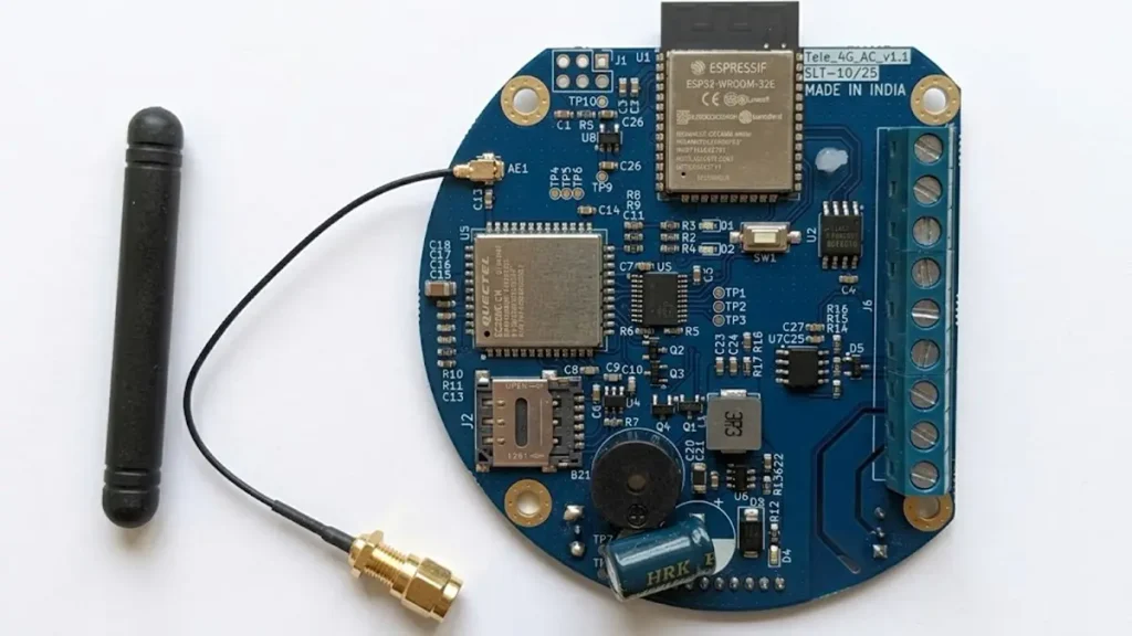
A telemetry module PCB integrates wireless communication, sensor interfaces, and power management for reliable remote data acquisition.
A telemetry module PCB is a printed circuit board designed to collect, process, and transmit measurements or operating data from remote equipment. It integrates electronic components that enable communication between sensors, a controller, and a receiving system.
A typical telemetry module contains several functional blocks:
- Sensor interface: Receives analog or digital signals from temperature, pressure, vibration, position, current, or other sensors.
- Signal conditioning: Filters noise, adjusts signal levels, and prepares sensor signals for processing.
- Data processing: Uses a microcontroller, processor, or dedicated logic to acquire and process measurements.
- Communication interface: Transmits data through technologies such as UART, RS-485, CAN, LoRa, Wi-Fi, Bluetooth, or cellular networks, depending on the application.
- Power management: Regulates input power and supplies appropriate voltages to the controller, sensors, and communication circuitry.
- Protection circuitry: Provides appropriate protection against electrostatic discharge, electrical transients, reverse polarity, or other identified risks.
The exact architecture depends on the application. A battery-powered environmental sensor may prioritize sleep current and compact dimensions, while an industrial telemetry gateway may require multiple interfaces, stronger electrical protection, and continuous operation.
What Is the Difference Between Telemetry PCB, Telemetry PCBA, and a Complete Telemetry Module?
These terms describe different stages of product development and manufacturing.
| Term | Scope | Typical deliverable |
|---|---|---|
| Telemetry PCB | Bare printed circuit board | Fabricated circuit board without components |
| Telemetry PCBA | Printed circuit board with electronic components assembled | Assembled electronic board |
| Complete telemetry module | Electronic hardware integrated with required firmware, enclosure, antenna, and other system elements as specified | Application-ready module or subsystem |
For procurement teams, this distinction is important when requesting quotations. A bare PCB quotation does not necessarily include component sourcing, SMT assembly, programming, functional testing, enclosure integration, or wireless performance validation.
At Shenzhen Hongda Circuit Technology Co., Ltd., buyers can discuss their required PCB fabrication and PCBA assembly scope through PCBKR.
Which Applications Require a Custom Telemetry Module PCB?
Custom telemetry PCBs are suitable for products that require specific sensor interfaces, communication technologies, power limits, mechanical dimensions, environmental protection, or system integration.
| Application | Key Engineering Considerations | Manufacturing Priorities |
|---|---|---|
| Industrial equipment monitoring | Sensor accuracy, electrical noise, communication reliability | Process consistency, soldering quality, and interface testing |
| Remote sensor nodes | Low power consumption, compact dimensions, analog signal integrity | Appropriate assembly precision and control of leakage current |
| LoRa and LPWAN devices | Antenna matching, RF layout, long battery life | Consistent board geometry and assembly quality |
| Cellular telemetry gateways | RF coexistence, transient power demand, multiple interfaces | Multilayer routing, power integrity, and functional validation |
| Energy monitoring systems | Measurement accuracy, voltage and current sensing, electrical protection | Appropriate insulation design and assembly quality |
| Vehicle and mobile equipment monitoring | Vibration, temperature, transient supply conditions | Connector reliability and mechanical robustness |
| Environmental monitoring equipment | Humidity, weak signals, long-term stability | Suitable materials, protective coatings where appropriate, and environmental validation |
| Remote infrastructure monitoring | Long operating periods, communication availability, maintainability | Traceability, revision control, and repeatable testing |
Standard development boards may be sufficient for early proof-of-concept work. Commercial products, however, often require a custom PCB layout to satisfy enclosure constraints, production cost targets, connector requirements, and environmental specifications.
Defining system requirements before selecting the PCB construction helps reduce redesign risk and allows the manufacturer to identify fabrication constraints early.
How Should Engineers Choose a PCB Stackup for a Telemetry Module?
The appropriate PCB stackup depends on routing density, RF frequency, grounding, signal integrity, power distribution, mechanical dimensions, and production cost. There is no universally optimal layer count for every telemetry module.
Should You Choose a Two-Layer, Four-Layer, or Six-Layer PCB?
| PCB Construction | Potential Advantages | Important Considerations |
|---|---|---|
| Two-layer PCB | Lower manufacturing complexity and cost for simpler layouts | Limited routing flexibility and more challenging ground-plane management in dense designs |
| Four-layer PCB | Additional routing capacity and dedicated ground or power planes | Higher fabrication cost than a comparable simple two-layer board |
| Six-layer PCB | Greater routing flexibility for complex interfaces and compact layouts | More stackup planning, lamination requirements, and cost |
| HDI PCB | Supports dense routing, fine-pitch components, and compact designs | Requires suitable microvia structures, tighter process controls, and greater manufacturing complexity |
A four-layer PCB may be a practical starting point for a compact telemetry design containing a microcontroller, RF transceiver, analog sensor circuits, and several external interfaces. This is a design option, not a universal requirement; simpler products may work well with two layers.
Which Stackup Parameters Should Buyers Specify? Specify?
Procurement documents should identify the following requirements where applicable:
- Number of copper layers.
- Finished board thickness and permitted tolerance.
- Copper weight for internal and external layers.
- Minimum track width and spacing.
- Minimum finished hole diameter.
- Dielectric material and relevant electrical properties.
- Controlled-impedance nets and target impedance.
- Board dimensions, edge clearances, and connector positions.
- Surface finish and solder-mask requirements.
- Electrical testing and acceptance criteria.
For RF or high-speed interfaces, the stackup must be evaluated as a complete structure. Trace width alone does not determine impedance; dielectric thickness, material properties, copper geometry, and reference-plane configuration also matter.
A qualified manufacturing review should identify potential mismatches between the design files and the selected production process before fabrication begins.
How Do RF Layout and Antenna Design Affect Telemetry PCB Performance?
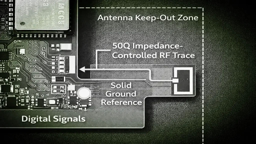
RF layout, controlled-impedance routing, grounding, and antenna integration help maintain telemetry signal integrity and wireless communication performance
RF performance depends on the entire signal path, including the transceiver, matching network, transmission line, ground reference, antenna, enclosure, and surrounding components. A correctly fabricated PCB cannot compensate for every antenna or system-integration problem.
What Should Engineers Check in a Wireless Telemetry PCB?
Antenna placement and clearance: Follow the antenna manufacturer’s layout guidance. Keep prohibited copper, components, cables, and enclosure structures out of designated antenna clearance areas.
Controlled impedance: Many RF interfaces use a 50-ohm system, but the required impedance must be confirmed from the selected radio, antenna, and transmission-line design. The actual target and tolerance should be documented in the fabrication package.
Ground reference: Preserve the intended RF return path. Unplanned splits or interruptions in a reference plane can increase discontinuities and degrade signal performance.
Matching network: Provide the components and layout required by the RF design. Leave tuning provisions when justified by the design and validation plan.
Digital and power noise: Avoid placing noisy switching circuits or high-speed digital routing where they interfere with sensitive RF or analog sections.
Enclosure integration: Plastic housings, metal brackets, cables, batteries, and nearby structures can change antenna behavior. Validate the assembled product rather than relying exclusively on bare-board measurements.
Which RF Tests Should Be Included in the Procurement Specification?
Depending on the product, testing may include:
- RF impedance or transmission-line verification where applicable.
- Antenna return loss or S11 measurement.
- Voltage standing wave ratio (VSWR) measurement where relevant.
- Transmitter output power and receiver sensitivity testing.
- Frequency accuracy and spectral measurements.
- Wireless communication testing in the intended enclosure.
- Applicable regulatory and radio-equipment compliance testing.
Not every PCB manufacturer performs every system-level RF test. Buyers should distinguish bare-board fabrication testing, PCBA electrical testing, RF subsystem validation, and final product certification when defining supplier responsibilities.
How Can a Telemetry Module PCB Reduce Power Consumption?
A telemetry module’s energy consumption is determined primarily by component selection, circuit architecture, firmware behavior, operating conditions, and communication activity. PCB layout and manufacturing quality can influence power losses, leakage, noise, and stability, but a low-power claim must be verified at the system level.
Which Power Parameters Should Buyers Evaluate?
| Parameter | Why it matters | Recommended verification |
|---|---|---|
| Standby current | Determines energy consumption during idle periods | Measure current after the specified sleep state is reached |
| Active current | Represents normal sensing and processing activity | Measure under a defined workload |
| Transmit peak current | Can cause supply droop or resets | Capture current and supply voltage during transmission |
| Power-supply efficiency | Affects battery life and heat generation | Measure input and output power across representative loads |
| Leakage current | Can be significant in very low-power designs | Measure under specified voltage, temperature, and board conditions |
| Wake-up behavior | Affects energy consumption and response time | Verify sleep-to-active transitions and operating sequence |
How Does PCB Layout Affect Power Reliability?
Short, appropriately sized power paths can reduce unwanted voltage drop. Proper placement of decoupling capacitors supports transient current demand. Suitable grounding and separation of sensitive analog circuits from noisy switching circuitry can also reduce measurement errors.
For battery-powered designs, the engineer should evaluate the complete duty cycle, including sensing, processing, transmitting, receiving, and sleep periods. A board that draws little current while idle may still consume substantial energy if the radio transmits frequently or repeatedly reconnects to a network.
Buyers should request measured power data with the supply voltage, firmware version, test mode, temperature, and measurement method documented.
How Should Engineers Control EMI, Noise, and Signal Integrity?
Electromagnetic interference (EMI), conducted noise, and poor signal integrity can reduce measurement accuracy, interrupt communication, or cause intermittent system resets. Effective mitigation combines circuit design, PCB layout, component selection, protection, and validation testing.
Which Design Practices Matter Most?
Separate noisy and sensitive circuitry. Keep switching power stages and high-current paths away from sensitive analog inputs where practical.
Maintain continuous reference planes. Plan signal return paths before routing critical traces. Avoid forcing signals across unintended plane splits.
Protect external interfaces. Select ESD, surge, and transient protection based on the interface, cable length, operating environment, and applicable standards.
Control differential signals. For CAN, USB, and other differential interfaces, follow the transceiver and interface specifications for routing, termination, and topology.
Validate power integrity. Test the supply rail during radio transmission, sensor acquisition, startup, and other high-demand operating conditions.
Test the assembled product. Cable routing, connectors, enclosure materials, grounding, and firmware can affect EMC behavior. PCB-level inspection alone cannot establish full system compliance.
Which Interfaces May Be Used on a Telemetry PCB?
| Interface | Common use | Key design consideration |
|---|---|---|
| UART | Module configuration and serial data exchange | Logic levels, baud rate, grounding |
| RS-485 | Industrial serial communication | Termination, topology, transient protection |
| CAN | Distributed control and monitoring | Bus termination, transceiver selection, protection |
| I²C | Short-distance communication between on-board components | Pull-up sizing, capacitance, bus speed |
| SPI | High-speed communication between local components | Trace routing, signal integrity, clock behavior |
| Ethernet | Networked monitoring and gateways | Interface requirements, isolation where applicable, routing |
| RF interfaces | Wireless data transmission | Impedance, antenna integration, RF layout |
The selected interface should match the application rather than being added simply because it is common in other designs.
Which PCB Materials and Surface Finishes Are Suitable for Telemetry Modules?
Material selection should follow the electrical requirements, operating frequency, temperature range, environmental conditions, assembly process, and budget. FR-4 is suitable for many telemetry applications, while low-loss laminates may be justified for demanding RF designs.
FR-4 or a Low-Loss RF Laminate?
FR-4 is widely used because of its availability, manufacturing familiarity, and cost effectiveness. For many low- and moderate-frequency telemetry circuits, it may provide adequate electrical performance.
Higher-performance RF laminates may be appropriate when transmission-line loss, dielectric stability, or other electrical constraints exceed what the selected FR-4 construction can satisfy. The decision should be based on the operating frequency, route length, loss budget, stackup, and validated material data.
Buyers should avoid specifying expensive RF materials without an engineering reason. They should also avoid substituting a material without approval when the original design depends on its electrical properties.
How Should Buyers Select a Surface Finish?
| Surface finish | Potential benefits | Important considerations |
|---|---|---|
| ENIG | Flat solderable surface and suitability for many fine-pitch assemblies | Cost, process control, storage, and application requirements |
| Lead-free HASL | Often economical and widely used | Surface flatness may be unsuitable for some fine-pitch packages |
| OSP | Flat surface and suitability for certain assembly processes | Handling, storage, and assembly-process constraints |
| Immersion silver | Flat surface suitable for selected applications | Tarnishing, handling, and storage considerations |
The final choice should be compatible with the component package, assembly process, required contact performance, and expected storage conditions.
For products exposed to humidity, condensation, dust, or corrosive environments, consider conformal coating or other protective measures where appropriate. Coating does not replace sound layout, material selection, enclosure design, and environmental testing.
What Manufacturing Processes Are Important for Telemetry Module PCBs?
Reliable telemetry hardware requires a manufacturing process that matches the board’s design complexity and documented acceptance criteria. Important operations may include material preparation, imaging, etching, lamination, drilling, copper plating, solder-mask application, surface finishing, electrical testing, component assembly, and final inspection.
Which PCB Fabrication Controls Affect Reliability?
Imaging and etching: Track width and spacing must remain within the agreed fabrication limits. Fine-line requirements should be reviewed against the actual copper thickness and production process.
Multilayer lamination: Layer registration, dielectric thickness, material compatibility, and lamination control affect the finished board structure.
Drilling and plating: Hole size, registration, plating quality, and the applicable acceptance requirements influence electrical connectivity and via reliability.
Solder mask and surface finish: Mask registration, solderable surfaces, and finish quality affect assembly and the protection of copper features.
Electrical testing: Bare-board continuity and isolation testing can identify specified opens and shorts, but they do not verify the functionality of an assembled telemetry module.
Why Does PCBA Assembly Require Separate Controls?
Surface-mount technology (SMT) and through-hole technology (THT) address different component and connection requirements. A telemetry module may combine fine-pitch controllers, RF components, sensors, and mechanically robust connectors.
Assembly controls may include solder-paste printing, component placement, reflow profiling, polarity checks, through-hole soldering, and inspection. The required process depends on the component packages and board design.
For products containing fine-pitch components or hidden solder joints, AOI and X-ray may provide complementary inspection coverage. Neither method detects every possible defect, and inspection should be combined with suitable electrical or functional testing.
Which Manufacturing Capabilities Should Be Verified Before Ordering?
| Capability | What buyers should confirm |
|---|---|
| Multilayer PCB fabrication | Supported layer count, material systems, thickness, and tolerances |
| Fine-line fabrication | Minimum line width and spacing for the specified copper construction |
| Controlled impedance | Supported structures, design inputs, tolerance, and verification method |
| SMT and THT assembly | Package range, assembly process, and inspection coverage |
| AOI and X-ray | Applicable defects, package coverage, and inspection criteria |
| Electrical testing | Bare-board or assembled-board scope and test limitations |
| Functional testing | Required fixtures, firmware, test procedures, and acceptance criteria |
| Revision control | Management of approved fabrication files, BOMs, and assembly instructions |
Shenzhen Hongda Circuit Technology Co., Ltd. can review telemetry PCB fabrication and PCBA assembly requirements against the project’s documented specifications. Exact capability limits and testing arrangements should be confirmed during quotation and engineering review.
What Are the Most Common Telemetry Module PCB Manufacturing Defects?
Common risks include open or short circuits, soldering defects, poor component alignment, damaged pads, via defects, incorrect components, and intermittent connector connections. However, communication failures and inaccurate sensor readings can also result from circuit design, firmware, antenna integration, or system-level problems.
| Observed problem | Possible causes | Recommended investigation |
|---|---|---|
| Intermittent wireless connection | Antenna detuning, RF layout issues, supply instability, firmware or network problems | RF measurements, power-rail capture, communication logs |
| Incorrect sensor readings | Analog noise, calibration error, grounding, sensor interface or solder defects | Reference measurements, calibration checks, circuit inspection |
| Unexpected resets | Supply droop, transient current, poor connections, firmware faults | Oscilloscope measurements, load tests, reset logs |
| Communication failure | Incorrect wiring, solder defects, interface configuration, termination or firmware issues | Continuity checks, interface testing, protocol analysis |
| Excessive standby current | Incorrect operating state, component leakage, contamination, design problems | Current measurement, power-domain isolation, visual inspection |
| Failure after environmental exposure | Corrosion, moisture ingress, material incompatibility, insufficient protection | Environmental testing, microscopy, failure analysis |
How Can Buyers Reduce Repeat Defects?
Start with an engineering review before fabrication. Confirm the approved stackup, footprints, connector positions, polarity, test points, BOM revision, and manufacturing notes.
During prototype production, use the results to identify design weaknesses and assembly risks. Before mass production, freeze the approved design revision and define inspection criteria, functional test coverage, traceability requirements, and procedures for handling nonconforming products.
A structured failure-analysis process should identify the actual cause rather than automatically attributing every field failure to fabrication.
How Should Buyers Compare Telemetry Module PCB Manufacturers?
Buyers should evaluate manufacturers using documented process capability, engineering support, component sourcing, quality controls, testing, traceability, production planning, and total delivered cost.
A supplier that can fabricate a basic PCB may not necessarily be equipped to deliver the complete assembled and tested telemetry module. Confirm the required scope before comparing quotations.
What Should Be Included in a Supplier Evaluation?
| Evaluation criterion | Questions to ask |
|---|---|
| Fabrication capability | Can the supplier meet the specified layer count, dimensions, materials, and tolerances? |
| RF and impedance support | Can the required stackup and impedance structures be manufactured and verified as agreed? |
| Assembly capability | Can the supplier assemble the selected packages, connectors, and mixed-technology components? |
| Component sourcing | Are manufacturer part numbers, traceability, and substitution approval managed appropriately? |
| Quality control | Which defects are covered by AOI, X-ray, electrical inspection, and functional testing? |
| Engineering support | Is DFM feedback available before fabrication and assembly? |
| Revision control | How are Gerber files, BOMs, assembly data, and test programs controlled? |
| Production scalability | How will prototype results be translated into a repeatable production process? |
| Commercial terms | What are the quotation scope, lead-time assumptions, payment terms, and shipping conditions? |
| Communication | Can technical questions and corrective actions be handled clearly and promptly? |
Why Should Buyers Consider a Manufacturer That Supports Both PCB and PCBA?
Coordinating fabrication and assembly through a single manufacturing partner can reduce handoff complexity. It may also simplify responsibility for DFM feedback, production scheduling, revision management, and defect investigation.
However, an integrated service is valuable only when the supplier’s actual capabilities and quality processes meet the project requirements. Buyers should establish which operations are performed in-house, which are subcontracted, and who is responsible for final acceptance.
What Files Should Buyers Submit for a Telemetry PCB Manufacturing Quote?
A complete request for quotation (RFQ) should define the bare-board requirements, assembly scope, component specifications, quantities, inspection criteria, and delivery expectations. Complete documentation helps suppliers provide comparable quotations and identify engineering risks before production.
Telemetry PCB Fabrication Checklist
Provide the following files and requirements where applicable:
- Gerber or ODB++ fabrication data.
- NC drill files and finished board outline.
- Layer stackup and material requirements.
- Board thickness and copper weight.
- Controlled-impedance requirements and target values.
- Surface finish and solder-mask specifications.
- Panelization or array requirements, if applicable.
- Electrical test and acceptance requirements.
Telemetry PCBA Assembly Checklist
For assembled boards, also provide:
- BOM with manufacturer part numbers and approved alternatives.
- Pick-and-place or centroid file.
- Assembly drawings and component polarity notes.
- Component datasheets or special handling instructions where necessary.
- Required programming, calibration, or firmware-loading procedures.
- Functional test procedures and acceptance limits.
- Packaging, labeling, and traceability requirements.
Which Commercial Details Should Be Included?
Specify prototype quantity, pilot quantity, estimated annual demand, target delivery date, destination, and whether the order includes customer-supplied or turnkey components.
Also identify any regulatory, environmental, reliability, or product-specific acceptance requirements. If files are preliminary, label the revision clearly and indicate what remains subject to engineering approval.
Request a Telemetry PCB and PCBA Quote: Visit PCBKR or email pcb@pcbkr.com with your fabrication files, BOM, required quantities, and testing scope.
How Can Buyers Reduce Telemetry PCB Costs Without Sacrificing Reliability?
The best cost reductions usually come from simplifying the design where technically appropriate, improving panel utilization, selecting suitable materials, controlling component sourcing, and avoiding preventable prototype rework.
Which Cost Drivers Should Procurement Teams Review?
Layer count and stackup: Use the simplest construction that satisfies routing, grounding, and signal-integrity requirements.
Material selection: Avoid specifying expensive low-loss materials unless the electrical requirements justify them.
Board dimensions and panelization: Review outline geometry, spacing, tooling requirements, and production-panel utilization with the manufacturer.
Copper and fabrication requirements: Specify fine lines, unusual thicknesses, and tight tolerances only where necessary.
Component availability: Identify obsolete, long-lead-time, or single-source components before production planning.
Assembly complexity: Review component placement, package selection, connector installation, and test accessibility during DFM.
Testing strategy: Identify the tests necessary to control product risk. Remove redundant activities only when engineering evidence supports the change.
Prototype learning: Correct design problems before committing to larger production quantities.
Should Buyers Select the Lowest PCB Quotation?
Not necessarily. A low initial price may exclude component sourcing, programming, fixtures, functional testing, special inspection, packaging, or shipping.
Compare quotations on the same technical and commercial basis. A useful comparison includes the bare PCB price, assembly cost, component cost, tooling or test-fixture charges, inspection scope, logistics, expected rework exposure, and delivery commitments.
The objective is to minimize total delivered cost while maintaining the required performance and quality level.
How Should a Telemetry Module PCB Move From Prototype to Mass Production?
A controlled production ramp progresses from design review and prototype fabrication to assembly validation, pilot production, acceptance testing, and a documented production release.
Step 1: Complete Engineering and DFM Review
Review fabrication files, stackup, component footprints, BOM availability, assembly clearances, RF requirements, and test-point accessibility.
Resolve manufacturing questions before releasing the production files.
Step 2: Build and Validate Prototypes
Evaluate the assembled board against the intended operating requirements. Depending on the product, validation may include power consumption, sensor accuracy, interface operation, RF performance, temperature behavior, and electrical protection.
Record design issues and corrective actions so that the next revision can be assessed consistently.
Step 3: Conduct Pilot Production
Build a representative quantity using the intended manufacturing and assembly processes. Review assembly yield, inspection results, functional test coverage, component traceability, and process repeatability.
Pilot acceptance criteria should be agreed before the build.
Step 4: Release the Approved Production Revision
Freeze the approved fabrication data, BOM, assembly drawings, firmware version, test procedures, and acceptance criteria.
Establish a change-control process for component substitutions, stackup changes, process changes, and design revisions.
Step 5: Monitor Production Quality
Review inspection results, functional test failures, nonconformances, corrective actions, and supplier changes. For products with ongoing demand, establish appropriate traceability and periodic quality reviews.
A successful prototype is an important milestone, but it does not by itself demonstrate production consistency. Repeatable manufacturing depends on controlled processes, documented requirements, and evidence from representative builds.
Why Choose Shenzhen Hongda Circuit Technology Co., Ltd. for Telemetry Module PCB Manufacturing?
Shenzhen Hongda Circuit Technology Co., Ltd. supports OEM procurement discussions for PCB fabrication and PCBA assembly through its PCBKR website. The right manufacturing arrangement depends on the required board construction, components, testing, production quantities, and delivery expectations.
For a telemetry module project, buyers should establish the following during the engineering review:
- PCB fabrication requirements: Layer count, material, copper weight, finished thickness, minimum features, and impedance needs.
- PCBA assembly requirements: SMT, THT, component packages, sourcing arrangements, and assembly documentation.
- Quality verification: Appropriate inspection, electrical testing, functional testing, and agreed acceptance criteria.
- Production planning: Prototype and production quantities, component availability, revision control, and delivery schedule.
- Technical coordination: DFM questions, engineering clarifications, approved substitutions, and nonconformance handling.
For RF-intensive or low-power products, provide the intended operating frequency, antenna configuration, power budget, and key system-level performance requirements early. These details help the manufacturing team distinguish fabrication constraints from issues that require circuit redesign or system validation.
When reviewing a supplier, buyers should also confirm applicable certifications, equipment capability, actual test coverage, and any outsourced operations rather than relying on general marketing claims.
Request a Custom Telemetry Module PCB Quote
Whether you are developing an industrial remote-monitoring device, a wireless sensor node, a telemetry gateway, or a connected control system, early manufacturing review can help identify fabrication and assembly risks before production.
Contact Shenzhen Hongda Circuit Technology Co., Ltd.
- Website: https://www.pcbkr.com/
- Email: pcb@pcbkr.com
To receive a useful quotation, include your Gerber or ODB++ files, stackup requirements, BOM, assembly drawings, required quantities, and testing specifications.
Request your telemetry PCB fabrication or PCBA assembly quote today.
Frequently Asked Questions About Telemetry Module PCB
What is a telemetry module PCB?
A telemetry module PCB is a circuit board that connects sensing, processing, power management, and communication functions to collect and transmit remote data. Its construction depends on the application, interfaces, power budget, operating environment, and required communication performance.
What is the difference between a telemetry PCB and an IoT PCB?
A telemetry PCB focuses on acquiring and transmitting measurements or operating data. An IoT PCB may also support cloud connectivity, automation, user interfaces, and edge processing. The categories overlap, so the appropriate design depends on the system requirements rather than the product label.
Which PCB layer count is best for a telemetry module?
There is no universally optimal layer count. Two-layer boards can suit simpler designs, while four- or six-layer boards may provide more routing flexibility and improved reference-plane planning. The final choice should follow routing density, grounding, RF requirements, dimensions, and cost.
Does a telemetry module PCB require controlled impedance?
Not every telemetry PCB requires controlled impedance on every signal. RF transmission lines and some high-speed interfaces commonly require defined impedance. Buyers should confirm the target, tolerance, relevant stackup, and verification method with the design team and manufacturer.
Which materials are suitable for wireless telemetry PCBs?
FR-4 can meet the requirements of many telemetry designs. Low-loss laminates may be appropriate when frequency, route length, and the signal-loss budget justify them. Material selection should be based on validated electrical properties, fabrication compatibility, and total cost.
How do you test a telemetry module PCBA?
Testing may include visual inspection, AOI, X-ray for suitable packages, electrical checks, programming verification, interface testing, and functional testing. RF and environmental validation may also be required. The final plan should match the product’s failure risks and agreed acceptance criteria.
Can a telemetry PCB manufacturer provide turnkey PCBA?
A turnkey supplier can coordinate bare PCB fabrication, component sourcing, assembly, and agreed testing. Buyers should confirm which services are included, how substitutions are approved, how components are traced, and who is responsible for programming and functional validation.
What files are required for a telemetry PCB quote?
Typical requirements include Gerber or ODB++ data, drill files, stackup information, board dimensions, and fabrication notes. Assembly quotations also require a BOM, pick-and-place data, assembly drawings, quantities, and testing requirements. Complete documentation helps reduce quotation delays and scope misunderstandings.
How can buyers reduce telemetry PCB manufacturing costs?
Buyers can review layer count, materials, panelization, component sourcing, assembly complexity, and avoidable rework. DFM review before prototyping can identify manufacturing risks early. Cost reductions should not compromise required electrical performance, environmental protection, or agreed acceptance criteria.
What should buyers compare when choosing a telemetry PCB manufacturer in China?
Compare verified fabrication capabilities, PCBA assembly, engineering support, component sourcing, inspection and testing, traceability, production planning, communication, and total delivered cost. Ask suppliers to confirm specific requirements and provide appropriate evidence before placing an order.
About Author
David Chen LinkedIn Profile
David Chen is a Senior RF/PCB Process Engineer at Shenzhen Hongda Circuit Technology Co., Ltd., with over 12 years of experience in high-frequency PCB fabrication, impedance-controlled stack-up design, and Rogers/PTFE laminate processing. He also boasts an extensive professional background in PCBA manufacturing, PCBA testing, and PCBA optimization, with specialized expertise in high-precision PCBA fault analysis and rigorous PCBA reliability testing. The author has worked with high-layer-count server PCB fabrication, ultra-low-loss backplane stackups, and thermo-mechanical reliability optimization for AI infrastructure projects involving 112G and 224G PAM4 architectures. Skilled in complex circuit design and cutting-edge advanced PCB manufacturing processes, he delivers solutions that elevate product durability and performance across industrial applications. His technical articles focusing on PCBA manufacturing workflows and testing methodologies are widely cited by industry peers and technical platforms, and have gained attention and recognition from industry colleagues.